Commercialization of Gallium Nitride Nanorod Arrays on Silicon
for Solid-State Lighting
MASSACH US, Fby
SEP 12 2008
Qixun Wee
_...,P•
QES
B.Eng. Chemical and Biological Engineering, Division of Bioengineering Nanyang Technological University, 2007
SUBMITTED TO THE DEPARTMENT OF MATERIALS SCIENCE AND ENGINEERING
IN PARTIAL FULFILLMENT OF THE REQUIREMENTS FOR THE DEGREE OF
MASTER OF ENGINEERING IN MATERIALS SCIENCE AND ENGINEERING AT THE
MASSACHUSETTS INSTITUTE OF TECHNOLOGY SEPTEMBER 2008
© 2008 Massachusetts Institute of Technology All rights reserved "I"
Signature of Author: ...
Department of Materials Science and Engineering August 5, 2008 Certified by: ... Stavros S; Certified by: ... ... Carl V. Thompson II alapatas Professor of Materials Science and Engineering
Thesis Supervisor
Soo-Jin Chua Professor of Electrical and Computer Engineering, National University of Singapore Thesis Co-supervisor
Accepted by: ... ....
Samuel M. Allen POSCO Professor of Physical Metallurgy Chair, Departmental Committee on Graduate Students
ARCHNEs
Commercialization of Gallium Nitride Nanorod Arrays on Silicon
for Solid-State Lighting
by
Qixun Wee
Submitted to the Department of Materials Science and Engineering on August 5, 2008 in Partial Fulfillment of the
Requirements for the Degree of Master of Engineering in Materials Science and Engineering
ABSTRACT
One important component in energy usage is lighting, which is currently dominated by incandescent and fluorescent lamps. However, due to potentially higher efficiencies and thus higher energy savings, solid-state lighting (SSL) is seriously being considered as a replacement. Currently, state-of-the-art white LEDs are made up of thin films of GaN and InGaN grown on sapphire substrates. A new LED structure design is proposed, in which GaN nanorod arrays are grown on silicon substrates. This new structure could be fabricated using anodized aluminum oxide's (AAO) ordered arrangement of pores as a template for growth of the nanorod array.
AAO is selected for its high porosity and simple controllability of pore size and separation,
which can in turn produce high density monocrystalline nanorod arrays with adjustable rod size and separation. Several advantages are enjoyed by LEDs based on rod arrays: lower cost, better yield and reliability and higher efficiencies. Two more LED designs, other than the current state-of-the-art GaN LED and the proposed LED structure, are included for comparisons. It is found that the proposed LED structure design is the best after considering costs and efficiency. For commercialization of this new LED design, the market penetration plan is to have a partnership with one of the major players in the current white LED industry. This has the advantage of having minimal capital investment and the product could be sold under an established brand. A simplified projection of earnings is calculated to illustrate sustainability of this business plan.
Thesis Supervisor: Carl V. Thompson II
Acknowledgements
This thesis will probably be impossible without the help of several individuals. First, I would like to thank Professor Carl V. Thompson II, my thesis supervisor. He has been exceptionally helpful in guiding me to complete this thesis. Although he has many other commitments himself, I am grateful that he is always happy to have discussion sessions with me. Prof. Thompson has also offered me his research students' help in my thesis. I am very fortunate that they are also very accommodating towards me. Hence, I would like to thank some of Prof. Thompson's students, Jihun Oh and Steve Boles, for providing insights to this thesis.
I would like to extend my gratitude toward Professor Chua Soo-Jin, my thesis co-supervisor,
who guided my work while I am in Singapore. He is always obliging towards me and provided me with useful references. In fact, many ideas in this thesis are derived from his contributions. In addition, I want to thank my fellow peers in the SMA, who make my graduate life vibrant and memorable. I also want to specially thank Boon Hooi, for delivering my draft thesis to the DMSE office. Finally, I would like to thank my family for their support and care during my academic pursuit.
Table of Contents
ABSTRACT... 2
Acknow ledgem ents ... 3
List of Figures ... ... 6
List of Tables... ... 7
1. Introduction and M otivation ... ... 8
1.1. M otivation to solid-state lighting application ... 8
1.1.1. Potential savings in energy... ... 8
1.1.2. Huge m arket ... ... 8
1.2. M otivation to using GaN ... ... 9
1.2.1. Direct band gap ... ... 9
1.2.2. Large band gap and associated alloy's w ide range of energies ... 9
1.2.3. Standard w hite LED m aterial ... 10
1.3. M otivation to using nanorods ... ... 10
1.3.1. Quantum confinem ent ... 10
1.3.2. High quality crystal ... . 11
1.3.3. Geom etrical advantage in light extraction ... 12
1.4. M otivation for using silicon substrates ... . 12
1.5. Com m ercial viability ... 13
2. Com peting Technologies ... 14
2.1. State-of-the-art w hite LEDs... ... 14
2.2. Organic light em itting diodes ... ... 15
2.3. Incumbent lighting technologies: fluorescent & incandescent lamps... 16
3. Proposed Device ... ... 18
4. Nanofabrication of Nanorods ... ... 19
4.1. Tem plate synthesis... ... 19
4.1.1. Form ation of AAO m em brane ... ... 19
4.1.2. Deposition to form GaN nanorods ... ... 21
4.2. Catalyst-assisted vapor-liquid-solid ... ... 21
5. Proposed Fabrication Procedures ... ... 24
6. Com parative Advantages ... ... 25
6.1. Low er costs... ... 25
6.2. Yield & reliability ... ... 26
6.3. Higher efficiencies ... ... 26
6.4. Overall com parison ... ... 28
7. Patent Research... ... 29
7.1. US 7,132,677: invented by Hwa-Mok Kim, Tae-Won Kang & Kwan-Soo Chung ... 29
7.2. US 7,294,862: invented by Jonathan J Wierer, Michael R Krames & Mihail M Sigalas...30
7.3. US 2007/0158639: invented by Chien-Cheng Yang, Zhi-Cheng Hsiao & Gen-Wen Hsieh ... 30
8. Business M odel ... ... 31 8.1. M arket size ... ... 31 8.2. Supply chain ... ... 31 8.3. Business plan... ... 32 8.4. Returns projections ... ... 33 8.5. Funding sources ... ... 35 9. Conclusion...36 References... ... 37
List of Figures
Figure 1 - A plot of solar spectrum flux (left) compared with a plot of band gap energy of Inl-xGaxN alloy (right). The researchers in Lawrence Berkeley National Laboratory (LBNL) showed in 2002 that InN has a
band gap of 0.7 eV instead of the previously reported value of 2.0 eV. Diagram from reference [6]... 9
Figure 2 - Sketch of the novel LED structure ... ... ... 10
Figure 3 - Stages of nanorod growth to remove threading dislocation. Adapted from reference [1]...11
Figure 4 - Schematic of how threading dislocations do not affect the defect density of a nanorod beyond a certain aspect ratio. Adapted from reference [17] ... 12
Figure 5 - Possible LED structures. (a) GaN film on a sapphire substrate. (b) GaN film on a silicon substrate. (c) GaN nanorod array on a sapphire substrate. (d) GaN nanorod array on a silicon substrate. ...1 3 Figure 6 -Schematic structure of the state-of-the-art GaN-InGaN LED on a sapphire substrate. Derived from reference [20] ... 14
Figure 7 - Schem atic diagram of an OLED. ... 15
Figure 8 - Proposed design of an LED structure. (a) Top view of GaN nanorod array. (b) Schematic cross-sectional view of proposed LED structure ... 18
Figure 9 - SEM images of AAO surfaces. Right: the AAO is anodized after pretexturing with a SiC mold by mechanical molding. Left: the AAO is untextured. Image adapted from reference [36] ... 20
Figure 10 - SEM images of long-range ordered arrays of pores in AAO arranged in a square lattice, possible through pre-patterning. Adapted from reference [39]. ... ... 21
Figure 11 - Schematic of the catalytic VLS process for growth of nanorods. Adapted from reference [45]. ...22..
Figure 12 - SEM of GaN nanorods grown by nanocapillary condensation. (a) GaN nanorods protrude out of the nanotrenches. (b) Cross-sectional view of a GaN nanorod. (c) Top-view of a GaN nanorod. From reference [30]...23
Figure 13 - Fabrication steps. ... ... 24
Figure 14 - Design of Patent 7,132,677. ... ... 29
Figure 15 - Design of Patent 7,294,862. ... ... 30
Figure 16 - Design of Patent 2007/0158639. ... 30
Figure 17 - Supply chain of existing LED industry. Boxed area represents the participation of most dom inant LED com panies in the supply chain. ... 31
List of Tables
Table 1 - Typical performance and cost of incandescent, fluorescent and white LED lamps. Note that the
white LED has much lower efficacy than laboratory prototypes. Figures from references [3] and [27]... 16
Table 2 - Consolidated ranking order of the four LED designs from Figure 5, with 1 being the best ... 28
Table 3- Total lamps in US in 2001. Retrieved from reference [3] ... .... 31
Table 4 - Profit projections over 5 years of manufacturing, taking 1% of Osram sales ... 34
1. Introduction and Motivation
So far, fossil fuels remain our main energy sources. Although renewable energy sources are available, they are insufficient to replace non-renewable energy sources yet. Hence, it is the interest of the general public to be energy efficient, so as to prolong the lifetime of fossil fuels and perhaps buy more time for renewable energy sources to develop and become sufficient for world consumption. One important component in energy usage is lighting. Currently, general illumination is dominated by both incandescent lamps and fluorescent lamps. However, due to
potentially higher efficiency and thus higher energy savings, solid-state lighting (SSL) is seriously being considered as a replacement to these incumbent lighting technologies.
SSL is a generalized term for light emitting diodes (LEDs) that produce light for illumination purposes. The Department of Energy (DOE) in the United States (US) realized the potential benefits that SSL could provide in replacing incumbent lighting technologies, and created a national strategy to promote the transition to SSL into the market.
1.1. Motivation to solid-state lighting application
There exist many applications for gallium nitride (GaN) nanorod arrays. They could be use to make white LEDs, diode lasers, solar cells or photodetectors. Among these useful applications, the white LED is selected as the choice for applications, because it is the least complex (a pn junction) among the listed applications. This implies a shorter development time. Its application
could also be implemented in a wide variety of markets such as display illumination, signboard lighting and general lighting.
1.1.1. Potential savings in energy
The Optoelectronics Industry Development Association (OIDA) has estimated that SSL could potentially reduce global usage of electricity for lighting by 50% [2]. This not only means savings in terms of the cost of energy, it also translates into massive reduction of carbon emission. The US Department of Energy (DOE) also recognized this potential savings in energy, and they created a technology roadmap for SSL development [3].
1.1.2. Huge market
General lighting is a huge market. It is estimated that approximately 10 to 15% of the total electricity usage is for lighting purposes [4]. Illumination using LEDs (or solid-state lighting) is an emerging market that is still growing rapidly. The US federal government also supports using solid-state lighting for general illumination, because of its lower electrical power consumption. The DOE also greatly supports research and development in solid-state lighting. All this makes it favorable to be in the solid-state lighting industry.
1.2. Motivation to using GaN
GaN is a Ill-V compound semiconductor made up of two elements, group III gallium and group V nitrogen. GaN has several properties that are ideal for making optoelectronic devices [5]. It has direct band gap, a large band gap, high thermal conductivity and chemical stability.
1.2.1. Direct band gap
GaN and many of its associated compounds have direct band gaps. This means that when carriers recombine, they combine directly with no loss of momentum. The energy of the recombination, which is equal to the band gap energy, will be emitted in the form of a photon. This is called radiative recombination, which is the basis of how LEDs work. In the case of indirect band gaps, direct recombination is impossible without phonons. Recombination is also possible through mediation of a defect, for example, which is inefficient. Hence, having direct band gap is a prerequisite for building efficient LEDs.
1.2.2. Large band gap and associated alloy's wide range of energies
4 3 1 -Q 4 31
5 4 3 2 1 0.0 0.2 0.4 0.6 0.8 1.0Solar Flux Ga content in
(10~ phttonsseml2Ipm)
In,.. GaN alloy
Figure 1 -A plot of solar spectrum flux (left) compared with a plot of band gap energy of In,-xGaxN alloy (right). The researchers in Lawrence Berkeley National Laboratory (LBNL) showed in 2002 that InN has a band gap of 0.7
eV instead of the previously reported value of 2.0 eV. Diagram from reference [6].
GaN has a band gap of 3.4 eV and it can form an ternary alloy with another Ill-V compound indium nitride (InN), which has a band gap of 0.7 eV [7]. It can be seen that In,-xGaxN's band gap spans the whole of the visible light spectrum (see Figure 1). This makes this alloy suitable for light production, as any of the visible light could be achieve by simply adjusting the gallium and indium content in the material.
1.2.3. Standard white LED material
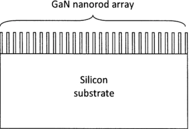
Currently, commercially available white LEDs are generally made of blue GaN LEDs added with phosphors. The focus of this thesis will be the development of new materials morphologies (rods) and specifically new materials. A focus on traditional GaN is therefore the natural choice. A novel structure for an LED is represented in Figure 2. A silicon substrate is used with a GaN
nanorod array. The silicon substrate serves as a platform for nucleation and growth of the nanostructures, and the nanorod array is responsible for light generation. The next section will explain the motivation for utilizing this structure.
GaN nanorod array
Silicon substrate
Figure 2 - Sketch of the novel LED structure.
1.3. Motivation to using nanorods
It is clear to the research world that when things become small (to micro- or nanoscales), their properties usually deviate from those of bulk materials. They can have improved mechanical strength [8], changed electrical behavior [9] or become superhydrophobic [10]. This deviation from the usual bulk material properties is the main reason why many material scientists' research interests are in micro- or nanoscale structures. In semiconducting materials, the main incentives for forming nanorods are achieving quantum confinement and lower defect densities.
1.3.1. Quantum confinement
Quantum confinement occurs because electronic energy levels change when the size of the structure is reduced to the nanoscale. This phenomenon can be explained by quantum mechanics. When structures become sufficiently small (exciton Bohr radius of GaN is 11 nm [11]), the allowed quantum states can no longer be taken as continuous but as discrete levels. The smaller the structure, the further separated in energy each discrete step will be, which in turn increase the band gap. Akiyama et al. has recently calculated that GaN quantum wires indeed have increased band gaps (estimated to be increased to 4.7 eV for nanorods with 1.3
1.3.2. High quality crystal
Nanorods also have a very important advantage for electronic devices, which is the ability to create high quality single crystal semiconductors. When forming an epitaxial layer of material, different from the substrate, it is important that the lattice constants match or at least do not differ too much, if low-defect epitaxial growth is desired. In cases of non-matching lattice constants, dislocations appear when the layer exceeds a certain critical thickness [13, 14]. Dislocations reduce the performance of LEDs, because they lead to carrier traps and reduce efficiency.
The nanoscale diameter of rods makes it less likely for dislocations to form, even in heterostructures, for several reasons.
The reduced dimension of a vertical nanorod means only a small area is in contact with the substrate. Hence, only a small base area of the new material is forced to align its lattice to the lattice constant of the substrate. The rest of the rod will be able to elastically relax in radial directions [15]. A small base area will also mean a great reduction of threading dislocations occurring at the interface, thus minimizing the formation of misfit dislocations initiated by threading dislocations [16].
The small diameter of a nanorod also makes it difficult for dislocations to nucleate within the rod. Matthews et al. showed that nucleation of half-loops requires a critical radius before it can be formed [1]. If the nanorod could not accommodate half-loop of at least the critical radius, it is reasonable to think that half-loop nucleation would not be possible according to Matthews et al.'s theory.
J7rJ.lL
I /
I I /
I I L I
(a) (b) (c)
Figure 3 - Stages of nanorod growth to remove threading dislocation. Adapted from reference [1].
The high aspect ratio of a nanorod also discourages the presence of dislocations. According to Matthews et al., if there exist a threading dislocation in the interface, growing a film beyond a certain critical height will initiate gliding of the threading dislocation (see Figure 3) [1]. However, as threading dislocations are usually inclined at an angle to the substrate surface (the (111) slip
plane is 54.70 from the conventional (001) plane substrate), the high aspect ratio of nanorods
will avoid having threading dislocations affecting most of the nanorods crystal [17]. Referring to Figure 4, it can be seen that dislocation only affect near the base of a nanorod, while keeping the rest of the nanorod defect free.
Part unaffe by threadin dislocations Part affectE by threadin dislocation! le between plane and strate surface
Figure 4 - Schematic of how threading dislocations do not affect the defect density of a nanorod beyond a certain aspect ratio. Adapted from reference [17].
1.3.3. Geometrical advantage in light extraction
The nanorod form also provides a geometrical advantage in light extraction of an LED. Light
extraction is often an issue in LEDs, where a percentage of radiated light could not escape out of the semiconductor. The cylindrical rod shape allows light to escape through the sides at all angles around the rod.
1.4. Motivation for using silicon substrates
Currently, only expensive substrates like sapphire, silicon carbide (SiC) or GaN wafers are used for growing of GaN-based devices. This is due to the lack of cheap substrates which have matching lattice constants with GaN. The high cost of substrates substantially increases the
production expense of GaN-based LEDs.
In comparison, silicon is a much cheaper alternative as a substrate. Sapphire wafers cost about
US$40 per 2" wafer. SiC substrates are even more expensive, commanding a price of US$320
per 2" wafer. On the contrary, a 2" silicon wafer is priced at less than US$10. These prices are quoted from University Wafer's website [18]. Silicon is very abundant on earth, mainly found in the form of sand (silica); hence, even a widespread use of silicon is unlikely to affect the price
stability of silicon. In addition, there is unlikely to be any shortages of silicon which could impede the production of the proposed devices.
In addition, due to the maturity of the silicon chips industry, silicon production techniques are
wafers, where only 4" wafers are produced for sapphire and SiC. Other than having larger wafer size, a lot of fabrication techniques are already available and widely practiced commercially.
1.5. Commercial viability
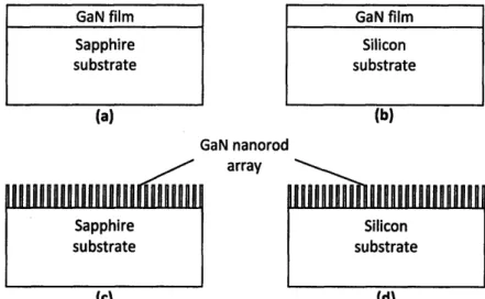
The current platform of GaN-based LED structures is planar thin films grown on sapphire substrates. Having looked into the motivations, an important question to ask is if it is advantageous to replace the existing technologies with GaN nanorod structures and silicon substrates. Does the new structure have significant improved performance and lower cost that entail an important change in white LED structures?
(a) (b)
GaN nanorod
array
(c) (d)
Figure 5 - Possible LED structures. (a) GaN film on a sapphire substrate. (b) GaN film on a silicon substrate. (c) GaN nanorod array on a sapphire substrate. (d) GaN nanorod array on a silicon substrate.
To be absolutely certain of the benefits of a GaN nanorod arrays on a silicon substrate structures have over GaN thin films on sapphire substrates, we should have a stepwise comparison. With this in mind, four structural designs of GaN-based LEDs are considered for their commercial viability [19]. The first design is the current GaN thin film on sapphire substrate structure; the second design is GaN thin films on silicon substrates; the third design is
GaN nanorod arrays on sapphire substrates; and the final design is GaN nanorod array on a
silicon substrate (see Figure 5). The goal of this thesis is to evaluate the relative advantages of these four structures.
GaN film Sapphire substrate GaN film Silicon substrate
111II1111I
i O0
11i00MR111
Sapphire substrate Silicon substrate2. Competing Technologies
In order to explore the commercial viability of a new GaN-rod-based LED structure, it is important to consider other competing technologies for the same purposes of general illumination. We will consider state-of-the-art white LEDs, organic LEDs (OLEDs) and incumbent lighting technologies (incandescent and fluorescent lamps).
2.1. State-of-the-art white LEDs
Currently, the state-of-the-art white LED is made up of thin films of GaN and InGaN to produce blue light, and incorporating phosphors to achieve white light. The phosphor used is typically cerium-doped YAG (Ce3+:YAG). This phosphor absorbs blue light and has an emission spectrum from around 500 to 700 nm. Manufacturing variations and varying thicknesses enable LEDs to produce light with different color temperatures.
Figure 6 - Schematic structure of the state-of-the-art GaN-InGaN LED on a sapphire substrate. Derived from reference [20].
A sapphire substrate is used, and a low-temperature GaN (LT-GaN) buffer layer is grown on top
of the substrate. The LT-GaN buffer layer is necessary to form a continuous film initially [21], before more layers can form on the substrate. A pn junction made of GaN is then deposited on the buffer layer. Active layers are usually constructed of multiple quantum wells (MQW) of InGaN sandwiched between the p-type and n-type GaN (see Figure 6). This active region is responsible for light emissions.
Commercially available white LEDs often suffer from low light extraction due to total internal reflection of generated photons. Reflected photons are trapped inside the semiconductor and reabsorbed by the device. Other than light extraction problems, the use of a lattice mismatched
sapphire substrates causes a high dislocation density in GaN layers. A new technique, epitaxial lateral overgrowth can be used to reduce the dislocation density, but the dislocation density is still high at 106 cm-2 [22].
Currently, Nichia Corporation, one of the leading LED companies which is based in Japan, claim to have developed white LEDs with a high luminous efficacy of 150 lumens per watt [23].
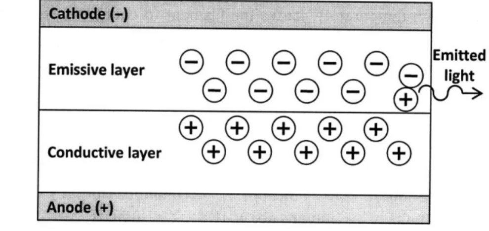
2.2. Organic light emitting diodes
OLEDs actually have very similar working principles as conventional LEDs. The difference is that
OLEDs uses films of organic compounds like tris(8-hydroxyquinolinato)aluminum [24], instead of inorganic materials like gallium arsenide (GaAs).
Emissive layer
(0
(
( 0
Conductive layer
(
Emitted light
Figure 7 - Schematic diagram of an OLED.
The cathode and anode serve as contacts for application of voltage. When an electrical potential is applied, the positive anode draws electrons from the conductive layer and repels holes towards the emissive layer. For the emissive layer, the negative cathode repels electrons in the emissive layer away from it and towards the conductive layer. Eventually, the electrostatic force will bring the electrons and holes together and they recombine in the emissive layer, generating light (see Figure 7). Similar to inorganic LEDs, only forward biasing can cause light emission from an OLED.
OLEDs have one main advantage over LEDs: they can be produced at much lower cost.
Polymer-based OLEDs can be fabricated fairly cheaply using spin coating even on flexible substrates [20].
For LEDs, the substrate must be crystalline and lattice-matching to minimize dislocations, or efficiency will be greatly reduced. More importantly, substrates suitable for GaN-based LEDs are expensive. OLEDs are better than LEDs in terms of cost.
As of today, OLEDs still lose out to LEDs in efficiency. According to Universal Display Corporation,
is much lower than LEDs' 150 lumens per watt. In terms of lifetime, LEDs still have an edge over OLEDs. Osram Opto Semiconductors have claimed that their OLEDs have lifetimes of greater than 5,000 hours [26], but this is still lower than the LED's projected lifetime of 10,000 hours. In short, OLEDs are possible candidates for general illumination due to their low cost of production. However, their low efficiency places them at a disadvantage with respect to LEDs. Unless OLED efficiency is improved to be at least comparable to LEDs, OLEDs are unlikely to supersede LEDs as the devices for SSL.
2.3. Incumbent lighting technologies: fluorescent & incandescent lamps
Light generation from incandescent and fluorescent lamps has innately different mechanisms from SSL. An incandescent lamp works by electrically heating a filament, which results in high temperatures. The high temperature causes the filament to emit light. For fluorescent lamps, light is not created from heat but from inelastic scattering of electrons that occur when electricity is applied to gases enclosed in a glass vacuum chamber. Collisions between electrons and atoms bring the atoms to excited states, and ultraviolet light is emitted when they revert back to the ground state. This emitted ultraviolet radiation in turn excites fluorescent coatings in the lamps, emitting visible light.
Cost per luminous Lifetime / Efficacy / Luminous Output / Cost per luminous
Lamps hours lumens per watt lumens $kilolumensoutput /
$/kilolumens
Incandescent 750 - 12,000 15 - 25 = 850 0.30
Fluorescent 7,500 - 24,000 55 - 100 = 5,300 0.60
White LED 50,000 88 45 25.00
Table 1 -Typical performance and cost of incandescent, fluorescent and white LED lamps. Note that the white LED has much lower efficacy than laboratory prototypes. Figures from references [3] and [27].
Efficacy is a ratio of useful light power emitted to the applied electrical power. The useful light, measured in lumens, is adjusted to average human eyes' sensitivities to different wavelength of light. One lumen is equivalent to the amount of light received on a square foot of area that is illuminated by one foot-candle. The luminous output is the total amount of useful light, in lumens, produced.
Both incandescent and fluorescent lamps do not have better lifetime or efficacy than LEDs. However, it should be noted that fluorescent lamps still have comparable efficacy (see Table 1).
In addition, they are superior in terms of cost per luminous output.
Other than costs, these incumbent lighting technologies have already formed a solid foundation among consumers. Contractors who install lighting for buildings will naturally choose options
with lower installation costs and that are known to be reliable. As the savings of electricity is not enjoyed by contractors who choose which lighting to install, unless users specifically state that they want LED lighting, contractors are unlikely to use LEDs instead of incandescent or fluorescent lamps. It would be difficult to convince the market to replace technologies which have been working well for many decades with another more expensive technology. Hence, only a technology with tremendously improved performance can stand a chance to replace these incumbent technologies.
3. Proposed Device
GaN rods
SOG
Light Contact pad Active layer--Transparentelectrode
Figure 8 - Proposed design of an LED structure. (a) Top view of GaN nanorod array. (b) Schematic cross-sectional view of proposed LED structure.
A preliminary design of the LED is proposed (see Figure 8). This design resembles that shown in (d) of Figure 5, adopting changes motivated by the earlier discussion. Silicon is chosen to be the
substrate of choice, and vertical GaN nanorods are to be grown on top. The GaN nanorods are constructed to form pn junctions. The active layer is the region where emission occurs, and could be formed by a superlattice of InGaN, sandwiched by wide band gap aluminum gallium nitride (AIGaN). Spin-on-glass (SOG) is proposed to fill up the gaps between the nanorod array so as to provide a mechanical support for the rods. SOG can also serve as a passivation coating for the nanorods.
aN
rods
Contact
pad
4. Nanofabrication of Nanorods
In this thesis, the nanostructure of interest is a nanorod, or more specifically, a periodic arrangement of vertical nanorods with axes normal to the surface of a flat surface. There are several methods for growth of such structures of GaN. Approaches such as template synthesis [28], catalyst-assisted vapor-liquid-solid (VLS) [29] and nanocapillary condensation [30] are proven to be plausible approaches to growth of GaN nanorods.
4.1. Template synthesis
In template synthesis, nanostructures of the desired material are grown by making use of a membrane with pores of uniform diameter. The membrane is then removed, leaving behind the desired nanostructures. Usually, the pores will have cylindrical shapes which the desired material would follow. Even with only cylindrical shapes, there is still some flexibility in forming nanostructures with the materials of interest, like nanodots [31], nanorods (or nanowires) [32], nanotubes [33], and even nanorings and nanoarrows [34].
Anodized aluminum oxide (AAO) has several advantages as a template membrane. AAO is a self-assembled membrane with vertical nanopores arranged in a triangular lattice. It is cheap to produce as only electrochemical oxidation is required and its pores are self-organized. In addition, among template synthesis, high porosity AAO is one of the mostly researched
membranes [28]. Since AAO has the potential to produce cheap and high density nanorod arrays, it is selected as the choice for nanorod synthesis.
4.1.1. Formation of AAO membrane
For the formation of ordered AAO, a two-step anodization process is adopted. This is to attain better ordering of the pores [35]. When a flat surface of aluminum is anodized in a weak acid environment (either diluted oxalic, sulfuric or phosphoric acid), pores nucleate randomly, usually in a disordered manner. These pores will extend into the aluminum, forming thicker
AAO with distorted pores. Given enough time, however, the pores will eventually form ordered hexagonal arrays deeper into the AAO. The AAO can then be removed using a mixture of phosphoric acid (6 wt %) and chromic acid (1.8 wt %) [31]. What is left behind is an ordered array of nano-indents whose position and size reflect that of the removed AAO pores' positioning and size at the interface between AAO and aluminum. The second anodization is then done, and pores form according to the ordering of the nano-indents.
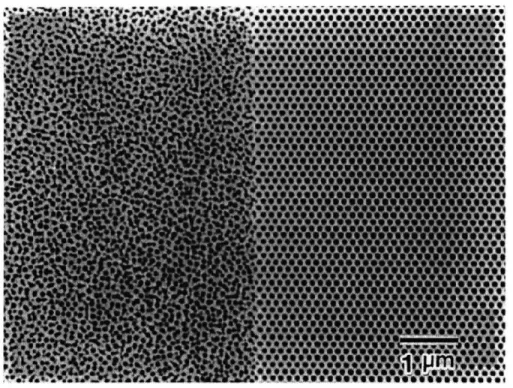
It should be noted that the resulting arrays of pores are only ordered at short-range. If long-range order is desired, pre-patterning of the aluminum should be done before anodization.
Masuda et al.'s experiment illustrated the differences in ordering between an AAO surface that was pre-patterned and one that was not (see Figure 9).
Figure 9 - SEM images of AAO surfaces. Right: the AAO is anodized after pretexturing with a SiC mold by mechanical molding. Left: the AAO is untextured. Image adapted from reference [36].
It is possible to adjust the pore size and separation through the anodization conditions [37, 38]. This ability to modify the pore size and periodicity allows flexibility in creating nanorod arrays optimized for LED purposes. In addition, it is also possible to control the pore separation distance by pre-patterning the aluminum film with periodic indents using interference lithography [39] or mechanical molding [36]. This pre-patterning not only provides long-range ordered pores, it could even produce an ordered square lattice of pores (see Figure 10).
After forming porous AAO on a substrate, pore widening must be done. This is to increase the pore size to the required diameter and also to open the barrier layer at the base of AAO. Once the AAO is formed either pattern transfer of pores [40] followed by deposition or direct deposition [41, 42] of the material of interest is done. There are several methods for deposition of materials, including evaporative deposition, chemical vapor deposition (CVD) and electrochemical deposition. Usually for direct deposition, electrochemical deposition is done. However, electrochemical deposition can only be used to deposit materials on a conductive surface. Therefore, it is not used for deposition of GaN on the conventional insulating sapphire substrate. Nevertheless, it is still possible to grow GaN on silicon substrate using electrochemical deposition, but it is suggested that quality suffers as both hexagonal and cubic phases of GaN are obtained [43].
Figure 10 - SEM images of long-range ordered arrays of pores in AAO arranged in a square lattice, possible through pre-patterning. Adapted from reference [39].
4.1.2. Deposition to form GaN nanorods
Usually when growing a binary material like GaN on a single element substrate (like silicon), precaution should be taken to prevent formation of antiphase domains. In a single-crystalline material, there exists a periodic arrangement of atoms which has to be consistent throughout the grown layer. In a compound material (i.e. AB), this consistency could be easily lost when the elemental arrangement is not perfect (i.e. A-B-B-A). Hence, it is difficult to grow a single-crystal layer of a compound semiconductor over a large area, especially when the substrate is of a single element (Si). However, growing of nanorods tends to avoid this issue. This is because each nanorod should be a single crystal of its own, without the need to synchronize atomic arrangement with the rest of the rods. The much smaller base area of nanorods allow only one nucleation per nanorod [44].
4.2. Catalyst-assisted vapor-liquid-solid
VLS is a nanofabrication method where the material of interest is initially in its vapor phase,
usually in a compound form. Liquid catalysts, usually metal, of nanometer length scale, are decorated on the substrate surface. The gaseous precursor will first adsorb preferentially on the liquid catalyst rather than the substrate's surface. Subsequently, dissociation into the required material is catalyzed by the presence of liquid catalyst, forming a single phase solution.
As more material is adsorbed, the liquid catalyst eventually becomes saturated and the material starts to precipitate. The precipitated material will adhere to the substrate, forming a crystalline solid. The resulting structure is a rod shaped structure which takes the shape and size of the liquid catalyst. All nanorods formed by VLS have a characteristic blob of metal catalyst on one end.
Figure 11 - Schematic of the catalytic VLS process for growth of nanorods. Adapted from reference [45].
There are several choices of catalyst to make GaN nanorods, including iron, nickel and indium. Although gold is commonly used as a catalyst in VLS, it is not suitable for growth of GaN nanorods or nanowires [46], due to poor solubility of nitrogen in gold [47]. Nevertheless, it is still possible to grow GaN nanorods using gold catalysts on silicon substrate [48, 49]. Both Cao et al. and Yu et al. managed to grow GaN nanorods with diameters ranging from 50 to 80 nm. However, GaN nanorods failed to form when the gold catalyst droplets exceeded a certain size [48].
Since the nanorods are grown using a catalyst, it is possible that they have traces of the metal catalyst in them. Inclusion of such material could be disastrous for LED applications. In order to avoid the possibility of unintentional contamination, we should avoid using VLS to construct structures for LEDs.
4.3. Nanocapillary condensation
Seo et al. described an interesting way to grow nanorods out of GaN, which is by capillary condensation [30]. Unlike VLS, capillary condensation does not require the presence of a catalyst to start growth of nanorods. This method is interesting because it makes use of self-assembled nanotrenches, which are formed during coarsening of GaN islands in a lattice-mismatched system [30]. The GaN is grown using plasma assisted molecular beam epitaxy (MBE). This creates several voids or nanotrenches in the layer of material. From these nanotrenches, Ga atoms nucleate in them and start to grow upwards, forming arrays of GaN
Precursor gas
Liquid Precursor gas g
catalyst
Cluster
Nucleation
:
a I ..
_-formation and growth Nanorod
11
11111111131
P
···-·-·-····-·---·---1:·- --- ·-··--··-···-···-·Yla*lr*,
nanorods. The GaN layer containing trenches serves as a mask for the GaN nanorods to grow, similar to the mechanism of an AAO template.
Figure 12 - SEM of GaN nanorods grown by nanocapillary condensation. (a) GaN nanorods protrude out of the nanotrenches. (b) Cross-sectional view of a GaN nanorod. (c) Top-view of a GaN nanorod. From reference [30].
It should be noted that the nanorods protrude out of the film due to a faster vertical growth rate than the rest of the film. Eventually, the rods will grow at the same rate as the surrounding film after they grow out of the trenches. Hence, the nanorods could only be of a certain height above the film surface by this method of fabrication. In addition, the nanorods only populate the surface sparsely.
5.
Proposed Fabrication Procedures
In consideration of the ability to grow high density of monocrystalline nanorod arrays with simple controllability of rod size and separation, the template synthesis of nanorods using templated AAO is chosen as the fabrication method.
Si substrate with SiO2 Deposition of Al Anodize to form AAO
Transfer pattern to SiO2 MOCVD growth Remove SiO2
Apply SOG Complete with contacts pads and electrode Figure 13 - Fabrication steps.
First, start with a silicon wafer as substrate with a layer of silicon dioxide (SiO 2) already on top
of it. The SiO2 could either be deposited by electron beam deposition or formed by oxidation of
the silicon wafer. Next, deposit a layer of aluminum on top of the SiO2 by electron beam
deposition. After that, do a two-step anodization process described previously. Anodization should be done to ensure a complete conversion of aluminum to AAO. Next, perform pore widening by immersing AAO into diluted phosphoric acid solution at room temperature [50]. The aim is to widen the pores to the required diameter and also to open the barrier layer at the
bases of the pores.
Now, transfer the pore array pattern to the underlying SiO2 using inductively coupled plasma
(ICP) etching, and remove the AAO by immersing it into diluted phosphoric acid solution at
elevated temperature [50]. Removal of AAO is necessary as GaN readily nucleates on it, but not
on SiO2 [50], thereby providing selective epitaxy [22] conditions. GaN nanorods are grown using
the MOCVD method. The SiO2 is then removed to get the GaN nanorod array.
Lastly, apply a spin-on-glass (SOG) to the GaN nanorod array to provide the rods with mechanical support. After that, contact pads and electrodes can be incorporated into the device structure.
6. Comparative Advantages
From the motivations in the earlier part of this thesis, it can be seen that that are several advantages that could be derived from the use of nanorod arrays and silicon substrate. However, an important question follows the motivations: does the new structure have significant improved performance and lower cost that entail a revolutionary change in the fabrication of white LED structures? Hence, a comparison of the derived advantages of the four
distinct structure designs listed in Figure 5 is necessary.
6.1. Lower costs
Silicon substrates are not used as the substrate for current GaN LEDs, because of the large lattice mismatch between silicon and GaN. This mismatch will produce a high density of dislocations and defects in the device, which lowers its efficiency greatly. Hence, a more lattice matched substrate, sapphire, is currently being used for commercial white LEDs.
In this new technology, nanorods are being grown instead of thin films. This greatly decreases the contact the grown material has on the substrate. Therefore, a large mismatch (i.e. between GaN and silicon) could even be accommodated elastically. Even if there are threading dislocations, they would be at a low density.
Typically, a 4" sapphire wafer costs US$250, whereas a 12" silicon wafer costs around US$20. This means that using silicon substrate is more than 100 times cheaper than using sapphire substrate in terms of cost per area. In addition, current technology can only produce sapphire wafers up to 4", whereas silicon wafer could reach 12". The bigger wafer size of the silicon allows more devices to be fabricated per step than the smaller wafer size of sapphire. This translates to great cost savings for this technology. However, the cost of equipment for handling of 12 inch wafers significantly exceeds the cost of equipment for 4 inch wafers. This has not been accounted for in subsequent analyses.
However, additional costs might be derived from the extra fabrication steps. The increased complexity in fabrication is likely to increase costs associated with more inspection tests and lower yield. But it is unlikely to negate the savings from the substrate cost.
Referring to Figure 5, a ranking of the four designs in terms of cost would be (b), (d), (a) and (c), in descending order.
6.2. Yield & reliability
When using GaN nanorod arrays as LEDs, it can be seen as arrays of individual LEDs working in parallel to make a single device. This can result in improved reliability.
Each nanorod is a single LED on its own. Therefore, break down of the whole device is less likely, as malfunctioning would mean all nanorods have to fail at the same time. The failure of one
nanorod is unlikely to affect others as they are segregated from each other. This is not the case in the incumbent thin film technology. Hence, having nanorod array structures tends to reduce the number of device failures. This improves the reliability of the device.
To show this mathematically, we shall assume that after a year of operation, 5% of all LEDs will fail. Hence, it would mean that for conventional LEDs, only 95% of them will be functional after a year. However, if this 5% failure rate is applied to nanorod array LEDs, these devices will work with 95% brightness (95% of the nanorods working) after one year, but 100% of them would be
working. This translates to higher reliability. Although this is a rather simple perspective, it provides a reasonable logic to help us understand how reliability is improved.
Other than considering the failure rate, reliability is also improved because of the lower dislocation and defect density in nanorods. Yield would probably be better with the lower defect density. Seo et al. [51] have reported negligible defects in GaN nanowires (25nm diameter) grown on silicon substrates.
However, lower yield can result from the greater complexity and number of fabrication steps to create nanorod arrays. There are 6 more fabrication steps for the new structure than the conventional thin film structure. Every fabrication steps will contribute to a yield loss, as every step has a probability of reducing the yield of the output; hence, the increase in number of steps is detrimental to the overall yield. This yield loss is an uncertainty, as of now, which could only be known after production of GaN nanorod arrays using AAO is industrially optimized.
Referring to Figure 5, a ranking of the four designs in terms of yield and reliability would be (c),
(d), (a) and (b), in descending order, considering if the yield loss due to the additional AAO step
is not significant. Note that designs with sapphire substrates tend to have better yield and reliability because of the lower lattice mismatch.
6.3. Higher efficiencies
Efficiency is very important in the working of LEDs. This is because one of the main reasons for
LED to replace incumbent lighting technologies is their improved efficiency. Higher efficiency
can result from higher quality crystals, cylindrical structures of nanorods, and, possibly, through photonic crystal effects.
Higher efficiencies are derived from the better quality of GaN grown. The reduced dislocation and defect density attributed from the nanorod structure enhances the internal efficiency of the device. The explanation for how dislocations and defects can be reduced has been given earlier in this thesis. Dhariwal & Ram have recently shown that small size can reduce the non-radiative recombination [52], which in turn would enhance non-radiative recombination.
There should be an optimal, or at least a maximum, diameter for the nanorods, in which dislocation density is kept at a minimum. We can obtain an optimal (or maximum) diameter by considering the lattice parameter and thermal expansion coefficient mismatch. The lattice parameter of GaN is 3.186 A and for silicon is 5.431 A. From these values, we can calculate the distance between each dislocation (Ld = asubaep ), neglecting elastic accommodations.
Aa
Dislocation density would be minimize if diameter of the nanorods is less than Ld. However, the calculated Ld is 7.707 A, which is too small to form nanorod structure.
Next we look at the thermal expansion coefficient mismatch. Thermal expansion coefficient for for GaN is 5.6 x 10⁻⁶ OC1 and silicon is 3 x 10⁻⁶ OC-1. Since growth is done at above 1,000 OC, the difference in thermal expansion should result in a mismatch of around 2.6 x 10⁻³ in strain. To avoid defects which arise from this thermal expansion mismatch, the mismatch in expansion should probably be less than half the lattice parameter of GaN, and this gives a diameter of
around 61 nm. With that, it can be derived that the nanorod diameter should be less than 61nm.
The geometry of nanorods also provides better light extraction than the incumbent thin film structure. Instead of the usual light extraction through the top in thin film technology, light could escape through the sidewalls of the nanorods. This provides a greater area for light to escape from the semiconductor, enhancing the extraction efficiency. Kim et al. [53] have reported a 4.3 times improvement in light intensity in nanorods LEDs compared to conventional thin film LEDs. This shows that although nanorod arrays have inherently smaller active regions than thin film semiconductor, their light output can still exceed that of the planar film technology.
A periodic array of nanorods can function as a planar photonic crystal, or photonic crystal rod
slab. This structure behaves as a waveguide for light moving in the direction perpendicular to the substrate, by having a photonic band gap in the planar directions. This means that light can be directed to be extracted more efficiently, because lateral propagation of guided modes is forbidden. Adjusting the nanorod array's period and size could change the structure to guide the desired light wavelength, which is 450 nm. Several research groups [54-56] have claimed the effectiveness of photonic crystal in improving LED performance.
Referring to Figure 5, a ranking of the four designs in terms of efficiencies would be (c), (d), (a) and (b), in descending order.
6.4. Overall comparison
The ranking made in the previous sections is consolidated below for a better comparison (see Table 2).
Ranking (a) Film on a (b) Film on a (c) Nanorod arrays (d) Nanorod arrays
sapphire silicon on a sapphire on a silicon
substrate substrate substrate substrate
Cost 3 1 4 2
Yield &
3 4 1 2
reliability
Efficiency 3 4 1 2
Table 2 - Consolidated ranking order of the four LED designs from Figure 5, with 1 being the best.
Although (c) is better than (d) in both yield & reliability and efficiency, the improvement is not significant. This is because the nanorod structure already compensates for the large lattice mismatch; hence, having a smaller mismatch (in the case of (c)) would not improve much. In addition, the improved efficiency is because of the nanorod structure, rather than the use of a better lattice matched substrate.
On the contrary, lattice mismatch poses a more serious problem in planar film technology. This is because the whole substrate area is in contact with GaN at the heterojunction, and dislocations will form easily under lattice mismatch. Therefore in (b), GaN films on silicon substrates, serious dislocation issues are expected and this will affect the reliability and efficiency to a large extent. Lei et al. have tried growing GaN films on both silicon and sapphire substrates, and their group concluded that GaN films on silicon (001) substrates are structurally worse than GaN films on sapphire substrates [57].
From the discussion above, it is clear that (a) is preferred over (b) in terms of performance. In addition, if it is possible to produce LEDs of acceptable performance using GaN films on silicon substrates, the industry will not choose sapphire substrates, which cost around 100 times more, to fabricate LEDs. From Table 2, (d) is better than (a) in the three aspects, so we are left with design (c) and (d). As discussed previously, the improvement in performance of (c) over (d) is
7. Patent Research
An intellectual property research is necessary to find out if there is any patent infringement in this technology. There exist hundreds of patents in the field of LEDs, from which only a few are relevant to this technology. Three of the patents are as reviewed.
7.1. US 7,132,677: invented by Hwa-Mok Kim, Tae-Won Kang &
Kwan-Soo Chung
"Super bright light emitting diode of nanorod array structure having InGaN quantum well and method for manufacturing the same" [58].
Figure 14 - Design of Patent 7,132,677.
This invention is very similar to the proposed design (see Figure 8). It consists of GaN-based nanorod array to create LED too. However, a major difference lies in the substrate material. This invention still uses sapphire substrate with a GaN buffer layer. In this aspect, the proposed design is superior in terms of the possible cost savings derived from the lower substrate cost, and also the elimination of the GaN buffer layer.
7.2. US 7,294,862: invented by Jonathan J Wierer, Michael R Krames &
Mihail M Sigalas
"Photonic crystal light emitting device" [59].
100
124
120 ' ` '1"_
Figure 15 - Design of Patent 7,294,862.
This invention utilizes the photonic waveguide concept, which is similar to the proposed design. However, the structure is fabricated by etching deposited thin films to form the photonic crystal structure. This method did not exploit the epitaxial growth nature of nanorods, hence their invention did not solve the defect density issue. In addition, this invention uses sapphire,
SiC or GaN substrates, which are all more expensive than silicon.
7.3. US 2007/0158639: invented by Chien-Cheng Yang, Zhi-Cheng Hsiao
& Gen-Wen Hsieh
"Substrate-free light emitting diode and fabrication method thereof" [60].
Figure 16 - Design of Patent 2007/0158639.
This invention attempts to reduce cost by introducing a substrate-free LED. However, this invention still suffers poor light extraction like the incumbent thin film technology due to lack of nanorod's sidewalls for photons to escape the structure.
8. Business Model
8.1. Market size
Technologies Total Lamps in US (millions) Percent of Lamps
Incandescent 4,397 63%
Fluorescent 2,473 35%
HID 105 2%
Solid-State 2 0.03%
Total 6,977 100%
Table 3 -Total lamps in US in 2001. Retrieved from reference [3].
According to a market survey in 2002 [3], solid-state lighting currently accounts for 0.03% of the total lamps installed in US in 2001 (see Table 3). In 2007, around $330 million of sales of high-brightness (HB) LEDs are attributed to illumination purposes. This figure is likely to increase rapidly as incumbent lightings are replaced by LEDs, where there are about 7 billion lamps to be replaced in US alone.
8.2. Supply chain
F!II
ii
II
II
II
II
Figure 17 - Supply chain of existing LED industry. Boxed area represents the participation of most dominant LED
The supply chain of the white LED market can be described by the flow chart shown above (see Figure 17). The bottom of the supply chain starts from the material (substrate), followed by fabrication, packaging, distribution, then to customers. The main players in this industry are dominated by a few companies, namely Osram, Lumileds, Cree, Nichia and Toyoda Gosei. These five main players typically participate in several stages of the supply chain. They usually engage in fabrication, packaging and distribution (see dotted box in Figure 17).
The white LED industry has been around for more than 10 years, ever since the first white LED was invented and commercialized in 1996. Although this was not a long time relative to other industries, it is long enough for the supply chain to establish a stable relationship between the material suppliers and the customers. Material suppliers gained trust in the main companies, as they are confident that there would be sustained business between them. On the other end, customers also felt these main companies have product assurance due to their reputation in the industry. Hence, this industrial environment is difficult to penetrate into.
8.3. Business plan
Ir
II
II
II
II
II
Materials SiliconII
Ii
II
II
)I
Licensing AluminumFigure 18 - Proposed changes to the existing LED supply chain.
The market penetration plan is to have a partnership with one of the major players in the white
LED industries. In this way, it will be easier to enter the market with minimal capital investment.
Market risks would be lower as the products are marketed under an established brand. In addition, a relatively large market share can be enjoyed in a short period of time.
The difficulty in convincing the major companies to collaborate should not be high. Firstly, the
LED industry is very open to innovations, due to the high competition between LED companies
to outperform each other in their technologies. There is an ongoing race between the companies to produce the technology to the most efficient LED. This provides a suitable ambiance for technology companies to thrive. In addition, the proposed LED design comes with three very attractive advantages all in one package; namely lower costs, higher yield and higher efficiencies.
An optimal business plan would be for us to fabricate the LED chips, and then license the major company for sales. Ideally, packaging and distribution should be assigned to the major company as it already has the infrastructure ready.
A partnership could be established with Osram, for example, who enjoyed sales of about $97
million in its optical semiconductor sector. With reference to Figure 18, it is proposed to provide the device fabricated until the SOG step (see Figure 13). Subsequent steps should be similar to the current technology, hence we could take advantage of Osram's existing facilities for the rest of the fabrication, and also the packaging. We could settle for collaboration, based on the proposed technology's competitive advantages. The competitive advantages of the proposed technology should be attractive to these major companies because of the strong competition in the industry.
8.4. Returns projections
A simple estimation of the returns could be calculated as such.
Currently, Osram is producing 1,000 square meters of wafer area and having $97 million sales in optical semiconductors yearly [61]. It shall be assumed that if a partnership was formed with Osram, 1% of their sales would be allocated to us. Our sales would equate to $970,000, with production at 10 square meters of wafer area per year. This translates to around 1273 of 4" silicon wafers per year.
Estimating a labor requirement of 4 workers ($25/hour for 250 days per year, and at 8 hours per day) for operations, building rental of $200,000 per year and a simplified combined cost of
$50 per wafer for raw material, fabrication, we obtained an estimated yearly cost of $463,662.
With regards to the revenue allocation, I propose getting 35% of the final sales revenue, or
$339,500, to be allocated to the new operation (arbitrary estimation).
Taking 35% of the final sales revenue is reasonable. Assuming that all optical semiconductors sold by Osram use 4" sapphire wafers as substrates, 1,000 square meters of wafer area will require about 127,000 4" sapphire wafers, or about $760 of sales per 4" sapphire wafer. Since
each 4" sapphire wafer costs $250, almost a third of the sales revenue is to cover just the substrate cost, excluding any fabrication costs. In other words, Osram would still enjoy cost reduction even if 35% of the sales revenue is allocated to us.
Further assuming a 10% increase in the total market share and another 10% increase in the allocation of total sales from the major company (Osram), a 5-year returns projection can be computed (see Table 4).
Fabricated Wafer Cost 63,662 77,031 93,208 112,781 136,465 483,147
Wafer Cost ($)
Labor and Rental an$) 400,000 400,000 400,000 400,000 400,000 2,000,000 Renta ($) -124,162 -66,236 3,854 88,664 191,283 93,404 Profit ($) -124,162 -66,236 3,854 88,664 191,283 93,404Table 4 - Profit projections over 5 years of manufacturing, taking 1% of Osram sales.
A loss will be suffered in the first two years, before profit is enjoyed from the third year onwards. This would not be ideal as although there is an overall profit enjoyed over the 5 years, it is insufficient to cover for equipment and capital costs (around $250,000). Hence, we should secure a higher proportion of Osram's sales at 2% (see Table 5).
Fabricated Wafer Cost 127,324 154,062 186,415 225,562 272,930 966,293
Wafer Cost ($)
Labor and
Rental 00 4400,000 400,000 400,000 400,000 400,000 2,000,000 Profit ($) 151,676 267,528 407,709 577,328 782,567 2,186,807Table 5 - Profit projections over 5 years of manufacturing, taking 2% of Osram sales.
The production level at the end of 5 years is around 5,500 wafers per year, or 22 wafers per day, which is a reasonable production volume. Note that the labor and rental costs remain constant as it is assumed that the floor space and labor requirements are not affected by the increase in production volume. In addition, production is assumed to commence immediately upon set up. Negating the equipment and capital costs (MOCVD machine at about $55,000, evaporative deposition chamber at about $115,000, inductively coupled plasma etching equipment at about $45,000 [62] and clean room setup at about $20,000), approximately $1.94 million profit could be earned in 5 years.
8.5. Funding sources
There are several funding sources available for start ups. They are listed below: * Small business innovation research (SBIR) program
* Building Technologies Program in the Office of Energy Efficiency and Renewable Energy (EERE)
* US Department of Energy (DOE) or National Energy Technology Laboratory (NETL)
Such funding could be used to cover infrastructure and initial set up costs. The funding can also be used to cover the cost in the pre-qualification of a test laboratory to participate in DOE's Commercially Available LED Product Evaluation and Reporting (CALIPER) Program.
In addition, investment from venture capitalists is also required. Using the $0.69 million profit projection, estimated funding required from venture capitalists is around $0.5 million with a projected 18% yearly returns at the end of 5 years.
However, we should be careful to note that this is assuming that manufacturing starts as soon as the funding is received. This is unlikely because presently, there is a lack of large-scale production in such a technology. Development in production, and also further research in this technology, will take time. It would be more realistic projection for 5 years would to be having at least a year of research development, followed by four years of manufacturing.
9. Conclusion
Templated growth of nanostructures is an emerging technology with a high potential for commercialization. One viable application is solid-state lighting, due to its large potential market. Motivations in LED technology is towards cost-savings and higher performance. The use of GaN nanorod array provides performance improvement in LEDs and the use of silicon substrates are much cheaper alternatives to sapphire substrates, which are used by the state-of-the-art white LEDs. A device structure is proposed accordingly, which is GaN nanorod array on silicon substrate.
Several fabrication techniques are investigated to find out which is the most suitable for fabrication of nanorod array. The fabrication technique using AAO allows high density of nanorods to be grown in an orderly fashion, topped with controllable separation and size. In addition, AAO forms pores by self-organizing, cutting possible high costs which are incurred from lithographic means. Hence, AAO template synthesis is selected.
It is found that the proposed LED structure design (GaN nanorod array on silicon substrate) is suitable for commercialization in the LED industry, specifically for general illumination purposes. This is due to the three important competitive advantages enjoyed by using this structure;
namely lower costs, higher yield and reliability and higher efficiencies. This thesis has also looked into three other LED structure designs: GaN film on sapphire substrate (current GaN LED structure), GaN film on silicon substrate and GaN nanorod array on sapphire substrate. It has been found that GaN nanorod array on silicon substrate provides the best performance to cost for LED.
Collaboration with an existing company, preferably dominant, is crucial to commercialization of this technology. The high costs of infrastructures and high barriers to penetrating the LED supply chain greatly impede the entrance of a new company. Therefore, forming a partnership is vital to starting up a business based on this new LED structure.
As presented above, commercialization of this technology is promising. It provides cost savings while having a performance boost to the existing LED. This allows a sound business plan to be possible, with a healthy profit projection.

![Figure 3 - Stages of nanorod growth to remove threading dislocation. Adapted from reference [1].](https://thumb-eu.123doks.com/thumbv2/123doknet/14383895.506834/11.918.215.694.716.959/figure-stages-nanorod-growth-threading-dislocation-adapted-reference.webp)