HAL Id: tel-00175417
https://tel.archives-ouvertes.fr/tel-00175417
Submitted on 28 Sep 2007
HAL is a multi-disciplinary open access archive for the deposit and dissemination of sci-entific research documents, whether they are pub-lished or not. The documents may come from teaching and research institutions in France or abroad, or from public or private research centers.
L’archive ouverte pluridisciplinaire HAL, est destinée au dépôt et à la diffusion de documents scientifiques de niveau recherche, publiés ou non, émanant des établissements d’enseignement et de recherche français ou étrangers, des laboratoires publics ou privés.
molecular conductor
A. Zazunov
To cite this version:
A. Zazunov. Coherent phenomena in electron transportthrough a molecular conductor. Physics [physics]. Université de la Méditerranée - Aix-Marseille II, 2007. �tel-00175417�
pr´esent´e par
Alex ZAZUNOV
`a l’Universit´e de la M´editerran´ee
Aix-Marseille II
Sp´ecialit´e: Physique
Coherent phenomena in electron transport
through a molecular conductor
Composition du Jury
Mr. P. Dumas (Pr´esident du Jury)
Mr. F. W. J. Hekking (Rapporteur)
Mr. T. Martin (Tuteur)
Mr. G. Montambaux (Rapporteur)
Mr. B. Pla¸cais (Rapporteur)
Soutenance pr´evue le 27 septembre 2007
Ce m´emoire a ´et´e pr´epar´e au sein du
Dans cette th`ese d’habilitation, nous consid´erons plusieurs aspects du transport `a travers une mol´ecule unique, connect´ee `a des bornes de m´etal normal ou `a des bornes supraconductrices. L’emphase `a ´et´e mise sur la d´etection des signatures les plus marquantes du transport coh´erent `a travers les mol´ecules, ainsi que sur la compr´ehension des probl`emes de corr´elations (probl`eme `a N corps) sur la dy-namique de ces syst`emes, provenant des degr´es de libert´e internes (vibrations, spin, etc.) du conducteur et affectant le passage du courant.
En ce qui concerne le transport dans le r´egime normal `a travers une mol´ecule qui vibre (un nanotube de carbone suspendu par ses extr´emit´es), nous avons proc´ed´e `a une ´etude d´etaill´ee de la conductance diff´erentielle n´egative (CDN) qui est observ´ee dans ces dispositifs. En supposant des contacts tunnel, tel que les ´electrons qui s’´echappent dans les bornes effectivement perdent leur coh´erence de phase (c’est-`a-dire `a haute temp´erature), nous avons d´eriv´e les ´equations cin´etiques dans lesquelles la nature quantique de l’interaction ´electron-phonon au sein du point quantique mol´eculaire est prise en compte sans approximations (formation de polaron sur le point quantique mol´eculaire). Le fait que la con-ductance diff´erentielle soit positive ou n´egative d´epend de la position du niveau polaronique et de l’occupation des pics satellites associ´es au nombre d’occupation des phonons, qui sont compris entre la tension de source et de drain des ´electrodes. La CDN apparaˆıt lorsque deux de ces pics satellites entrent en comp´etition dans le transport, et constitue une signature des effets hors ´equilibres associ´es au vi-brations de la mol´ecule. Nous avons clairement montr´e que pour des couplages tunnels asym´etriques (situation qui correspond `a la g´eom´etrie des exp´eriences sur le domaine), on observe un CDN pour un vaste domaine de param`etres. Nous avons ´egalement explor´e les effets de navette ´electronique, ou le d´eplacement de la mol´ecule entre en compte dans l’Hamiltonien tunnel, qui peuvent ˆetre d´etect´es en regardant l’asym´etrie des courbes courant tension. Bien que le m´ecanisme de navette tend `a renforcer la CDN, il n’est toutefois pas suffisant pour y donner lieu sans hypoth`eses sur la valeur relative des couplages tunnels.
Nous avons ´egalement ´etudi´e le transport dans le r´egime normal `a travers un point quantique mol´eculaire dans le cas d’un couplage fort aux contacts, mais loin du r´egime Kondo. En utilisant l’approche hors ´equilibre des fonctions de Green dans la repr´esentation du polaron, nous sommes all´es au del`a du r´egime perturbatif pour calculer la caract´eristique courant tension dans le r´egime de
couplage ´electron-phonon interm´ediaire. Nous avons montr´e qu’en accroissant le couplage tunnel au contacts, les corr´elations associ´ees au nuage de polaron deviennent tr`es importantes `a haute temp´erature, et donnent lieu `a une r´eduction dramatique de l’´elargissement des pics la densit´e d’´etats de la mol´ecule. Nous proposons une d´etection de ces ph´enom`enes par la mesure de la conductance diff´erentielle, tout en variant la temp´erature locale de la mol´ecule (nanotube de carbone). On note qu’en pr´esence d’un environnement dissipatif les pic satellites dus aux phonons devraient acqu´erir un ´elargissement additionnel. L’inclusion des effets d’amortissement des modes phononiques constituerait une extension de ce travail.
Dans cette th`ese, nous avons ´egalement abord´e le probl`eme du transport coh´erent en pr´esence de phonons, dans un syst`eme mol´eculaire connect´e `a des contacts supraconducteurs. Nous avons calcul´e le courant DC (partie du courant stationnaire) pour toutes les valeurs de la tension `a l’aide de l’approche des fonc-tions de Green Keldysh, pour une fr´equence de vibration arbitraire, mais dans le r´egime du couplage faible ´electron-phonon. Nos principaux r´esultats sont les suivants: i) dans le r´egime sous le gap eV < ∆, les processus de r´eflexions mul-tiples d’Andreev (MAR) sont accompagn´es de processus d’´emission/absorption de phonons et donne lieu `a une structure tr`es riche pr`es des valeurs de tension ou le nombre de r´eflexions d’Andreev changent d’une unit´e (ces tensions sont ap-pel´ees les “MAR onsets”). On observe alors un effet pair impair ou le courant est augment´e/diminu´e suivant la transition de “MAR onset” (entre pair/impair et vice versa). Ces ph´enom`enes trouvent un interpr´etation physique en comparant avec la th´eorie de la diffusion de Buttiker-Landauer, adapt´ee au contacts supra-conducteurs, une th´eorie connue sous le nom d’ “´echelle de MAR”. A l’´equilibre V = 0, nous avons obtenu des r´esultats analytiques pour le courant Josephson dans la limite adiabatique ou la fr´equence de vibration est faible compar´ee au gap supraconducteur, qui est interpr´et´ee en terme des ´etats li´es d’Andreev avec une transparence aux contacts renormalis´ee par les phonons. Pour le futur, une exten-sion de cette th´eorie au calcul du bruit (fonction de corr´elation courant-courant) est envisag´ee. Le bruit peut en effet procurer une information suppl´ementaire sur la charge transmise `a travers la jonction, et il serait int´eressant d’´etudier l’effet des phonons dans ce cadre.
Nous avons ´egalement consid´er´e le cas des contacts supraconducteurs, mais cette fois pour les interactions fortes, et uniquement `a l’´equilibre ou le courant Josephson d´epend de la diff´erence de phase entre les deux supraconducteurs. Cette fois on s’int´eresse `a un diagnostique sur l’´etat des phonons sur le point quantique mol´eculaire. Nous trouvons que pour le r´egime de faible couplage tunnel, des ´etats non-classiques de type “chat de Schrodinger” (une superposi-tion d’´etats coh´erents oppos´es) sont associ´es aux ´etats du courant et donc aux li´es d’Andreev dans la jonction. Ces ´etats non classiques peuvent ˆetre explicit´es en proc´edant `a une mesure projective du courant. Pour des contacts transpar-ents, nous avons montr´e que l’effet Josephson g´en`ere des fluctuations de phonon
coh´erentes, et induit des ´etats quantiques “comprim´es” de phonon, analogues aux ´etats “comprim´es” de photons en optique quantique: l’impulsion canoniquement conjugu´ee `a la distorsion de la mol´ecule poss`ede des fluctuations inf´erieures a la valeur minimale habituelle de fluctuations du point z´ero. La compression d’´etats de phonons s’observe pour une grande plage de param`etres: elle est contrl´ee par la diff´erence de phase et devient maximale pr`es de la transition de polaron. La d´etection exp´erimentale de tels ´etats comprim´es pourrait ˆetre effectu´ee en nano´electronique `a l’aide de nanotubes suspendus. Il faudrait recourir `a un di-agnostique optique tel que l’effet Raman r´esonant, pour d´emonter l’existence de ces ´etats de phonons non-classiques.
Une autre mani`ere d’explorer les ph´enom`enes coh´erents dans le cadre du trans-port Josephson est d’´etudier les situations ou les degr´es de libert´e de spin des ´electrons du point quantique mol´eculaire et des ´electrodes sont importants. Nous avons donc calcul´e le courant Josephson `a travers un point quantique mol´eculaire dot´e d’un grand spin, qui poss`ede une interaction d’´echange avec l’´electron du point quantique. Ce couplage d’´echange peut donner lieu `a une transition `a l’´etat pi de la jonction (relation courant phase oppos´ee par rapport a une jonction nor-male, de phase 0). La contribution relative du courant provenant des ´etats li´es d’Andreev et du continuum d´etermine si la jonction est dans l’´etat 0 ou l’´etat pi. Un d´ebouch´e possible de cette ´etude est d’´etudier les effets de d´ecoh´erence, et de r´etroaction du supercourant sur la dynamique du spin mol´eculaire.
Dans un autre contexte, les effets de spin associ´e au courant Josephson ont ´et´e ´etudi´es pour un point quantique poss´edant plusieurs nivaux, et sujet `a l’interaction spin orbite Rashba et Dresselhaus. Pour un point quantique ne poss´edant qu’un seul niveau les effet du couplage spin orbite sont inexistants en l’absence d’un champ magn´etique externe. En pr´esence de ce dernier, le courant de ce point quantique poss`ede des oscillations de type Datta Das en fonction du param`etre de couplage spin orbite multipli´e par la longueur du point quantique. Ces oscilla-tions ont une amplitude de quelques dixi`emes du courant nominal Josephson, et pourraient donc ˆetre observ´ees exp´erimentalement. Le cas d’un point quantique poss´edant plusieurs niveaux est plus int´eressant. Pour un point quantique `a deux niveaux en particulier, Le courant poss`ede une d´ependance sur le couplage spin orbite mˆeme en l’absence de champ magn´etique. Le supercourant poss`ede des maxima et des minima marqu´es pour certaines valeurs de ce couplage. Leur ob-servation constituerait une premi`ere ´evidence du fonctionnement d’un transistor `a effet spin orbite dont les bornes sont supraconductrices. Dans le futur il serait intressant d’inclure les interactions Coulombiennes sur le dot.
Nous avons d´evelopp´e en parall`ele une th´eorie pour mod´eliser un bit quantique bas´e sur les ´etats li´es d’Andreev: un dispositif constitu´e d’un SQUID (disposi-tif d’interf´erom´etrie supraconducteur) et d’un contact ponctuel supraconducteur, combinant donc un circuit macroscopique et microscopique. Le contact ponctuel - qui implique une transparence elev´ee entre les contacts, peut ˆetre vu comme un point quantique qui contient deux ´etats fermioniques localis´es, `a leur tout
coupl´es `a la dynamique de la phase supraconductrice (un mode bosonique local). Nous avons ´etudi´e la d´ecoh´erence de ce bit quantique d’Andreev, associ´ee `a un couplage des ´electrons des contacts avec des modes de phonons acoustiques. La nature fermionique des nivaux d’Andreev n’affecte pas le pilotage du bit quan-tique, mais elle joue un rle important en ce qui concerne sa d´ecoh´erence: la relaxation et le d´ephasage induit suivent une loi de puissance dans le temps plutt qu’une exponentielle. De plus, nous avons trouv´e que le taux de transition en-tre les nivaux du bit quantique, induit par les transition phononiques est r´eduit de mani`ere consid´erable compar´e au taux de transition ´electron-phonon dans les contacts: l’´etalement de la fonction d’onde de ses niveaux dans les contacts r´eduit l’espace de phase disponible pour ces transitions assist´ees par les phonons.
Dans une ´etude s´epar´ee, nous nous sommes int´eress´e `a la mesure du bruit `a haute fr´equence ainsi qu’a celle des moments sup´erieurs du courant, `a l’aide d’un circuit r´esonant en pr´esence de dissipation. Le circuit r´esonant est coupl´e `a un cir-cuit m´esoscopique plac´e dans le r´egime coh´erent. L’information sur les moments sup´erieurs du courant est cod´ee dans les histogrammes de la charge du conden-sateur du circuit r´esonant. La dissipation est prise en compte par le mod`ele de Caldeira Leggett, et il est essentielle de l’inclure pour obtenir des fluctuations de charge (donc un bruit mesur´e) finies. Nous identifions ´egalement quelle Combi-naison des corr´elateurs de courant entrent dans l’expression du troisi`eme moment mesur´e. Ce dernier fait appel `a la mˆeme susceptibilit´e g´en´eralis´ee que pour le bruit mesur´e, mais elle ne diverge pas dans la limite d’un circuit non dissipatif. Les pr´edictions sur la mesure de ces quantit´es sont test´ees pour le cas du bruit ´emanant d’un contact ponctuel.
I Andreev level qubit
A. Zazunov, V. S. Shumeiko, E. N. Bratus’, J. Lantz, and G. Wendin, Phys. Rev. Lett. 90, 087003 (2003).
II Dynamics and phonon–induced decoherence of Andreev level qubit A. Zazunov, V. S. Shumeiko, G. Wendin, and E. N. Bratus’,
Phys. Rev. B 71, 214505 (2005).
III Phonon–mediated negative differential conductance in molecular quantum dots
A. Zazunov, D. Feinberg, and T. Martin, Phys. Rev. B 73, 115405 (2006).
IV Superconducting transport through a vibrating molecule A. Zazunov, R. Egger, C. Mora, and T. Martin,
Phys. Rev. B 73, 214501 (2006).
V Phonon squeezing in a superconducting molecular transistor A. Zazunov, D. Feinberg, and T. Martin,
Phys. Rev. Lett. 97, 196801 (2006).
VI Controllable π junction in a Josephson quantum–dot device with molecular spin
C. Benjamin, T. Jonckheere, A. Zazunov, and T. Martin, Eur. Phys. J. B 57, 279 (2007).
VII Josephson current through a quantum dot with spin–orbit coupling L. Dell’Anna, A. Zazunov, R. Egger, and T. Martin,
Phys. Rev. B 75, 085305 (2007).
VIII Transport through a molecular quantum dot in the polaron crossover regime
A. Zazunov and T. Martin, to appear in Phys. Rev. B (2007).
IX Detection of finite frequency current moments with a dissipative resonant circuit
A. Zazunov, M. Creux, E. Paladino, A. Cr´epieux, and T. Martin, to appear in Phys. Rev. Lett. (2007).
1 Introduction 1
2 Normal electron transport through a molecular quantum dot 3
2.1 Phonon–mediated negative differential conductance . . . 3
2.1.1 Motivation . . . 3
2.1.2 Theoretical model and rate equation approach . . . 4
2.1.3 Phonon–assisted transport for highly asymmetrical tunneling couplings . 6 2.1.4 I(V ) characteristics: NDC versus PDC . . . 8
2.1.5 Effect of the half–shuttle on I(V ) characteristics . . . 11
2.2 Transport in the polaron crossover regime . . . 13
2.2.1 Keldysh Green function approach in the polaron representation . . . 13
2.2.2 Calculation of the spectral function . . . 16
3 Superconducting transport through a vibrating molecule 19 3.1 Inelastic Multiple Andreev Reflection with phonons . . . 19
3.1.1 Model and Keldysh approach . . . 20
3.1.2 Subgap regime: Inelastic MAR . . . 21
3.1.3 Excess and Josephson current . . . 24
3.2 Phonon squeezing by Josephson current . . . 25
3.2.1 Squeezed states . . . 26
3.2.2 Effective spin–boson Hamiltonian . . . 27
3.2.3 Nonclassical phonon states . . . 28
3.2.4 Detection of squeezed phonon states . . . 31
4 Josephson current through a magnetic quantum dot 33 4.1 Josephson π junction with molecular spin . . . 33
4.1.1 Brief history of the π-shift . . . 33
4.1.2 Model Hamiltonian . . . 34
4.1.3 Andreev bound states and continuum current . . . 35
4.1.4 Mechanism of the π-shift . . . 36
4.2 Josephson current through a quantum dot with spin-orbit coupling . . . 39
4.2.1 Model and formulation . . . 40
4.2.2 Spin-orbit induced oscillations of the critical current . . . 41
4.2.3 Two-level dot . . . 43
5 Phonon-induced decoherence of Andreev level qubit 45 5.1 Dynamics of Andreev level qubit . . . 45
5.2 Andreev level–phonon interaction . . . 48
5.2.1 Kinetic equation . . . 49
6 Detection of current moments with a dissipative resonant circuit 53 6.1 Generating functional approach . . . 54 6.2 Measurable noise and third current moment . . . 55 6.3 Application to a quantum point contact . . . 58
7 Summary 61
Acknowledgements 65
INTRODUCTION
This thesis presents the main part of my research that I have been conducting after obtaining the PhD degree in 2002. During the past four years, my work has primarily been focused on the theoretical studies of quantum transport phe-nomena in mesoscopic systems like molecular quantum dots and quantum point contacts. To a large extent, these studies have been motivated and inspired by the impressive advance of nanofabrication technologies.
The field of molecular electronics has seen a tremendous expansion in recent years due to the realization of ingenious experimental setups and the achievement of reproducible results and behaviors. The prospect of using molecules as the fun-damental building blocks of future nanoelectronics devices is rather innovating and exciting from the point of view of potential applications. An important dif-ference between electronic transport through individual nanoscale objects, such as molecules, short carbon nanotubes, or DNA, and conventional mesoscopic transport through quantum dots or granular islands arises because molecules can have intrinsic dynamical degrees of freedom (phonons, magnetic spin). Thus, on the fundamental side, the field of molecular electronics opens new directions for studying the interplay of electronic transport and bosonic excitations. Con-necting molecules (carbon nanotubes) to superconducting leads promises a rich terrain of exploration of interesting fundamental physics in view of persistent macroscopic quantum coherence. Although a significant progress has been made in theory, the agreement with experiments is not always satisfactory. The chal-lenges for a complete understanding of transport through molecular objects are still considerable. This thesis is a modest attempt to face these challenges.
In outline, the plan of the thesis is as follows. In the next chapter we con-sider transport through a molecular quantum dot (suspended carbon nanotube) coupled to two normal metallic leads. The molecular dot is modeled as a sin-gle resonant level coupled to a local vibrational mode. In the regime of weak tunneling coupling, we focus on the study of the effect of negative differential conductance associated with phonon-mediated electron tunneling processes. A detailed explanation of this phenomenon is provided in terms of the polaron level sidebands, stressing the role of asymmetry in both the tunneling and capacitive
couplings to the leads. In the strong tunneling limit, we focus on the broadening of the Franck-Condon peaks in the differential conductance due to electron tun-neling and discuss the role of correlations between phonon clouds in the polaron crossover regime. Going beyond the existing polaron approaches to molecular transport, we develop a nonperturbative scheme which incorporates the retarda-tion effects of the polaron cloud, and is applied to calculate the electron spectral function of the molecule.
In Chapter 3, electronic transport through a molecular conductor is studied for the case of superconducting leads. For the first time, we develop a theoretical framework to include vibrations into superconducting transport in the most in-teresting quantum-coherent low temperature regime. For weak electron-phonon coupling, we compute the dc current for the entire bias voltage range and provide a physical interpretation of our results in terms of inelastic multiple Andreev re-flection processes. In the case of strong vibronic coupling, particular attention is devoted to the influence of Josephson transport on the dynamics of the local vibrational mode. We analyze the ground-state properties of a superconducting molecular transistor and discuss the generation of nonclassical phonon states by exploiting the coherent regime of polaron dynamics.
In Chapter 4, we study the Josephson transport through a single molecular magnet which is modeled as a quantum dot with a local Zeeman field (large frozen molecular spin). We investigate the effect of the Zeeman coupling on the Josephson current-phase relation and discuss the role of Andreev bound states and the quasiparticle continuum in the transition to a π junction with negative critical current. In this chapter, we also study the effect of Rashba and Dresselhaus spin-orbit couplings on the Josephson current through a multilevel quantum dot in a two-dimensional electron gas, and analyze in detail the simplest cases of a single and of two dot levels.
In Chapter 5, we investigate the dynamics of a two-level Andreev bound state system in a highly transmissive quantum point contact embedded in a supercon-ducting loop and discuss the possibility to employ the Andreev levels for quan-tum information processing. We provide a full quanquan-tum mechanical treatment of the Andreev levels coupled to the quantum fluctuations of the superconducting phase difference which plays the role of a local bosonic mode in the Andreev-level “quantum dot”. We also analyze the effect of electron-phonon interaction in the bulk electrodes on the coherent dynamics of Andreev states and estimate the phonon-induced decoherence time of Andreev level qubit.
In Chapter 6, we consider the measurement of higher current moments with a dissipative resonant circuit, which is coupled inductively to a mesoscopic de-vice in the coherent regime. The role of dissipation is shown to be essential for the measured noise to remain finite. We identify which combination of current correlators enters the measurement of the third moment and illustrate this for a quantum point contact.
NORMAL ELECTRON TRANSPORT THROUGH A
MOLECULAR QUANTUM DOT
2.1 PHONON–MEDIATED NEGATIVE DIFFERENTIAL CONDUCTANCE
Motivation
The interplay between electronic and vibrational degrees of freedom is impor-tant for understanding transport properties of single-molecule devices. On the fundamental side, this also provides new opportunities in the study of different conduction mechanisms. Single-wall carbon nanotubes are ideal single molecules because of their long length that allows spatially resolved measurements. When nanotubes are contacted by electrodes they form in most cases contacts with a large resistance, which results in Coulomb blockade behavior. This type of single-electron tunneling devices have also been fabricated with the nanotubes suspended between the two electrodes [1, 2, 3]. For this setup geometry, the in-teresting possibility occurs that mechanical motion affects electrical current and vice versa.
A recent work [1, 2] considered electron injection from a scanning tunneling microscope (STM) tip into a single-wall carbon nanotube freely suspended over a trench (see Fig. 2.1). The STM tip was located near the center of the suspended part of the nanotube. A dc bias voltage V was applied between the substrate and the STM, and the current flowing through the STM-tip - nanotube - substrate structure was measured at a given tunneling distance. In [1, 2], the authors ob-served additional side peaks near the main Coulomb peaks, which were attributed to phonon-assisted tunneling due to exciting the radial breathing mode (RBM) in the suspended portion of the nanotube. Interestingly, the authors mention frequent detection of negative differential conductance (NDC) regions. Strik-ing NDC features also appear in a very recent work by Sapmaz et al. [3], in a transport measurement of a suspended nanotube. In [3], phonon side peaks are attributed to longitudinal stretching modes, and the steps in the current-voltage characteristics are followed by spikes, thus displaying NDC features.
tip STM Substrate x h
V
00000000000000 00000000000000 11111111111111 11111111111111Figure 2.1: Schematic drawing of a carbon nanotube suspended over a trench. A bias voltage is applied between the STM tip (source) and substrate (drain). The inflated portion in the suspended portion of the nanotube illustrates the radial breathing mode. h is the tip–nanotube separation at rest.
within a generic model of a single electron level coupled to two leads and to a local vibration (phonon) mode. Due to the strong electron-phonon interaction (which is the case in [1, 3]), the physics of NDC appears to be a consequence of the transport through the small-polaron states on the molecule. A peculiarity of the system considered in Ref. [1] is that the tunneling couplings of the nanotube to the STM tip and to the substrate are highly asymmetrical. We show that given this asymmetry, NDC behavior can be obtained for a wide range of parameters. Our approach for the description of NDC is by no means restricted to the experimental geometry of Ref. [1], which can be considered as an “experimental paradigm” for phonon-assisted molecular transport.
Theoretical model and rate equation approach
We model a suspended carbon nanotube as a molecular quantum dot which is weakly coupled to two metallic electrodes by tunnel junctions. In the STM ge-ometry (see Fig. 2.1), the leads represent the STM tip and substrate, to which we refer as the “left” (L) and “right” (R) electrodes, respectively. Each tunnel junction (j = L, R) is characterized by a resistance (Rj) and a capacitance (Cj). We focus on the strong Coulomb blockade regime, assuming that the number of electrons which can be added to the dot is restricted to 1. The extra-charge elec-tron state is linearly coupled (with the coupling energy g) to a local phonon mode (of frequency Ω) associated with the RBM in [1, 2]. The model Hamiltonian then reads (spin degrees of freedom are neglected, and we use ¯h = 1):
H = ( ǫ − gx) d†d + Ω b†b + HT + Hleads , (2.1) where the operator d (d†) annihilates (creates) an electron on the dot level of energy ǫ, the bosonic excitations are annihilated (created) by b (b†), and x = b+b†. The leads are described by non-interacting electrons with a constant density of
states, and the tunneling Hamiltonian is given by
HT = X
jk
Tjc†jkd + h.c. , (2.2)
where cjk (c†jk) annihilates (creates) an electron with momentum k in lead j, and Tj is a tunneling matrix element which is assumed to be energy-independent.
In the Hamiltonian (2.1), the charging effects are taken into account via the bias-voltage dependence of the position of the dot level ǫ with respect to the chemical potentials of the leads, µj. In our approach, ǫ includes the change in the charging energy of the dot when an extra electron is added to the dot and which is obtained from the electrostatic energy consideration:
ǫ − ǫ0 = 2EC(nx+ 1/2) + eφ , (2.3) where ǫ0 is the “bare” energy level in the dot, EC = e2/2C is the charging energy, C = CL+ CR, enx is a background (fractional) charge, and the potential φ of the dot is given by
φ =X j
cjµj/e , cj = Cj/C . (2.4)
Experimentally, the addition of voltage gates on a molecular transport setup is still challenging but it is possible to achieve in a nanometer-scale region [4, 2]. Yet there is also a motivation to study a setup where the molecular levels are “floating” instead of being fixed by a gate. Besides the strong asymmetry of the tunneling rates, a specific feature of our work is that NDC can occur in such absence of gate voltage, and that the ratio of the capacitance ratio CL/CR plays an important role, as it dictates the location of the molecular levels.
In our model, the local vibration is not coupled to any environmental de-grees of freedom, like phonon modes or electron-hole excitations in the substrate. Although such coupling is relevant in some experiments, the very high phonon quality factors (Q > 20000) obtained in [1] justify to neglect it as a first step.
Assuming weak coupling to the leads, it is advantageous to eliminate the electron-phonon coupling in (2.1) by the unitary transformation ˜H = U†HU , with
U = e−iαp d†d , p = −i³b − b†´ , α = g/Ω . (2.5) In the rotated basis, the electron state in the dot becomes “dressed” with phonons, forming a small polaron. This results in the “polaron shift” of the dot level energy, ˜ǫ = ǫ − g2/Ω, and a renormalization of the dot-lead tunneling couplings:
˜ HT =
X jk
Tje−iαpc†jkd + h.c. . (2.6) Even at relatively high temperatures (a few Kelvins), the dynamics within nano-scaled objects like nanotubes remains phase coherent. On the other hand,
the tunneling rates ΓL,Rare typically small compared to temperature. This allows us to apply the rate equation approach within the sequential tunneling regime. Based on the assumption that the leads are in thermal equilibrium at given chem-ical potentials µL,R, we have derived a kinetic (master) equation for the reduced density matrix of the dot by tracing out the electrode degrees of freedom. The long-time behavior of the reduced density matrix is determined by a set of coupled rate equations for the electron-phonon joint probabilities Pi
nof the dot being in a state with i = {0, 1} additional electron and n = {0, 1, 2, ...} boson excitation(s). In the steady state, the system of rate equations takes the form:
∂tPn0 = 0 = −Γ<n Pn0+ P m Γ>nmPm1 , ∂tPn1 = 0 = −Γ>n Pn1+ P m Γ<nmPm0 , (2.7) with Γ>,< n = P
m Γ>,<mn. Here Γ>(<)nm is the partial transition rate involving hop-ping an electron from (on) the dot to (from) the leads and changing the phonon occupancy from m to n. The partial rates are determined by the matrix elements between the displaced oscillator states corresponding to the 0 and 1-charge states of the dot, γnm = hn|e−iαp|mi, and also depend on the Fermi distributions of the leads.
From the solution of Eq. (2.7) we can calculate the dc current and expectation values of the phonon observables expressed in terms of the joint probabilities Pi
n.
Phonon–assisted transport for highly asymmetrical tunneling couplings In calculating the current-voltage (I(V )) characteristics, we focus on the case of highly asymmetric double junction model with ΓL ≪ ΓR, which corresponds to a typical experimental situation with STM measurements. For instance, in STM measurements on suspended nanotubes, the typical ratio Rtip/Rsub ∼ 103 − 105 can be huge depending, in particular, on the tunneling distance between the STM tip and the nanotube (typically a few ˚Angstrems). At the same time, according to the data in [2, 5] obtained from spectroscopy measurements on suspended nanotubes, the ratio Ctip/Csub ≡ CL/CR can be smaller as well as larger than unity depending on an effective length of the portion of the nanotube that is on the substrate (the effective length can be relatively short due to local defects induced by the edges of the trench). As a result, in the voltage-biased system, the position of the polaron level with respect to the chemical potentials of the leads is strongly affected by the ratio CL/CR. In the “reference frame” of the polaron level (where its position is voltage independent), the role of charging effects in the resonant tunneling problem can be viewed as follows: when changing the bias voltage V = µL− µR, the chemical potentials of the leads move in opposite directions with different “velocities” determined by cR and cL = 1 − cR for the left and right electrode, respectively.
In the case of highly asymmetric tunneling couplings, a simple physical pic-ture can be developed to understand and predict (with some analytical results) phonon effects on the I(V ) characteristics. Generally, when the current is not zero, the bias-voltage window captures the polaron level accompanied by N + M phonon sidebands, where the integer N (M ) is defined as a number of phonon sidebands lying between the polaron level and the chemical potential of the elec-trode associated with the more (less) resistive junction:
N = Int(|µL− E|/Ω) , (2.8)
M = Int(|µR− E|/Ω) , (2.9)
where E is the position of the polaron level at zero bias. An example with N = 2 and M = 1 for V > 0 is shown on Fig. 2.2: due to high asymmetry ΓL ≪ ΓR, only probabilities {P0
m} with m ∈ [0, M] do not vanish in this limit. The probabilities
µ
L Rµ
−2 +1 −3 −1 +2 −3 +1 −1 −2 −2Figure 2.2: Energy-level diagram for the case M = 1 and N = 2; the arrows show possible channels for electrons to tunnel onto/from the dot with changing (indicated by numbers) the phonon occupancy; µL− µR= V
to have an electron on the dot with any n phonons, P1
n, are suppressed due to “fast” tunneling of the electron to the right electrode via n + 2 open channels; the probability to have the dot with an empty electron state but with the number of phonons M + 1 = 2 (and higher), P0
M +1, is also negligible due to the “fast” tunneling of an electron from the right electrode with absorbing two phonons. In other words, on a large time scale determined by Γ−1
L , the polaron-hole states with 0 and 1 phonon excitation are quasisteady states with respect to the tunneling coupling to the right electrode. The case V < 0 can be treated in the same manner where we obtain that only probabilities {P1
m} with m ∈ [0, M] are not vanishing as ΓL/ΓR.
As a result, with a good accuracy, controlled by the smallness of ΓL/ΓR, the current flowing from the left to the right, I ≡ IL, can be written as a sum of partial currents (Im) representing M conducting channels which are distributed
with the corresponding phonon occupation probabilities: I(V > 0) = M X m=0 Pm0 Im , Im = ΓL m+N X n=0 γmn2 , (2.10) I(V < 0) = − M X m=0 Pm1 Im , Im = ΓL m+N X n=0 γnm2 . (2.11)
When varying V , the number of captured phonon sidebands, N and M , can change. In the voltage ranges where N and M do not change, we obtain plateaus in the I(V ) characteristics. When V > 0 increases in such a way that only N changes (N can only increase with increasing V ), the magnitude of each partial current, and hence the net current, will increase. Thus, we obtain here the positive differential conductance (PDC) behavior. On the contrary, if when increasing V only M changes (increases) while N remains constant, then a new phonon-assisted channel is added. This leads to redistribution of phonon occupation probabilities between all open channels: the net current may decrease, leading to a NDC behavior on I(V ).
As far as the bias voltage increases, the current eventually saturates and does not change in practice.
I(V ) characteristics: NDC versus PDC
Here we discuss the numerical solution of the rate equations exploring the pa-rameter space in order to observe the signatures of NDC behavior. We mostly consider the case of the floating-level geometry (E = 0) where the capacitances surrounding the dot fully specify the position of the polaron level.
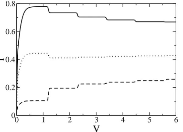
Fig. 2.3 shows the I(V ) characteristics for different α’s when cL is small, so that the polaron level lies closer to µR. In the experiment of Refs. [1, 5], this means that the nanotube has a large overlap with the conducting substrate. As long as M = 0, that is if V < Ω/cL (this condition is satisfied on the bias-voltage range which is plotted), P0
n ≈ δn0, which results in the PDC behavior of I(V ). The PDC steps correspond to N increasing by 1 each time V passes through a multiple integer of Ω/cR. Explicitly, the current-step amplitude at V = nΩ/cR corresponding to the current increase is given by
∆I(n)= ΓLe−α
2 α2n
n! . (2.12)
For smaller α’s the current-step amplitude decreases faster with increasing V , which leads to the saturation of the current at lower voltages. Note that the first step (low bias voltage) is rounded. This feature is specific to the fact that the capacitances are asymmetric: at small V , when the chemical potential of the lead with the largest capacitance remains close to the polaron level, thermally activated tunneling processes can be effective.
0 2 4 6 8 V 0 0.2 0.4 0.6 0.8 1 I
Figure 2.3: The case cL= 0.1 for α = 0.8 (solid), 1.5 (dashed) and 1.9 (dot-dashed). In all figures, the current I is plotted in units of ΓLΓR/(ΓL+ΓR), while the voltage V is given in units of Ω (we use e = ¯h = 1). We take T = 0.01 Ω, E = 0, and ΓL/ΓR= 10−4 unless noted otherwise.
Fig. 2.4 shows the I(V ) characteristics for the “reversed capacitance” case corresponding to a relatively large cL, when the polaron level is closer to µL. Within the plotted bias-voltage range, the current changes by steps when V passes through a multiple integer of Ω/cL, as before. At these points, M increases by 1; correspondingly, one more phonon-assisted channel is added. For α = 1.5 one still observes the PDC behavior, although the height of the current steps is strongly suppressed compared to the previous case on Fig. 2.3. For α < 1 NDC occurs in the first step, and with decreasing α, more NDC steps appear.
0 1 2 3 4 5 6 V 0 0.2 0.4 0.6 0.8 I
Figure 2.4: The case cL= 0.9 for α = 0.5 (solid), 0.9 (dotted) and 1.5 (dashed).
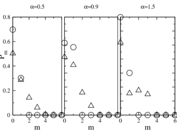
The phonon distributions P0
m, which play the role of probabilities of open channels, at different bias voltages are shown on Fig. 2.5. This figure demon-strates the increase of the number of phonon excitations (far out of equilibrium) with increasing M in Eq. (2.9). It shows that at given V , the phonon occupation number is restricted by M − 1.
0 2 4 m 0 0.2 0.4 0.6 0.8 Pm α=0.5 0 2 4 m α=0.9 0 2 4 6 m α=1.5
Figure 2.5: Phonon distribution, P0
m, for the case of Fig. 2.4 at the bias voltage V /Ω = 2 (circles) and 4 (triangles).
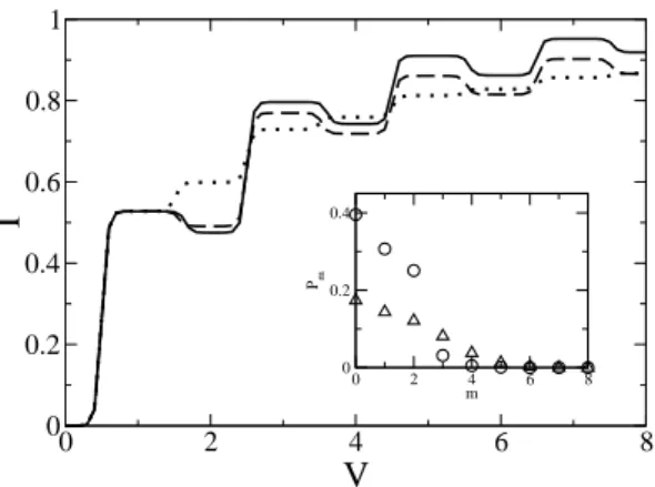
The possibility of NDC is not only restricted to the strongly asymmetric case cL ≫ cR, but it can also be present in the more general situation when cL and cR are comparable, see Fig. 2.6. Notice that in this more general case, I(V )
0 2 4 6 8 10 V 0 0.2 0.4 0.6 0.8 1 I
Figure 2.6: The case of cL= 0.4 for α = 1.9 (solid), 1.5 (dashed) and 0.8 (dot-dashed). characteristics exhibit steps of different length. In the shown case of cR = 1.5cL, the number N of phonon sidebands above the polaron level increases by 1 with the voltage period Ω/cR = (5/3) Ω; for these steps we always have a PDC behavior. At the same time, the number M of phonon sidebands below the polaron level increases by 1 with the voltage period Ω/cL = 2.5 Ω: one more channel becomes open which yields the possibility of NDC. The larger α, the more PDC-steps at low bias voltages are observed.
To demonstrate the role of asymmetry in the tunneling rates ΓL,R on current transport, in Fig. 2.7 we show I(V ) characteristics for the different cases of junction asymmetry. As is seen from the plots, the NDC steps in the cases of high and moderate asymmetry (ΓL/ΓR = 0.01 and 0.1, respectively) turn into PDC steps in the symmetric case (ΓL = ΓR). The height of the phonon-assisted steps in the asymmetric case is noticeably large compared to the symmetric one. This
0 2 4 6 8 V 0 0.2 0.4 0.6 0.8 1 I 0 2 4 6 8 m 0 0.2 0.4 Pm
Figure 2.7: For cL = 0.5, α = 0.8, T = 0.02 Ω, and E = 0.25 Ω: ΓL/ΓR = 10−2 (solid), 0.1 (dashed) and 1 (dotted). Inset shows the phonon distribution Pm0 at the bias voltage V = 4 Ω for ΓL/ΓR= 10−2 (circles) and 1 (triangles).
is related to the phonon distribution, an example of which (at V = 4Ω) is shown in the inset of Fig. 2.7. In the asymmetric junction, the number of phonons is restricted by M , while in the symmetric junction the phonon distribution is more spread out. As a result, in the symmetric case, the phonon-assisted contribution to the current is weakened.
Effect of the half–shuttle on I(V ) characteristics
We have also proposed that in a STM experiment, the tip-nanotube tunneling distance may deviate from its equilibrium value due to the “breathing” (radial) motion of the nanotube (see Fig. 2.1). Our model can easily be generalized to incorporate such an influence on the tip-nanotube coupling. Explicitly, we assume an exponential dependence of TL on the boson coordinate x = b + b†:
TL(x) = TL0e−sx , (2.13)
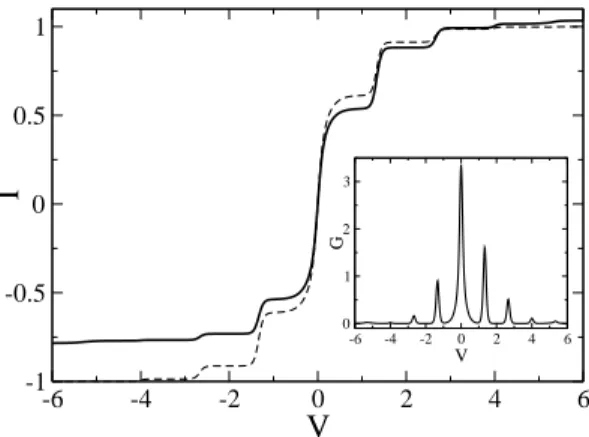
where s is determined by the ratio of the amplitude of the zero-point RBM oscillations to the electronic tunneling length (≈ 0.5 ˚A) which characterizes the tunnel barrier between the STM tip and the nanotube. Such position-dependent amplitudes are usually introduced in the context of nanomechanical electronic devices [6], where one refers to the “shuttle” mechanism as the central region oscillates between the two electrodes. In our case, we refer to the “half-shuttle” effect, because only one of the tunneling amplitude (left) is modified by the position.
The half-shuttle can be detected by the asymmetry of the current-voltage curves: the presence of half-shuttle mechanism (s 6= 0) violates the parity sym-metry of the current-voltage characteristics, leading to I(V ) 6= −I(−V ).
Approaching the STM tip closer to the nanotube should strongly enhance the half-shuttle mechanism. According to our estimation, the amplitude of the zero-point RBM oscillations is of the order of 1 pm, which corresponds to s ∼ 0.1. Fig.
-6 -4 -2 0 2 4 6 V -1 -0.5 0 0.5 1 I -6 -4 -2 0 2 4 6 V 0 1 2 3 G
Figure 2.8: Asymmetry of I(V ) due to “half-shuttle”: s = 0.1 (solid) and 0 (dashed). We take α = 0.7, cL = 0.25, E = 0, T = 0.04 Ω. The inset shows the differential conductance for s = 0.1.
2.8 shows I(V ) for the case when cLis relatively small, which is favorable for PDC. The current steps are suppressed at negative voltages (differential conductance peaks in the inset of Fig. 2.8), while at positive bias voltage, the current steps have a tendency to increase. In other words, the half-shuttle mechanism works in favor of the formation of the polaron state: the probability of phonon-assisted tunneling onto the dot from the left electrode is increased, while the phonon-assisted tunneling from the dot to the left electrode is decreased.
The case of relatively large cL is shown on Fig. 2.9. Like in the previous case, here we also observe suppression of the current steps at negative voltages. Numerically we have observed that when the poalron level is shifted, the
“half--6 -4 -2 0 2 4 6 V -0.5 0 0.5 I -6 -4 -2 0 2 4 6 V 0 1 2 3 G
Figure 2.9: Same as Fig. 2.8 but for cL= 0.75.
shuttle” mechanism tends to reinforce the NDC regions, but it cannot trigger this behavior on its own.
2.2 TRANSPORT IN THE POLARON CROSSOVER REGIME
There has been a large amount of theoretical work on the problem of tunneling through a resonant level coupled to a phonon mode. The approaches basically fall into two categories. The first category is the kinetic equation approach, which is relevant in the high temperature (or the weak tunneling) limit. Such an approach has been applied in Sec. 2.1. The second category deals with the opposite limit of low temperature (or the strong tunneling coupling). In this limit, the Landauer formulation of transport combined with the non-equilibrium Green function tech-nique serves as a good starting point for computing transport. Depending on the strength of the electron-phonon coupling, various approximation schemes have been developed for weak electron-phonon coupling [7] and for the intermediate to strong coupling, where the electrons of the molecular quantum dot are dressed by a polaron cloud [8, 9, 10, 11, 12, 13, 14]. In paper VIII we go beyond the existing polaron approaches to molecular transport, allowing a better description of the intermediate electron-phonon coupling regime.
Perturbation theory is typically formulated in terms of (single) phonon Green functions. Yet when electron-phonon interaction is not weak, a more natural choice is to introduce a Green function which describes collective phonon exci-tations associated with the polaron cloud. We show that the electron spectral function of the molecular quantum dot can be evaluated systematically by dia-gram dressing of the polaron Green functions. With increasing tunneling coupling to the leads, correlations between polaron clouds become more important sug-gesting that phonon features for the current through the molecule could be more pronounced than expected. In particular, we have found that polaron-cloud cor-relations lead to a strong sharpening of the peak structure in the spectral function of the molecule: at relatively high temperature the phonon sideband peaks are much narrower than the tunneling coupling would suggest.
Keldysh Green function approach in the polaron representation
We use the same model as in Sec. 2.1 to describe a molecular quantum dot with a single-electron level coupled to a local vibration mode of frequency Ω. The Hamiltonian of the molecule coupled via tunneling to two metallic leads is given by H = HM+ HT + Hleads [see Eq. (2.1)], where the Hamiltonian of the molecule reads (e = ¯h = 1): HM = h ǫ0− g ³ b + b†´id†d + Ω b†b . (2.14)
We ignore the spin degree of freedom assuming a resonant tunneling situation in the Coulomb blockade regime, far from the Kondo regime. The bias voltage V = µL− µRis imposed by shifting the chemical potentials (µj) of the leads, and we consider the symmetric junction with TL,R = T .
In the steady state, the current through the junction can be expressed in terms of the nonequilibrium Green functions of the molecule, and is given by the Meir–Wingreen formula [15]:
I(V ) = Γ
Z dω
8π [fL(ω) − fR(ω)] iA(ω) , (2.15) where fL,R(ω) are Fermi distributions in the leads, Γ is the tunneling width of the dot level, and A(ω) is the Fourier transform of the electron spectral function of the molecule,
A(t − t′) = −ih{d(t), d†(t′)}i , (2.16) which determines local electronic properties of the interacting region (molecule) in the presence of the leads.
As in Sec. 2.1, it is convenient to eliminate the electron-phonon coupling term in HM by using the polaron transformation (2.5). As a result, the transformed tunnel Hamiltonian becomes dressed by the vibrations,
˜ HT = X jk T∗ k c†jkD + h.c. , (2.17)
where D = dX and X = e−iαp is the polaron cloud operator. This form of ˜
HT suggests an effective phonon-mediated coupling between the dot and lead electrons.
We now introduce the Keldysh Green function for the polaron, G(t − t′) = −i h TC{ D(t)D†(t′)}i, where TC is the Keldysh time-ordering over the Keldysh contour C. Averaging over the leads yields:
G(t − t′) = −i h TC{S D(t)D†(t′)}i0, (2.18) where h ...i0 denotes averaging over the states of the molecule only, and the effec-tive S–matrix operator is given by
S = TCexp ½ −i Z Cdτ dτ ′D†(τ )Σ 0(τ − τ′)D(τ′) ¾ . (2.19)
The electron tunneling self-energy Σ0is built up from the Keldysh Green functions for the uncoupled leads, and can be expressed in terms of the tunneling coupling and electron distribution in the leads by virtue of Σ<,>0 (ω) = ±i (Γ/2)P
j fj(±ω). The main challenge for the perturbation theory in Σ0 resides in the fact that because the multi-phonon operator X accompanies the d operator in S, the Wick theorem is not applicable to express G in terms of the electron and phonon self-energies. It is nevertheless possible to develop a diagrammatic scheme and for-mulate the corresponding Feynman rules in the polaron representation. For this purpose, it is convenient to introduce a Keldysh Green function describing the polaron cloud:
Λ(t) = h TC ³
X(t)X†(t′)´i
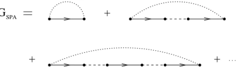
A typical approximation [16, 10, 12, 11], called the “single particle approximation” (SPA) in Ref. [13], consists in factorizing the electron Green function (2.18) as
G(t − t′) ≃ G(t − t′) Λ(t − t′) , (2.21) where G obeys the Dyson equation for the dot in the absence of phonons. Ac-cording to our analysis, this decoupling of electron and phonon dynamics can be justified in the anti-adiabatic regime [17], where Ω (and/or g) is large compared to Γ. The phonon mode is then fast and reacts instantaneously (on the time scale of Γ−1) to the presence/absence of an electron on the molecule. The Feynman
G
. . . SPA
Figure 2.10: Dyson series for G corresponding to the SPA, Eq. (2.21): Electron prop-agator G (solid lines), self-energies Σ0(dashed lines), phonon-cloud dressing propagator Λ (dotted lines).
diagrams associated with the SPA are depicted in Fig. 2.10. In each order the phonon cloud connects only the end points of the full fermionic lines.
Although the series expansion of G in the tunneling self-energy Σ0 (i.e., in Γ) is rather complicated in the presence of phonons, this expansion can be dras-tically simplified in the limit of Re Λ ≫ Im Λ. Neglecting Im Λ turns out to be a good approximation even for the case of an intermediate electron-phonon coupling, α < 1, and this result does not depend on temperature. Considering this case, we go beyond the anti-adiabatic regime and incorporate the effects of the polaron cloud in the vertex part of the Green function which are expected to become essential in the polaron crossover regime where Γ and Ω are compa-rable. Namely, in our treatment of the Dyson series for G, we take into account correlations between phonon clouds corresponding to two sequential tunneling events of the lead electrons, which are happening on the time scale of the order of Γ−1. In terms of the Feynman diagrams this is achieved by replicating the structure of the first order (in Γ) diagram: in all the higher orders, we keep only the nearest-neighbor crossing lines (representing Λ−1) which connect the dressed electron propagators and the dressed self-energies. The diagrams associated with our expansion scheme, which is labeled as the “nearest-neighbor crossing approx-imation” (NNCA), are illustrated in Fig. 2.11. By summing up all the terms of perturbation theory within the NNCA, we derive a set of Dyson-type equa-tions for the polaron Keldysh Green function, which is then used to calculate the spectral function of the molecule and/or the current.
G
. . . NNCA
Figure 2.11: Diagrammatic representation of the NNCA. As in Fig. 2.10, dotted lines above the fermionic line represent the phonon-cloud dressing propagator Λ, while dotted lines crossing below the fermionic line represent the undressing corrections described by Λ−1.
Calculation of the spectral function
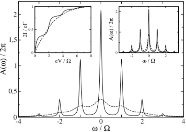
Although, the dressed by phonons self-energy becomes voltage-dependent, in-spection of this dependence shows that for α < 0.6 the magnitude of the lead self-energy Σ(ω) is only slightly decreased compared to the bare one. Thus, for moderate α’s the voltage dependence of the spectral function of the molecule can be discarded.
In Fig. 2.12 we plot the spectral function A(ω) = −2Im GR(ω) and the corre-sponding current calculated within the NNCA, and comparing with the SPA, for an intermediate coupling α = 0.4. In order to reveal the polaronic effects, it is ad-vantageous to assume that the leads have a lower temperature Tleads than that of the molecular quantum dot, T . In this situation, the leads act as a probe to detect the effect of vibrations on the electronic correlations on the molecule. When the molecule temperature is relatively high (T > Ω), several satellite peaks appear in the spectral function (see Fig. 2.12) associated with emission/absorbtion of vi-brational quanta. Although for small Γ, as expected, the NNCA and SPA results
-4 -2 0 2 4 ω / Ω 0 0,5 1 1,5 2 A( ω) / 2π -2 ω / Ω0 2 0 1 2 A( ω) / 2π 0 2 4 6 8 eV / Ω 0 0,5 1 2I / e Γ
Figure 2.12: A(ω) at T /Ω = 4 calculated within the NNCA (solid line) and SPA (dashed line), for α = 0.4, Γ/Ω = 0.8, and ǫ = 0. Left inset: I(V ) characteristics for Tleads/Ω = 0.1. Right inset: same as the main figure but for 2Γ/Ω = 0.2.
seen for the higher transparency (the main plot of Fig. 2.12). In this case, the current in the NNCA undergoes sharp steps corresponding to the phonon side-bands, while the current in the SPA does not show any structure (see left inset of Fig. 2.12). According to the NNCA, all excited satellite peaks remain sharp and are rather robust with respect to increasing Γ. This is the regime where the SPA breaks down. In this transition region, increasing the temperature acts in favor of the electron-phonon interaction which tends to localize the dot electron, leading to a well pronounced peak structure in the spectral function. This retardation effect is captured by taking into account correlations between phonon clouds in the NNCA. With increasing Γ > Ω, we expect that the NNCA becomes less suf-ficient, and the higher order correlations between the polaron clouds should also be included.
The effect of suppression of the tunnel broadening in the spectral function at high temperature could be observed directly in the measurement of the differential conductance keeping the leads at very low temperature (Tleads ≪ Ω), so that dI/dV ∝ A(eV ), but varying the local temperature of the molecule. For artificial molecules such as µm-sized carbon nanotubes, this could be achieved by local heating with a laser (with a spot size around 100 nm or less). The intermediate coupling regime has been realized in a recent experiment where the vibration corresponds to a stretching mode of the nanotube [3]. Laser heating may not be realistic for a true molecule because of the reduced size of the junction, but in the latter case it is reasonable to assume that molecule heating will still occur because of current flow (granted, these heating effects are not controlled, and are not described in the present model) implying some enhancement of phonon features in transport through the junction.
SUPERCONDUCTING TRANSPORT THROUGH A
VIBRATING MOLECULE
Molecular electronics is particularly exciting because of the possibility to contact molecules by leads of different nature. In this chapter, we discuss how electron transport is affected by a coherent phonon mode coupled to the molecular charge for the case of (s-wave) superconducting leads. Molecules connected to supercon-ductors promise a rich terrain of exploration that allows for new spectroscopic tools (probing molecular properties), potentially useful applications, and inter-esting fundamental physics. First experimental results have already appeared for carbon nanotubes [18, 19, 20, 21] and metallofullerens [22].
3.1 INELASTIC MULTIPLE ANDREEV REFLECTION WITH PHONONS
So far transport through molecules has been theoretically studied only for normal leads, either using rate equations in the high-temperature regime, or perturba-tion theory in the electron-phonon coupling [7] in the quantum-coherent regime. While the combination of the vibrational coupling and correlation transport has barely been investigated in the context of supercurrent [23]. As it is well known for superconducting leads and large transmission through the junction, subgap transport is ruled by Multiple Andreev Reflection (MAR) processes [24]. These have been extensively studied for point contacts [25, 26, 27] and for junctions containing a resonant level [28, 29]. In paper IV, we provide a theoretical frame-work to include vibrations into superconducting transport through a resonant molecular level, and for the first time we establish a connection between the Keldysh formalism and the Landauer scattering approach for inelastic MAR. In the paper, we focus on the most interesting quantum-coherent low temperature limit with high transmission, where Coulomb charging effects are largely wiped out, and therefore can be neglected. We compute the dc current basically for the entire bias voltage range within a Keldysh Green function scheme valid for small electron-phonon coupling (g) but arbitrary phonon frequency (Ω).
Model and Keldysh approach
We choose a tractable model describing the relevant physics of a molecule sand-wiched between two superconducting leads. The model Hamiltonian is given by (we put e = ¯h = 1 in intermediate steps)
H = Ωb†b +X σ
(ǫ0− gx)d†σdσ+ HL+ HR+ HT , (3.1) where we consider one relevant (resonant) molecular level associated with the fermion operator dσ for spin σ =↑, ↓ and located at the energy ǫ0. In Eq. (3.1) we take a linear coupling between the molecular charge and the phonon displacement x = b + b†. The leads (j = L, R) are described by a pair of standard s-wave BCS Hamiltonians, and the lead-molecule coupling is
HT =
X k,j=L/R=±
ψjk† T σze±iσzV t/2d + h.c. , (3.2) where the bias voltage V enters via the time-dependent phase difference. Here we use Nambu spinor notations for electronic degrees of freedom,
ψjk = Ã ψjk,↑ ψ†j,−k,↓ ! , d = Ã d↑ d†↓ ! , (3.3)
and σz is a standard Pauli matrix in Nambu space.
Because the calculation of MAR-dominated transport is already involved in the absence of phonons (g = 0), a nontrivial current-conserving self-consistent approach covering the large transmission limit seems out of question. The self-consistency is usually sufficient to ensure current conservation. However, we instead use a perturbation theory with the small expansion parameter g/Γ, where Γ is the tunneling half-width, assuming the electron-hole symmetric case, i.e., ǫ0 = 0, ΓL,R = Γ, and ∆L,R = ∆ (with ∆ the superconducting gap), where current conservation is known to hold [30].
To compute the current-voltage characteristics, we employ the Keldysh Green function technique and calculate the Keldysh Green function for the d fermion,
Gσσ′(t, t′) = −ihTC[dσ(t)d†σ′(t′)]i, (3.4)
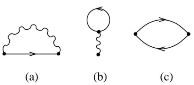
where TC is the time-ordering operator along the Keldysh contour. Similarly, we define a phonon Keldysh Green function D(t, t′) for the phonon variable x = b+b†. Denoting the respective functions for g = 0 by G0 and D0, and using the self-energy diagrams in Fig. 3.1, the dressed Green functions used in our perturbative approximation follow from the Dyson equations:
G−1 = G−1
0 − Σph , (3.5)
(a)
(b)
(c)
Figure 3.1: Self energy due to the presence of the phonon mode: (a) “Fock” and (b) “tadpole” diagram. The polarization bubble (c) leads to the dressed phonon propagator
ˇ
D (wiggly lines). Arrowed lines denote ˇG0.
For numerical analysis, it is convenient to use the double Fourier representation
G(t, t′) = +∞X n,m=−∞ Z F dω 2π e −iωnt+iωmt′ Gnm(ω) , (3.7)
and likewise for all other Green functions and self energies. Here ωn = ω + nV (n integer) for ω within the fundamental domain F ≡ [−V/2, V/2]. For fixed ω ∈ F , the Dyson equations then take the form of matrix equations in the Fourier representation.
The dc current through the left/right junction is given by
IL/R = ∓ Re X nm Z F dω 2π tr h σzΣL/R,nm(ω) Gmn(ω) i+− , (3.8)
where Σj is the electron self energy due to tunneling coupling to lead j, and the trace “tr” extends over Nambu space. Eq. (3.8) constitutes a generalization of the Meir-Wingreen formula [15] to the case of superconducting leads.
In paper IV, we establish a close connection between the above Keldysh Green function approach and a Landauer scattering approach incorporating in-elastictransitions. Such an approach is formulated using the equation-of-motion method, where transfer matrices matching electron/hole scattering states in the presence of phonons are expressed in terms of Keldysh Green functions. The de-veloped “inelastic MAR” picture is in fact essential in interpreting our numerical results.
Subgap regime: Inelastic MAR
Using Eq. (3.8), we have evaluated the I-V characteristics for g = 0.15Γ and kBT /∆ = 0.01. Besides the current, we have also monitored the average phonon number Nph = hb†bi, which has always been less than 1, in accordance with our assumption of weak electron-phonon coupling.
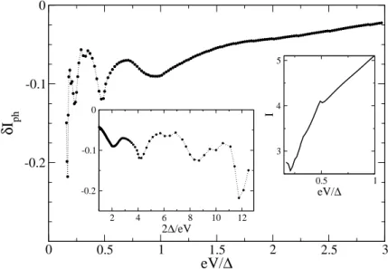
We start with the subgap regime, where MAR provides the dominant trans-port mechanism. For 2∆/(n + 1) < eV < 2∆/n (n integer), there is a total
number n of Andreev reflections for electrons (or holes) within the superconduct-ing gap: an electron/hole is alternately retroreflected at the junction interfaces as a hole/electron, and each time a Cooper pair is passing through the junction. The I-V curve for Γ = 2∆ and Ω = 0.2∆ is given in Fig. 3.2, where the phonon contribution to the current δIph ≡ I(g) − I(g = 0) is always negative. In this fully transmitting limit, the I-V curve for g = 0 is smooth and does not exhibit the MAR cusps encountered at lower transmission [25]. However, phonons restore such features near MAR onsets, with pronounced even-odd parity effects: For even (odd) n, δIph shows valleys (peaks) around eV = 2∆/n. This is clearly seen in the left inset of Fig. 3.2 for n up to 12. The appearance of even-odd parity oscillations is quite distinct and surprisingly regular given the complexity of this system. 0 0.5 1 1.5 2 2.5 3 eV/∆ -0.2 -0.1 0 δ I ph 0.5 1 eV/∆ 3 4 5 I 2 4 6 8 10 12 2∆/eV -0.2 -0.1 0
Figure 3.2: Phonon difference current δIph ≡ I(g) − I(g = 0) for ¯hΩ = 0.2∆ and Γ = 2∆. In all figures, currents are given in units of e∆/(2π¯h), and dotted lines are guides to the eye only. Left inset: Same as function of 2∆/eV . Right inset: Part of the total I-V curve (note the scales).
In order to achieve a physical understanding of this even-odd effect, it is useful to invoke a MAR ladder picture in energy space, including inelastic transitions caused by phonon emission. A schematic description of the MAR ladder picture is given in Fig. 3.3: the two superconductors are positioned at the same chemical potential, but electrons (from left to right) and holes (from right to left) “climb” the MAR ladder by gaining eV for each Andreev reflection. The higher the total number of Andreev reflections in one cycle, the larger the total charge transmitted. Since we consider the high transmission limit where high-order MAR processes are not penalized, the current is therefore expected to increase (decrease) if phonon emission is able to increase (decrease) the number of Andreev reflections in a MAR cycle. For eV slightly below 2∆/n with even n, we then
Ω Ω ∆ −∆ E E + 3 eV
Figure 3.3: MAR ladder picture with phonon emission. Here eV is slightly below ∆: for an electron incoming from the left side, we have one hole (open circle) and two electron (filled circle) segments. Dashed lines indicate possible trajectories after single phonon emission involving either hole or electron segments. There is also a MAR path (not shown) for a hole entering from the right side, with one electron and two hole segments.
argue as follows (for n = 2, see Fig. 3.3). For small energy transfer ¯hΩ, if a phonon is emitted during an electron segment, MAR trajectories in energy space are not drastically modified in the sense that the number of Andreev reflections stays unaffected. However, if a phonon transition occurs during a hole segment, the MAR ladder is shifted upwards by ¯hΩ and the last hole on the MAR ladder can be scattered into the continuum (left electrode in Fig. 3.3) instead of being Andreev reflected. Consequently, one Andreev reflection is lost and hence the current is expected to decrease. This argument applies both to incoming electrons and holes, and explains why current valleys are observed for eV ≈ 2∆/n with even n in Fig. 3.2. On the other hand, consider eV slightly above 2∆/n with odd n. Reiterating the above analysis, now phonon emission during a hole segment tends not to affect the number of Andreev reflections. If the phonon is emitted during an electron segment, however, an additional Andreev reflection has to take place to complete the MAR cycle, leading to a current peak for eV ≈ 2∆/n with odd n.
The I-V curve in the case of a high-frequency phonon mode, ¯hΩ = 1.8∆, is shown in Fig. 3.4. Now δIph can be positive and again shows oscillations near the MAR onsets, which are less pronounced (cf. Fig. 3.2) for small n = 2∆/eV . Remarkably, even for small voltages, eV ≪ ¯hΩ, a rather complicated subgap structure is caused by the phonon. At such low voltages, this is only possible via MAR, for otherwise electrons or holes do not have enough energy to emit a phonon. The broad minimum corresponding to n = 2 observed in Fig. 3.2 has now vanished: for eV < ∆, by emitting a high-energy phonon (¯hΩ > ∆), the last
0 0.5 1 1.5 2 2.5 3 eV/∆ -0.15 -0.1 -0.05 0 0.05 0.1 δ I ph 0.2 0.4 0.6 0.8 1 eV/∆ 3 4 5 I 2 4 6 8 10 12 2∆/eV -0.1 0 0.1 δ Iph
Figure 3.4: Same as Fig. 3.2 but for ¯hΩ = 1.8∆. The upper inset gives δIph as a function of 2∆/eV , the lower inset gives the low-voltage part of the total current.
electron on the MAR ladder can now be scattered back inside the gap instead of heading to the continuum. This increases the number of reflections and thus the current. As a phonon emitted during the hole segment has the opposite effect, the net outcome of the higher phonon frequency is to suppress the valley at eV ≈ ∆ expected for small Ω. Figure 3.4 also shows a dip in the current at eV ≈ 1.8∆, representing a phonon backscattering feature at eV = ¯hΩ.
Excess and Josephson current
We have also computed the difference δIexc,ph between the excess currents Iexc with and without the phonon. For the case of high transmission encountered here, we have found that phonons generally enhance the excess current. To give a concrete example, for ¯hΩ = 0.8∆, Γ = 2∆ and g = 0.5∆, we find δIexc,ph/Iexc≈ 0.07. A similar current enhancement at high transmission was also found for environmental Coulomb blockade in superconducting junctions, and has been explained as “antiblockade” effect [31]. As such, this effect of the phonon mode may not be too surprising.
By adopting our approach to the Matsubara representation, we have also cal-culated the equilibrium Josephson current flowing through the vibrating molecule. For arbitrary parameters, it is straightforward to numerically compute the full current-phase relation I(φ). However, in the adiabatic phonon regime defined by
¯hΩ ≪ ∆ ≪ Γ , (3.9)
that the Josephson current is given by
I(φ) = (e∆2/2¯h) D sin(φ)/Ea(φ) , (3.10) where
Ea(φ) = ∆[1 − D sin2(φ/2)]1/2 (3.11) is an Andreev bound state energy in the junction with an effective transparency
D = 1
1 + (g/2Γ)2. (3.12)
The φ-dependent shift without any broadening of the Andreev level caused by the coupling to a phonon mode is characteristic for the coherent limit and decreases the critical current. Very similar results were reported in Ref. [23], where the opposite limit Γ ≪ ∆ has been studied by lowest-order perturbation theory in the molecule-lead hopping.
3.2 PHONON SQUEEZING BY JOSEPHSON CURRENT
Nanoelectromechanical (NEM) systems have been a subject of extensive research in recent years. The possibility of combining electrical and mechanical degrees of freedom on the nanoscale may give rise to technological advances as well as manifestations of fundamental physical phenomena. In particular, a challenging goal consists in creating non-classical vibrational states, similar to non-classical states of light, with reduced quantum fluctuations in one of the mode quadra-tures, the so-called squeezed states. Besides the fundamental interest, this would also allow to exploit the quantum properties of mechanical degrees of freedom for applications in areas such as weak force detection, precision measurement, and quantum information processing. The generation of squeezed states in bulk materials was proposed in [32, 17, 33]. Recently, different squeezing scenarios have been suggested for nanomechanical resonators driven by nonlinear couplings [34, 35, 36, 37].
The excitation of molecular vibrations by an electronic current has been ob-served with normal metallic leads in several molecules including fullerenes and carbon nanotubes [38, 39]. The latter are in fact NEM systems, where charge fluctuations are coupled to bending [40], stretching [3] or radial breathing modes (RBM) [1]. Incoherent polaronlike charge fluctuations due to transport trigger a nonequilibrium distribution of the phonon mode. In paper V, we address the superconducting regime, and show that, for transparent lead-molecule contacts, the Josephson effect survives a strong electron-phonon interaction and triggers co-herent phonon fluctuations. As a striking consequence, the conjugate momentum of the molecular distortion displays reduced zero-point fluctuations (squeezing), including nearly Gaussian minimum-uncertainty states. The magnitude of the phonon squeezing can be controlled by varying the superconducting phase differ-ence, and is also sensitive to the junction asymmetry.
Squeezed states
The concepts of coherent and squeezed states were both elaborated mainly in the context of quantum optics. A coherent state is a phase-coherent sum of (photon) number states. In this state, the quantum fluctuations in any pair of conjugate variables are at the lower limit of the Heisenberg uncertainty principle. In other words, a coherent state is as “quiet” as the vacuum state. Squeezed states are interesting because they can have smaller quantum noise than the vacuum state in one of the conjugate variables (quadratures).
For a harmonic oscillator described by the Hamiltonian Hosc= Ωb†b, a general class of Gaussian minimum-uncertainty squeezed states is defined as follows [41]:
|λ, ηi = D(λ)S(η)|0i , (3.13)
where D(λ) = exp³λb†− λ∗b´ is a displacement operator, and S(η) = exph(η∗/2)b2
− (η/2)b†2i
(3.14)
denotes the squeezing operator. The state |λ = 0, ηi is referred as the squeezed vacuum state, and the absolute value of η = ρ eiθ/2 is called the squeezing pa-rameter. For vacuum squeezed states, the quadrature components x1,2, defined by b = eiθ/2(x
1+ ix2) /2, fulfill the uncertainty relation δx1δx2 ≥ 1, where the variance of one component, δx1 = e−r is reduced below the standard quantum limit of 1, whereas the noise in the other component is enhanced, δx1 = er. Be-cause of these properties, squeezed states form an exciting group of states that can provide unique insight into quantum mechanical fluctuations.
A familiar method in quantum optics to generate a squeezed state of a har-monic oscillator is to use a parametrically driven nonlinear potential correspond-ing to the Hamiltonian
Hosc,p(t) = Ω b†b + ζ(t)b†2+ ζ∗(t)b2. (3.15) For NEM systems, the application of this method has been proposed in [34], but the requirements, a sufficiently strong nonlinearity to overcome the losses, and preparation of an initial state close to the ground state of harmonic oscillator, are not easily to met.
Another method of introducing nonlinear terms to produce squeezing is to couple a harmonic oscillator to a two-level system. Such a scenario but in the context of “engineering” dissipation has been suggested in [35] by coupling a nanoresonator to a Cooper pair box (the latter plays the role of a dissipative two-level system). In paper V, we suggest an alternative scenario to generate squeezing by employing a true microscopic two-level system: coherent nonlinear effects in a molecular conductor are realized due to the interaction between the phonon mode and a pair of Andreev (subgap) states formed in the junction region by the gradient of the superconducting phase.