HAL Id: tel-00185371
https://tel.archives-ouvertes.fr/tel-00185371
Submitted on 5 Nov 2007
HAL is a multi-disciplinary open access archive for the deposit and dissemination of sci-entific research documents, whether they are pub-lished or not. The documents may come from teaching and research institutions in France or
L’archive ouverte pluridisciplinaire HAL, est destinée au dépôt et à la diffusion de documents scientifiques de niveau recherche, publiés ou non, émanant des établissements d’enseignement et de recherche français ou étrangers, des laboratoires
QUASIPARTICLES IN A DIFFUSIVE CONDUCTOR:
INTERACTION AND PAIRING
S. Gueron
To cite this version:
S. Gueron. QUASIPARTICLES IN A DIFFUSIVE CONDUCTOR: INTERACTION AND PAIRING. Condensed Matter [cond-mat]. Université Pierre et Marie Curie - Paris VI, 1997. English. �tel-00185371�
Quasiparticles in a diffusive conductor:
Interaction and pairing
Sophie Gueron
Quantronics Group
THESE DE DOCTORAT DE L'UNIVERSITE PARIS 6
Quasiparticules dans un conducteur diffusif :
interactions et appariement
specialite :
Physique des solides
Presentee par :
Sophie
Gueron
pour obtenir le grade de docteur de l'Universite Paris 6
Soutenue le 17 octobre 1997
Amphitheatre Claude Bloch,
Orme des merisiers,
CEA-Saclay.
devant le jury compose de
President:
J. Bok
Rapporteurs:
T. Klapwijk
B. Pannetier
Examinateurs :
H. Bouchiat
M. Devoret
G. Montambaux
A mes grand-parents
Genevieve Bernheim, Jules Gueron, Anna Kostokovsky, Louis Tabachnick, A mes parents,
A Claire, A Benoit.
Errors in some formulas of Chapter 5 in the first edition of this thesis were pointed out to us by John Martinis. The definition of Hoon p. 101, formulas (5.52) to (5.54), formula (5.59), formulas (5.61) to (5.67), and the corresponding formulas on pages 141 and 142, have been edited and corrected in this second edition.
Hugues Pothier and Sophie Gueron, Saclay, December 1998
Remerciements
Mes remerciements s'adressent tout d'abord au Groupe de quantronique, au sein duquel j'ai effectue ce travail. Faire partie du groupe a signifie pour moi etre contaminee par la conviction que tous les phenomenes peuvent etre compris en termes intuitifs, et decrits par une image qui, si elle est correcte, doit pouvoir etre illustree par une experience simple et claire. L'idee d'une experience nee d'heures de discussions au tableau d'une salle informatique exigue illustre Ie petit miracle qui s' accomplit lorsque s' allient curiosite, reflexion, ecoute, creativite et enthousiasme. Au sein du groupe, j'ai eu l'impression de grandir en meme temps que progressaient les experiences et leur comprehension.
Je remercie Michel Devoret, mon directeur de these, pour l'attention constante qu'il m'a prodiguee, Ie soin avec lequel il ma explique les concepts qu'il jugeait fondamental de comprendre, au cours de nombreuses discussions dans lesquelles j 'admirais la combinaison de la rigueur de raisonnement et de la presentation claire des concepts. Daniel Esteve, en directeur de these dual, m'a enseigne aussi bien les techniques experimentales, nanometriques et macroscopiques, que la facon de considerer une theorie de plusieurs points de vue differents. Son dynamisme et son efficacite epoustouflants rendent sa gentillesse et l'importance qu'il apporte aux relations personnelles d'autant plus emouvantes, Hugues Pothier complete Ie trio: aucune des experiences presentees dans cette these n'aurait pu etre realisee sans lui. Ses idees astucieuses ont permis la fabrication d' echantillons complexes, et son irreverence a grandement contribue
a
desacraliser les theories, etape essentielle dans la comprehension de concepts qui me sont ensuite devenus familiers. Ses encouragements, moqueries bienveillantes, jeux de mots toujours subtils lors de son suivi permanent de mon travail, ont fait de cette these un bonheur quotidien. Je remercie tous trois de l'aide extreme et permanente qu'ils m'ont apportee durant la redaction du manuscrit.J'ai eu grand plaisir
a
travailler avec Norman Birge durant sa visite au laboratoire, durant laquelle ont ete realisees les experiences sur la mesure de la densite d'etats et l'interaction entre quasiparticules. II m'a fait partager ses connaissances, m'initiant aux charmes de la detection synchrone Lock-in,a
la rigueur experimentale en general, sans parler de la tarte au potiron. C' est dans ces conditions de travail exceptionnelles, qui ont pu rappelera
certains Ie BTP chilien, que j' ai decouvert la richesse des experiences sur les systemes alliant nature quanti que et classique.Je remercie Cristian Urbina, pour l'aide qu'il m'a apportee, pour les mesures experimentales, pour la comprehension theorique, ainsi que lors des preparations d'exposes, durant lesquelles j'ai cherche a m'inspirer de ses qualites de pedagogue. Je lui suis egalement reconnaissante d'avoir organise des cours de mecanique, et accorde une profonde importance au fait d'avoir pu, avec Elke Scheer, beneficier du premier cours.
Admirative de la competence technique de Pief Orfila, de I'ingeniosite avec laquelle il demontre et demonte les mecanismes, je lui suis reconnaissante d'avoir consenti a parfois faire de moi son apprentie. Merci a Denis Vion pour son dynamisme extraordinaire, son extreme gentillesse, et l'enthousiasme qu'il montre pour toutes choses, en particulier pour mes experiences! Merci a Philippe Joyez pour ses conseils dans la fabrication des cables coaxiaux, son aide pour I'interpretation de I'experience sur le role de l'environnement dans la conductance tunnel. Son soutien grandissant, sa gentillesse durant la redaction de la these m'ont touchee. J'ai apprecie la complicite avec Vincent Bouchiat pendant notre travail de these dans le groupe. Je le remercie de ses conseils avises pour la fabrication des echantillons, son aide inestimable a la composition de cet ouvrage, notamment en ce qui concerne les micrographies, et la manipulation hasardeuse des logiciels.
Merci a Jan van Ruitenbeek de l'interet qu'il a porte a mon travaillorsqu'il etait en visite dans le Groupe. Merci a Elke Scheer pour sa gentillesse, ses conseils, son amitie, et l'exemple qu'elle constitue pour moi.
Merci a Philippe Lafarge qui m'a incitee a debuter rna these dans le Groupe, tout comme Georges Lampel et Yves Quere, dont les conseils m'ont conduite ici, notamment celui concernant le coup de foudre dans le choix du laboratoire de these.J'envie a Frederic Pierre la chance qu'il a de tout juste commencer sa these!
En outre, j'ai eu le plaisir de pouvoir discuter durant le cours de rna these avec Wolfgang Belzig, Helene Bouchiat, Christoph Bruder, Herve Courtois, Hermann Grabert, Gerd Ingold, John Martinis, Gilles Montambaux, Yuli Nazarov, Bertrand Reulet et Bernadette Sas. Merci aussi a Julien Bobroff pour son soutien et nos echanges d'impressions.
Merci egalement ames professeurs de mecanique Michel Juignet et Vincent Padilla, Patrice Jacques et Jean-Michel Richomme.
Je remercie Teun Klapwijk et Bernard Pannetier d'avoir bien voulu etre rapporteurs de rna these, et Julien Bok, Helene Bouchiat, et Gilles Montambaux d'avoir accepte de faire partie
Je suis reconnaissante
a
Daniel Beysens et Tito Williams de m'avoir accueillie dans le Service de Physique de l'Etat Condense et de m'avoir permis de beneficier d'un contrat CEA, ainsi qu'a Jacques Hamman et Louis Laurent de leur interet pour mon travail et le deroulement de rna these. Je suis tres reconnaissantea
Mme Marciano de sa gentillesse extreme, admirative de son efficacite directe et de sa capacitea
ne pas s'effarer de mes balourdises dans les demarches officielles.Enfin, merci
a
Christine, Colin, Pauline, Cecile, Anais, Jules, Charlie, Katrin, Maria, Odile, Vicky, Diego, Thomas, Isabelle, Remi, Cecile, Elinore, Julian, Marie-Helene, Olivier, Anne, Dominique, Jerome, Emmanuel, et Hans Georg, pour le soutien et le reconfort que m'a apportes leur gentillesse.Dans un mois, dans un an, comment souffrirons- nous, Seigneur, que tant de mers me separent de vous? Que le jour recommence et que le jour finisse Sans que jamais Titus puisse voir Berenice?
Table of Contents
1 Introduction 11
1.1 Quasiparticles in a disordered metal . . . .. 11 1.2 Interaction between quasiparticles in a diffusive wire 12 1.3 Density of states in a normal metal in contact with a superconductor. . . .. 16
1.4 Coherent transport at an NS boundary: the NS-QUID 19
REFERENCES 22
2 Experimental techniques 23
2.1 Sample fabrication . . . .. 23
2.1.1 Wafer preparation 24
2.1.2 Processing of a single chip 26
2.1.3 Examples: two particular samples fabricated with the trilayer process 29
2.2 Sample measurement at low temperature 36
REFERENCES 38
3 Observation of energy redistribution between quasiparticles in mesoscopic wires 39 3.1 Can the interaction between quasiparticles be probed? 39 3.2 Energy distribution function of quasiparticles in a mesoscopic diffusive wire 41 3.2.1 No quasiparticle scattering, no phonon scattering 41
3.2.2 Strong interaction between quasiparticles 42
3.2.3 Limit of strong interaction between quasiparticles and phonons 43 3.2.4 Relevant mechanisms in copper wires at low energy and temperature 45 3.3 Measurement of the energy distribution function in metallic wires (article) 46
3.4 Experimental procedures and controls 61
3.4.1 Test of the tunnel probe 61
3.4.2 From the tunnel probe differential conductance to the energy distribution function 63 3.4.3 Influence of the reservoir temperature on the scaling property 67 3.5 Interpretation of the data within the quantum Boltzmann equation 72 3.5.1 Interaction kernel inferred from the scaling property of the data 72 3.5.2 Numerical implementation of the quantum Boltzmann equation , 72 3.5.3 What does the experiment imply for the interaction kernel? 75
3.6 Conclusion 77
REFERENCES 79
4 Theory of electron-electron interaction in diffusive metals 81
4.1 Predictions of the theory of diffusive metals 81
4.1.1 Derivation of the kernel of the quasiparticle-quasiparticle interaction in the simple case of a potential V (r - rl
) • • • • • • • • • • . • • • • • • • . • • • • • • • • • • • • • • • • • • • • • • • • . • • • • • • • • • • • • • • • • • . • • • . . . • • • • 81 4.1.2 Interaction potential in infinite diffusive metals 86 4.1.3 Prediction for the kernel function . . . .. 86
4.1.4 Extension to finite systems 86
4.1.5 One-dimensional wire connected to reservoirs 87
4.1.6 Can this theory explain the experimental results? 87 4.1.7 Could a modified theory explain the experimental results? 88 4.2 Phenomenological model leading to the experimentally observed interaction kernel 89
4.2.1 Fluctuations of the current in a resistor 89
source " 90 4.2.3 Rate of the transitions induced in a resistor by the current fluctuations in another 92 4.2.4 Kernel of the effective quasiparticle-quasiparticle interaction 92 4.3 Towards a fully quantum microscopic theory. . . .. 94 REFERENCES. . . .. 95
5 Theoretical description of the proximity effect ., 97
5.1 Definitions of the Green functions used in the description of the proximity effect 100
5.1.1 The impurity averaged Green function 100
~5.1.2 The global Green function 101
5.2 Equilibrium proximity effect 103
5.2.1 Parametrization of Green functions by angles on the complex unit sphere 103 5.2.2 Physical properties in terms of the pairing angle () 106
5.2.3 The equilibrium Usadel equations 107
5.2.4 Example of a solution to the Usadel equation: disordered BCS Superconductor 109
5.3 Boundary conditions for the Green functions 113
5.3.1 Reservoirs 113
5.3.2 Spectral current conservation at an interface 113
5.4 Application to simple cases. . . .. 115
5.4.1 NS bilayers 115
5.4.2 Semi-infinite normal wire connected to a superconducting one 120
5.5 A variational principle for the Usadel equations 128
5.5.1 The effective potentialU 128
5.5.2 Pairing angle in a normal wire of finite length between a superconducting and a normal
reservoir 129
5.5.3 Wires and tunnel junctions as springs on the unit sphere 130
5.5.4 Example: the NS-QUID 131
5.6 Non-equilibrium proximity effect 134
5.6.1 Equation for the Keldysh Green function
K
and expression for the current 134 5.6.2 Equation for the filling functionf . . . .. 134 5.6.3 Current expressed in terms of pairing angle and filling functions 136 5.6.4 Zero voltage conductance of NS structures at zero temperature. . . .. 137 5.6.5 Examples. . . .. 1385.7 Tables of expressions contained in this chapter 141
REFERENCES 143
6 Measurement of the density of states in the presence of proximity effect 145
6.1 Introduction 145
6.2 Measurement of the density of states in a normal wire in good contact with a
superconductor (article) 146
6.3 Density of states in a perpendicular magnetic field 151 6.4 Contribution of charging effects to the measured DOS 154 6.4.1 What is measured by the differential conductance? 154
6.4.2 Form ofP(E,T = 0) for an RC environment 155
6.4.3 Control experiment on the contribution of charging effects 156 6.5 Effect of a finite temperature on the measurements. . . .. 162 6.6 Influence of the deposition order of the normal and superconducting metals 163
7 Simplified theory of the proximity effect in the limit of small pair correlations 167
7.1 Weak proximity effect 169
7.1.1 Green functions in the perturbative limit " 169 7.1.2 Pairing parameters in the weak proximity effect in the one-dimensional case 169 7.1.3 Expression for the current at an NS tunnel junction. . . .. 170 7.1.4 Linearized Usadel equations in a normal wire with planar junctions to
superconduc-tors 172
7.2 Solution of the linearized Usadel equation in terms of classical diffusion propagators . . . .. 174
7.2.1 Solution of the linearized Usadel equation 174
7.2.2 Link to the classical diffusion probability 174
7.2.3 Current at an NIS tunnel junction " 176
7.3 Direct calculation of the Andreev current using second order perturbation 177 7.3.1 Andreev reflection as a two quasiparticle tunnelling process " 177 7.3.2 Calculation of the two quasiparticle tunneling rate 179 7.4 The NS-QUID: modulation of the Andreev current . . . .. 183
7.4.1 Description of the NS-QUID 183
7.4.2 Field-dependent contribution to the current. . . .. 184
7.5 Why spin-orbit scattering has no effect 186
7.6 Conclusion 187
REFERENCES 188
8 Experimental investigation of NS-QUIDs 189
8.1 First experimental demonstration of the current modulation in an NS-QUID (article) 190
8.2 Three NS-QUIDs fabricated simultaneously 195
8.2.1 Characteristics of the measured samples 195
8.2.2 Measured modulated current in the two samples and comparison with theory. . . .. 198
8.2.3 Non-modulated current 199
8.3 Conclusion 201
8.3.1 Comparison with the DC-SQUID 201
8.3.2 The ultimate NS-QUID 202
REFERENCES 203
9 Present understanding of the proximity effect 205
9.1 Equilibrium proximity effect 206
9.1.1 Modification of the density of states. . . .. 206
9.1.2 Supercurrent , 206
9.2 Non-equilibrium proximity effect 208
9.2.1 Resistance of normal wires 208
9.2.2 Resistance of tunnel junctions 211
9.2.3 Arbitrary NS structures 212
REFERENCES 213
10 Conclusion 215
10.1 What ultimately limits the coherence of mesoscopic samples? 215
10.2 Open questions about the proximity effect 215
A Scattering approach to conductivity: from N to NS circuits A.I Expression of the conductance in the scattering formalism
A.I.l Landauer formula for the normal state conductance of a scatterer A.I.2 Andreev conductance of an NS system
A.2 Distribution of transmissions of complex circuits
A.2.I Generating function for the transmission distribution A.2.2 Transmission distributions of simple elements A.2.3 Combination rules and examples
A.2.4 From the transmission distribution to Andreev conductance REFERENCES 219 220 220 222 223 223 223 223 226 227 List of references ... 229 Index 235
Chapter 1
Introduction
1.1
Quasiparticles in a disordered metal
Although electrons in a metal constitute a many-body system of particles interacting strongly through the Coulomb repulsion, the independent electron model, pioneered by Drude and Sommerfeld, has proven very successful in explaining practically all properties of met-als. The theoretical justification of this simplification is due to Landau, who showed that any system of interacting fermions maps onto a system of independent fermionic particles, the "quasiparticles", which are the real particles with their quantum correlations [1]. Inmetals, a quasiparticle can be pictured as the charged electron (or hole) surrounded by its screen-ing cloud. The many-body aspect of the system almost completely disappears, except for a residual interaction between quasiparticles. This residual interaction explains for instance how quasiparticles can thermalize to a higher temperature than the phonon temperature when power is injected into a metallic film. The aim of the first part of this thesis is to provide direct evidence for this interaction by measuring the energy exchange rate between quasiparticles in the case of thin metallic diffusive films. Insuch films, quasiparticles are strongly scattered by the surface of the sample and its impurities, so that interactions between quasiparticles are predicted to be stronger than in a perfect metal. The experimental results agree qualitatively with these predictions, but are not explained quantitatively by the existing theories.
Ifmany-body correlations between electrons in metals are difficult to reveal, in some metals the correlations are exclusively two-body correlations: in the presence of a sufficiently large
Chapter 1 Introduction
electron-phonon coupling, a metal becomes superconducting at low temperature, i.e. is in a quantum state characterized by correlations between pairs of electrons with opposite spin [2] . The second part of this thesis deals with the propagation of these pair correlations in a normal (i.e. non superconducting) metal when it is placed in contact with a superconductor. This "proximity effect" was investigated in the sixties, and the understanding reached then was that superconductivity penetrates a finite, temperature-dependent length LT = y!liD/kBT
into the normal metal, whereT is the temperature and D the normal metal diffusion constant [3]. Inthe last decade, demonstrations of coherent transport in normal metals have revived interest in this effect [4] , because a superconductor placed next to a normal metal reveals the coherence of the electrons in this metal. For instance, the current which flows across the normal/superconducting interface is due to pairs of time-reversed electrons of the normal metal entering the superconductor. Consequently, the longer the phase coherence time in the normal metal, the greater the current. The aim of the experiments presented in the second part of this thesis is to specify in what sense a normal metal in proximity with a superconductor develops a superconducting character. These experiments constitute a test of the present theoretical framework of the proximity effect. We have on the one hand measured the quasiparticle density of states in the normal metal, close to a good contact with a superconductor, to test the predictions of the theory for this fundamental quantity. On the other hand, we have devised an interference experiment in order to probe the quantum coherence in a normal metal in proximity with a superconductor.
We present in the following the main results of the three experiments mentioned above.
1.2
Interaction between quasiparticles in a diffusive
.
WIre
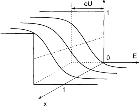
To access the interaction between quasiparticles in a diffusive metal, we have implemented an out-of-equilibrium situation, by placing a diffusive metallic wire between two thick metal pads biased at different electrochemical potentials. Since the energy exchange between quasi-particles tends to establish a local equilibrium, the quasiparticle energy distribution function along the wire should be sensitive to interaction. The practical set-up is sketched in Fig. 1.1.
A wire of length L is connected to two thick pads which act as reservoirs of quasiparticles: they inject in the wire quasiparticles distributed in energy according to a Fermi function at the
tem-1.2 Interaction between quasiparticles in a diffusive wire
Fig. 1.1. Schematics of the experimental layout: a metallic wire of length L is connected to two thick pads at electrochemical potentials differing by eU. The energy distribution function in the wire is deduced from
the differential conductance of the tunnel junction formed between the wire and a superconducting electrode placed underneath.
perature of the crystal and with an electrochemical potential given by the voltage of the pad. These quasiparticles diffuse from one pad to the other in a typical diffusion time TD = L2/ D.
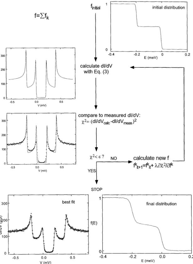
The experiment is based on the strong dependence of the shape of the quasiparticle energy dis-tribution function upon the amount of energy exchanged between the quasiparticles during the diffusion time. The experiment is performed at low temperature, so that the only mechanism leading to a redistribution of the quasiparticle energy is quasiparticle-quasiparticle interac-tion. The distribution function is measured at a given position by a superconducting tunnel probe. The differential conductance of this tunnel junction, deconvolved by the superconduct-ing density of states, yields the energy distribution function.
We have determined in this way the distribution function in the middle of three diffusive wires, differing by their length or the value of their diffusion constant. The functions, measured at a temperature of 30 mK and with a potential difference U
=
0.2 m V applied between the pads, are plotted as continuous lines in figure 1.2. The three curves differ distinctly. The distribution function in the middle of a 1.5 /-lm-long wire (top panel) is close to a step function (dotted curve), which corresponds to the half sum of the boundary distributions. Such a step function is expected if the energy of the quasiparticles is entirely conserved over the duration of their diffusion across the wire. The slight rounding of the measured distribution is a sign that some interaction has occurred. The distribution plotted in the central panel corresponds-Chapter 1 Introduction
1.0
~===::~---'----I - - Experiment cxxxxxxxxr Theory L=1.5!JIll 0=65cm2/s0.0
1.0~~:::::=========~~~~
0.5
0.5
f(E)
......
~
•.•••... ';,~,.
. . L=5!JIll 0=65cm2/s0.0
~===============================~
1.0
1-""-_.._..0.2
-0.2
0.0
E (meV)
L=5!JIll 0=45cm2/s0.0
L---L_---l._----'-_-L---=~~::i-0.4
0.5
Fig. 1.2. Continuous curves: energy distribution function in the center of three different copper wires. Top panel: 1.5 11m-long wire of diffusion constant D = 65 cm2/s. Middle panel: L = 5 11m, D = 65 cm2/s.
Lower panel: L = 5 11m, D = 45 cm2/s. All three wires were45 nm thick and 110 nm wide. The potential difference applied between the two reservoirs isU = 0.2 mV. Measurements were performed atT =30 mK. Symbols: distributions computed using TO = 1 ns (wires with D = 65 cm2/s) and TO = 0.5 ns (wire with
D = 45 cm2/s). Dotted curve in top panel: distribution expected if the quasiparticles do not interact during the entire time of their diffusion across the wire.
1.2 Interaction between quasiparticles in a diffusive wire
to a 5 ILIn-Iong wire fabricated simultaneously. Its diffusion constant should thus be identical to the one of the previous wire, so that electrons take roughly ten times longer to diffuse from one end of the wire to the other. Indeed this curve is more rounded than the previous one, a sign that interaction has caused some redistribution of the electronic energy. The last curve was measured in the middle of a 5 ;'-Lm-Iong wire as well, but with a diffusion constant 40% smaller. This distribution can be fitted by a Fermi-Dirac distribution at a temperature
T = 665 mK, within 5% of the temperature expected if electrons thermalize in each point of the wire.
These results demonstrate the interaction between quasiparticles, and provide the energy relaxation rate, which is of the order of the inverse diffusion time across the second wire 1/TD2 ~ 1 ns-l
.As we shall see, they also give the energy dependence ofthe interaction law: we find an interaction rate inversely proportional to the square of the energy exchanged between quasi particles. The proportionality coefficient can be interpreted as a typical interaction rate
Tal. We determine this rate by fitting the distributions computed with such an interaction law to the measured curves. The symbols plotted in Fig. 1.2 are distributions computed with times TO of respectively 1 and 0.5 ns.
These results indicate that interaction is quite sensitive to the diffusion constant of the metal. In addition, the energy dependence of the exchange rate given by the experiment is not the one predicted by the standard theoretical calculations. This rate would imply a finite quasiparticle lifetime of approximately TO, even at low energy. To account for this result, we
present a model in which the diffusive wire is decomposed into an array of small resistors. Each elementary resistor is the source of a fluctuating current, function of the local quasiparticle distribution. The interaction corresponds to the absorption by a second resistor of part of the power emitted by the first.
-Chapter 1 Introduction
1.3
Density of states in a normal metal in contact with
a superconductor
The single particle density of states, 'toe. the number of states per unit energy and unit
volume of a system, is possibly the physical property which best exhibits the correlations in a metal. Any deviation from a constant density of states as a function of energy (for energies small compared to the Fermi level) is the sign of correlations between two or more quasiparticles. For instance, there are no states below a threshold energy (the gap) in a superconductor, whose ground state consists of paired quasiparticle states at low energy. In
Fig. 1.3. Scanning electron micrograph of the proximity sample, made of two similar circuits. In each circuit, a normal copper wire (N, horizontal) is in good contact with a superconducting aluminum wire (S, diagonal wire on the left). The contact area is the bright region of the NS overlap. The density of states in the normal wires of both circuits is given by the differential conductance of the junctions formed between the normal wires and three normal probes (vertical), labeled Fl , F2 and F3 . The bright areas are the junction
regions.
order to determine the magnitude and energy and space dependence of the pair correlations induced in a normal metal connected to a superconductor, we have measured the single particle
1.3 Density of states in a normal metal in contact with a superconductor
density of states in a normal metal wire in good contact with a superconducting wire, at different distances from the contact. The density of states is proportional to the differential conductance of a tunnel junction between the wire and a normal metal tunnel probe (see scanning electron micrograph of the structure in Fig. 1.3). We present in Fig. 1.4 the conductances of three tunnel junctions, positioned respectively 100, 200 and 700 nm away from the normal/superconductor interface. For comparison, the differential conductance of a tunnel junction between a BCS superconductor and a normal probe is shown in the inset. It is clear from the comparison that the three densities of states in the normal metal do not resemble those of a BCS superconductor: the proximity spectra contain neither an excitation gap nor a strong singularity. Rather, the proximity effect is characterized by a depletion of single particle states at low energy and an excess density of states somewhere below the superconducting gap energy. A constant density of states is recovered at large energy. Not surprisingly, the curve with the strongest deviations from a normal density of states is that of junction F1, the closest
to the interface. It is depleted at the Fermi level to 55% of the normal value. The densities of states measured by junctions F2 and F3 are depleted to 65% and 95% of the normal value at
the Fermi energy. Ifone defines as a typical pair correlation energy the energy corresponding to the maximal density of states, one finds that this typical energy decreases as the distance to the interface increases. This can be understood in the following way: when a Cooper pair enters the normal metal, the phase difference between the doubly occupied quasiparticle state and the doubly empty state, which is constant in the superconductor, evolves in the normal metal with timet as2Et/li,where 2E is the energy difference between the two states. Since the pair correlations at a given position in the normal metal are determined by the contributions of all diffusive trajectories originating in the superconductor and reaching that position, they will be averaged out at distances of the order of jliD / E. Conversely, the typical energy scale at a distance x from the NS interface is the Thouless energy Eo = h.I)/ x2. This behavior is
well accounted for by the theory of the proximity effect (see lower panel of Fig. 1.4).
-Chapter 1 Introduction
0.3
0.2
theory
experiment
1
o
I I- -I- -~ \...,.-~ ~
-4
3
2
1
o
-1
0.5
-0.3 -0.2 -0.1 0.0
0.1
V (mV)
~
0.5
_ _ u - _..._.L...._L-...J_---L_...L_-L._-'-_..._.L...._L----LJFig. 1.4. Top panel: Conductance of tunnel junctions F1 , F2 and F3 , placed respectively 100, 200 and
800 nm away from the NS interface, normalized by the junction conductance at voltageV = 0.3 mY. The conductance is proportionnal to the DOS in the copper wire in good contact with the aluminum wire. Inset: normalized differential conductance of a tunnel junction between a normal probe and a superconducting aluminum wire. All measurements were performed at T =30 mK. Bottom panel: predicted DOS using the theory of the proximity effect, calculated with a spin-flip scattering time ofTsf =65 ps.
1.4 Coherent transport at an NS boundary: the NS-QUID
1.4
Coherent transport at an NS boundary: the
NS-QUID
The subgap (or Andreev) current through a normal metal/superconductor tunnel junction
IS another indicator of the pair correlations in the normal metal. Indeed, this current is
exclusively due to pairs of normal electrons tunneling into the superconductor. Since this tunneling of a pair is a second order process in barrier transmission, the current across opaque barriers should be negligible. However, tunneling attempts by pairs of electrons in
time-reversed states add up coherently, in contrast with the incoherent tunneling attempts of a single electron (see Fig. 1.5). Therefore the Andreev current should be enhanced in a metal where impurities or boundaries confine the electronic trajectories near the NS interface, and all the more so as the coherence time in the normal metal is long.
N
2e
s
Fig. 1.5. Semiclassical representation of the mechanism responsible for constructive interference in the tunneling of pairs of normal electrons. Two weakly localized electrons in the normal electrode with nearly time-reversed wave functions tunnel through the barrier at different points with the same total phase. Ifthe order parameter of the superconductor is uniform, the tunnel amplitudes at these different points contribute constructively to the total current.
Inorder to probe the quantum coherence of electrons in the normal metal, we have devised an interference experiment with two superconducting/normal tunnel junctions in parallel. The relative phase of the two superconducting electrodes is controlled by applying a magnetic field perpendicular to the plane of the loop they form (see Fig. 1.6 for the electron micrograph of three such NS-QUIDs, which differ only by the length of normal wire separating the two tunnel
-Chapter 1 Introduction
junctions). The interference pattern is the conductance of the structure, which is sinusoidally modulated by the field. Figure 1.7 shows theIVcharacteristics of three NS-QUIDs, measured
Fig. 1.6. Scanning electron micrograph of a sample containing three NSQUIDs: each device is made of an open superconducting aluminum loop (upper shadow of the loop), oxidized to form two tunnel junctions with the normal copper wire (lower grey shadow of horizontal wire). The three devices differ only by the distance between the two tunnel junctions.
respectively with no magnetic flux (maximal subgap current), and one flux quantum (minimum subgap current) in the loop.
The modulation of the current by the magnetic field, measured at one point of the IVcurve of one NS-QUID, is shown in the panel below. The modulation is perfectly sinusoidal. In addition, in all three NS-QUIDs, the magnitude of the modulated current (difference between the current with a superconducting phase difference of 0 and
1f)
is of the order of the total current through the structure. The intensity of the modulated current as a function of voltage is shown in the right panel of Fig. 1.7. The maximal current at low voltages, and the decrease in current modulation at high voltage illustrate the loss of coherence between electron pairs with non negligible energy difference. The difference in modulation intensity between the three NS-QUIDs at low energy demonstrates the existence of inelastic processes, such as scattering1.4 Coherent transport at an NS boundary: the NS-QUID
Fig. 1.7. Top panel: IV curves of three interferometers with tunnel junctions separated by 410, 620 and 785 nm respectively; with zero magnetic field (maximal subgap current) and one half flux quantum (minimal current) in the loop. The three sets of curves have been offset vertically for clarity. Lower panel: modulation of the current through an interferometer, for a given voltage, by a magnetic field H applied perpendicularly to the loop of surface A (symbols). The continuous curve is a cosine fit to the data. Right pannel: measured modulated current (symbols) compared to the current computed from the semi-classical probability to diffuse from one junction to the other (continuous lines). All measured curves were taken at T=30 mK.
-Chapter 1 Introduction
by magnetic impurities, which limit the coherence of electron pairs in the normal metal. From the measured curves, a coherence time of about 100 ps, corresponding to a coherence length of about 1 f.Lm, is inferred. The specific shape of the modulated current of all three devices can be deduced from an Andreev rate given by the Fermi golden rule. This current can also be calculated with the theory of the proximity effect. In that framework, the current is due to the existence of pair correlations induced in the normal metal by the presence of the superconductor. This experiment illustrates how Andreev reflection and the proximity effect are two aspects of the same phenomenon.
REFERENCES
[1] D. Pines, P. Nozieres, The theory of quantum liquids (W.A. Benjamin, New York, 1966). [2] M. Tinkham, Introduction to Superconductivity (Me Graw Hill, New York, 1985), chapter 3. [3] P. G. de Gennes, Superconductivity of metals and alloys (W. A. Benjamin, New York, 1966). [4] V. T. Petrashov, V. N. Antonov, P. Delsing, and T. Claeson, Phys. Rev. Lett. 70, 347
(1993); See also Procedings of the NATO Advanced Research Workshop on Mesoscopic
Superconductivity, F. W. J. Hekking, G. Schon, and D. V. Averin, Editors (Elsevier, Amsterdam, 1994).
Chapter 2
Experimental techniques
2.1
Sample fabrication
In the following we describe the different steps leading to a sample in its final form before measurement. Most of these steps use by now standard nanofabrication techniques. The basic principle is to fabricate a mask with carefully designed openings overhanging above a substrate, and to deposit the metals composing the circuit through this mask. By depositing the various metals at different angles, and possibly allowing for an oxidation step, one can implement on the substrate a complex circuit which includes contacts and tunnel junctions between different metals.
The typical fabrication scheme is outlined in Fig. 2.3. The process begins with the coating of a 2-inch oxidized silicon wafer with two layers of electrosensitive polymers (bilayer process), which can be separated by an intermediate germanium layer (trilayer process). The coated wafer is then cut into small chips, which are processed individually. A chip is first exposed to the electron beam of a scanning electron microscope, scanned according to a predefined pattern. The polymer chains exposed to the beam are broken, so that when the chip is developed after exposure only the non exposed regions of the top layer remain. If the chip is made from a wafer coated with a bilayer, the developed top polymer layer constitutes a suspended mask. In the trilayer process, the pattern in the top layer is transferred to the germanium layer through etching. The etched germanium layer then constitutes the mask. In both techniques, the bottom polymer layer acts as a ballast which sustains the mask. The
Chapter 2 Experimental techniques
next step is the deposition of metals through the mask at different angles, and oxidation in between if necessary. The undercut under the mask, due to the greater electrosensitivity of the bottom layer, determines which projections of the mask openings fall onto the substrate and which are projected on the edges of the ballast layer. After deposition, both the mask and the ballast are lifted off in acetone, leaving the circuit deposited on the substrate.
Although the trilayer technique involves a greater number of steps, it is preferred when long, fine structures are needed. Indeed, because of its rigidity, the germanium mask can be suspended over greater lengths than a polymer mask. In addition, the details obtained with a trilayer are usually finer because the electrons backscattered in the thin germanium layer do not widen the exposed areas, and because the electrons backscattered in the ballast and in the silicon substrate are prevented from reaching the top layer by the germanium.
2.1.1
Wafer preparation
We now detail the fabrication process.2.1.1.1 Bilayer coating
In the bilayer technique, the substrate is first coated with a "ballast" layer, whose role is to sustain the second layer, which will constitute the mask, as well as enable an undercut under the openings in the mask. To that end, the bottom layer is a copolymer, whose chains are more easily broken by exposure to the electron beam than those of the top polymer layer. The thickness of the bottom layer is determined by the height at which the mask should hang over the substrate. We have used the following coating procedure:
..
f H f-•
oxidized silicon -substrate
Fig. 2.1.
Bottom layer: copolymer polymethyl-meta-acrylate/meta-acrylate acid (PMMA /MAA) diluted at 70 g/l in 2-ethoxyethanol, filtered with 0.2 !Jm filters. Spun at 850 rpm for about 50 s, and baked on a hot plate at 180 °C for 10 mn; thickness rv 0.5 uus. We use PMMA of
2.1 Sample fabrication
PMMA
~
. . . , r -Ge~
g8
~~
MAAb a l l a s t "
0.8-1urn
oxidized silicon _ _~ substrate Fig. 2.2.molecular weight 950K in all cases.
Top layer: PMMA diluted at 15gil in methyl isobutyl butyl ketone (MIBK), filtered with 0.2 fJm filters. Spun at 850 rpm for about 50 s, and baked on a hot plate at 170 DC for 25 mn. 2.1.1.2 Trilayer coating
In the trilayer technique, the mask is made of a germanium layer sandwiched between the same two resists as those used in the bilayer technique. Thin germanium layers are required when large deposition angles are desired. On the contrary, in some designs (such as the sample for the experiment on the quasiparticle energy relaxation), one of the projections is not wanted. The germanium layer will therefore be made thick so that selected openings of the mask clog up before the last deposition. The thickness of the germanium mask typically varies between 10 and 50 nm.
We have used the following procedure:
Bottom layer: PMMA/MAA diluted at 90 gil in 2-ethoxyethanol, filtered with 0.2 uu:
filters. Spun at 850 rpm for about 50 s, and baked on a hot plate at 160DC for 15 mn. This produces a ballast layer of thickness rv 900 nm.
Middle layer: 10 - 50 nm of thermally evaporated germanium, at a rate of 0.1 nrn/s in a vacuum of 5 10-6 mbar.
Top layer: PMMA diluted at 15gil in MIBK, filtered with 0.2uu:filters. Spun at 850 rpm for about 50 s, and baked on a hot plate at 150DC for 15 mn. As described in [1] , this layer should be baked at a temperature slightly inferior to the baking temperature of the first layer, in order to limit the stress between layers. Without this precaution, characteristic circular cracks may appear in the thin germanium layer.
-Chapter 2 Experimental techniques
2.1.2
Processing of a single chip
The coated wafers are diced into 8 x 8 mm' chipswith a diamond-tip scriber, and each chip is then processed separately.
2.1.2.1 Exposure to electron beam
The patterning of each chip is done with the beam of a JEOL 840A scanning electron mi-croscope. The exposure pattern, dose and blanking of the electron beam are commanded by the Proxy-writer system from Raith GmbH. We currently use a beam acceleration voltage of 35 kV, for which the standard exposure dose is about 2 pC /fLm2.
Principle of electron beam lithography
The principle of the lithography of a multilayer chip with an electron beam is straightforward. Electrons focused onto the sample penetrate both the polymer and copolymer layers (and the Ge layer when there is one). Their energy is released in the resin, breaking the PMMA and MAA into fragments of smaller molecular weight, which are dissolved in the developer in a subsequent development step. As pictured in Fig. 2.3, a broader region in the MAA layer is fragmented by the beam for two reasons. First, the copolymer chains are more easily broken than the PMMA chains. Second, electrons scattering in the MAA layer as well as those backscattered from the substrate contribute to the profile. Thus a lower dose is sufficient to break chains in the MAA layer without damaging the PMMA layer, thereby enabling the realization of a mask with fine openings on top of a sustaining layer with large undercuts. Below we explain how the undercut can be precisely patterned, thereby enabling the fabrication of more elaborate circuits than previously.
Accurate control of the undercut through a two-step exposure sequence
All the samples measured in the course of this thesis were fabricated by depositing through a suspended mask materials at different angles. When the materials are deposited at more than two different angles, undesired contacts or junctions in parallel with the structure to be measured almost unavoidably are produced. This happens because the undercut is symmetric around the openings of the mask, and has an extension which is not controlled. In order to prevent parasitic images, we have developed a two-step exposure sequence which enables an asymmetric undercut of controlled extension, thereby allowing the deposition on the substrate
2.1 Sample fabrication
Lithography Lithography
PMMA with a bilayer with a trilayer / ' PMMA
< , ~ // /./ »> Germanium
MAA ballast -
~
- MAA ballastoxidized silicon>" --- oxidized silicon
exposure to e-beam
standard dose exposure
c-development
overhanging PMAAmask
anisotropic dry etching
~
isotropic dry or wet etching
overhanging Ge mask
metal deposition through mask
second evaporation
~
lift-off
Fig. 2.3. Sequence of steps leading to the fabrication of circuits with the technique of deposition through a suspended mask of PMMA (bilayer technique) or germanium (trilayer technique). The exposure stage of the trilayer process comprises a first standard dose exposure which draws the fine patterns of the mask. A second exposure at low dose patterns the undercut regions.
-Chapter 2 Experimental techniques
of certain mask openings while sending other projections into the ballast layer. The first step is the usual patterning of the finer outlines of the mask, with standard exposure dose. This delimits a small, limited undercut region. The second step patterns the undercut region to the exact desired extension. To that end, the regions delimiting the desired undercut are exposed with a low dose (typically 25% of the standard dose). This suffices to break the ballast copolymer chains but leaves the top PMMA layer undamaged. As an example, the exposure pattern of the sample measured in the experiment on the quasiparticle energy relaxation, and the pattern for the proximity effect experiment will be detailed in section 1.1.3.
2.1.2.2 Development
Bilayers are usually developed for 35 s in a solution of MIBK diluted at 25% vol. in propanol-2, and rinsed in propanol-2. The suspended mask is then ready for the metal deposition step.
Trilayers can be developed either similarly, or for 10 s in a solution of cellosolve (glycol ethyl monoethyl ether), diluted at 30% vol. in methanol, and rinsed in propanol-2. This development only dissolves the fragments in the top layer since the solvent cannot reach the MAA layer, which is protected by the germanium. The undercut in the MAA will be realized through a wet etching step subsequent to the transfer to the germanium of the pattern in the PMMA.
2.1.2.3 Etching of the germanium layer (trilayer process)
The openings in the PMMA are transferred to the germanium layer by an anisotropic reactive ion etching of the sample in a low-pressure SF6 plasma. (SF6 throughput 5 standard cube centimeter per second (seem), P
=
2 X 10⁻³ mbar, accelerating voltage V=
100 V, 40 to80 s-long etch. It is extremely useful to monitor this step with laser interferometry, in order to avoid broadening the openings in the mask). The copolymer layer is then etched in an anisotropic oxygen plasma(02 throughput 10 seem, P
=
2X 10⁻³ mbar, V=
300V, duration8 min). Ifregular undercuts are needed, this anisotropic etch can be followed by an isotropic etch in a high-pressure oxygen plasma (02 throughput 10 seem, P
=
0.1 mbar, V=
100 Vduring 10 min). Iflarge undercuts are needed, it is best to perform a wet etch by dissolving the exposed MAA fragments in MIBK-propanol-2, at room temperature for 20 to 80 s. However, fine copolymer fragments may then remain in the fine mask openings. These are removed easily by a 5 mn-long anisotropic dry etch with the same parameters as previously.
2.1 Sample fabrication
2.1.2.4 Metal deposition and oxidation
Once the mask is completed, the deposition of metals and fabrication of tunnel barriers proceed in an electron gun evaporator. The sample is positioned on a tiltable sample holder. Metals are deposited in a pressure of 10-6 mbar, at a typical rate of 1 nm/s, The principle of the
evaporation is sketched in Fig. 2.4 for the example of a deposition at two angles through a single slit. Contacts or junctions between different materials are obtained by deposition
suspended mask • ballast • substrate • d
=
2 h tan 8 I I'. .'
Id
.
undercutFig. 2.4. Principle of the metal deposition at two angles through a suspended mask.
through several slits, as shown in Fig. 2.3 and 2.5. The first shadow of one slit overlaps with part of the second shadow of the other slit. Tunnel barriers are formed by introducing a few mbar of an oxygenlO%-argongO% mixture between depositions of the materials forming the overlap, thereby oxidizing the first metal. After deposition, the sample is placed in a bath of acetone at 50°C until the resist and the mask are lifted off. The contacts and junctions are then tested at room temperature, by measuring the circuit resistances in parallel with a variable resistor (0 - 7 6 MD), and connected to a multimeter through 1 MD resistors. In
order to avoid destroying the junctions or melting the long narrow wires, a lead shorting all the connection pads was patterned along with the sample, and opened just before measurement.
2.1.3
Examples: two particular samples fabricated with the trilayer
process
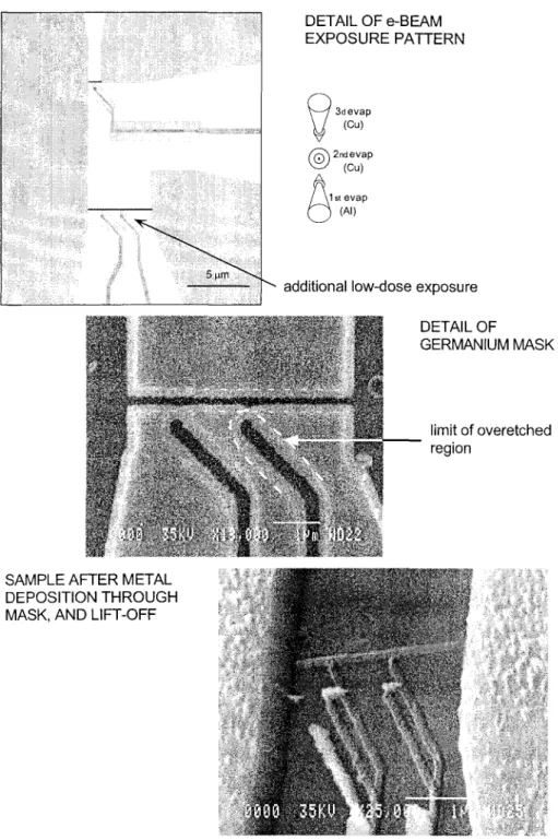
2.1.3.1 Sample measured in the quasiparticle energy relaxation experiment As explained in chapter 4, in the experiment on the energy relaxation of quasiparticles, the
-Chapter 2 Experimental techniques
Oxidation
~
AI deposition
CD
@
Cu depositionAI/AIOxlCu junction
Fig. 2.5. Fabrication of a superconducting/riormal tunnel junction in a two-angle deposition process. In all our experiments, the superconductor is aluminum, the normal metal is copper, and the insulating layer is aluminum oxide.
energy distribution function at a given position of a copper wire was deduced from the con-ductance of a tunnel junction formed between the wire and a superconducting probe. The copper wire itself was connected to two much thicker copper pads which played the role of reservoirs. These different elements were produced by the evaporation of successively 30 nm of Al at a 30° angle (top shadow in the SEM picture of Fig. 2.6), oxidized right afterwards, 30 nm of Cu at a 0° angle, and 450 nm of Cu at a -30° angle with respect to the normal to the sample plane. These materials were deposited through a germanium mask obtained with an exposure pattern described hereafter. The top panel of Fig. 2.6 shows the pattern of exposure to the electron beam, with the doses encoded in shades of grey. The two horizontal lines will produce the 1.5 and 5 ,urn-long copper wires; they are connected to a common large pad to the left (corresponding to the grounded reservoir in the experiment) and to two distinct large pads to the right, which will produce the reservoirs (biased at a finite potential in the experiment). The patterns shaped as crooked fingers below the wires will produce the openings through which the superconducting probes will be deposited. The light shaded areas correspond to a region exposed with a dose of 25% the nominal dose. The key feature of this design is that the regions around the fingers are exposed with this low dose, whereas the regions around the wires are not. The consequence of this can be seen from the SEM picture of a typical germa-nium mask obtained from a chip exposed with this pattern, and presented below: there is a large undercut below the germanium mask around these fingers (light-colored region around
2.1 Sample fabrication
SAMPLE AFTER METAL DEPOSITION THROUGH MASK, AND LIFT-OFF
DETAIL OF e-BEAM EXPOSURE PATTERN
q
3devapV
(Cu) @2ndevap \:':!/ (Cu) T\1st evapo
(AI)additional low-dose exposure DETAIL OF
GERMANIUM MASK
limit of overetched region
Fig. 2.6. Fabrication of a sample for the quasiparticle energy relaxation experiment. Top: exposure pattern of the center of the chip, with dose encoded in levels of gray. The arrows indicate schematically the order and angle of deposition of the different metals. Middle: micrograph of the Ge mask on the copolymer, after development and etch of the exposed trilayer. Dark regions correspond to the silicon substrate seen through the openings of the mask. Light regions around the openings delimit the undercut region. The regions around the vertical fingers have had an additional low dose exposure, and consequently have a greater undercut. Lower micrograph: actual sample, seen at an angle, obtained by deposition of Al at 30°, oxidation, and Cu depositions at 0 and -30° relatively to the normal to the sample, through a mask such as the one figured above, although probably with broader overetched regions.
-Chapter 2 Experimental techniques
the dark openings, due to the absence of MAA under the germanium), whereas the undercut around the opening of the wire is much smaller. As a result, only the vertical copper depo-sition will project the image of the wire opening onto the substrate. The upward aluminum deposition will send the projection of the wire opening into the ballast resist, thereby avoiding an unwanted aluminum projection which would have been in parallel with the copper wire. The same could in principle be expected of the shadow produced by the downward copper deposition. But as can be seen from the SEM micrograph of the finished sample, traces of a shadow below the wire do appear due to the extra-dose boxes around the fingers. On the con-trary, the projection of the finger openings during the upward aluminum deposition is wanted in order to produce the aluminum tunnel probes, which explains why some areas received an extra dose. The copper projection obtained with the vertical deposition is of no nuisance. The image obtained with the last downward deposition could be a problem, however, because of the thickness of this last Cu deposition. Thick images of fine details can prevent a proper lift-off of the resist. To avoid such problems, the deposition angles were chosen large, so that the fine openings clog up well before the entire 450 nm of Cu have been deposited through them. Clogging is insignificant for the large pads, through which the reservoirs are deposited on each side of the wires in the last downward evaporation.
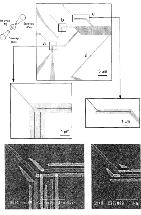
2.1.3.2 Sample for the proximity effect measurement
This sample comprised four different elements (see Fig. 2.7). The two first elements were two similar circuits (labeled a and b, where a is pictured at the bottom) made of a superconducting aluminum wire (wire at an angle in the picture) in good contact with a normal copper metal wire (horizontal). The density of states in the copper wire at a given position was probed by measuring the conductance of the tunnel junction formed by this copper wire and another copper wire (vertical in the picture) overlapping the wire at that position. Two such tunnel probes were fabricated in the circuit shown in the SEM photograph (corresponding to exposure pattern a), and a probe placed at an intermediate position was fabricated on the second circuit (exposure pattern b). These two circuits require a good NS contact and an NIN tunnel barrier. A third element of the sample was a reference NIS tunnel junction, designed to measure the density of states of the superconductor. The fourth element (d) was a long SNIN sandwich, the critical temperature of which provided a lower limit for the transparency of the NS contact.
2.1 Sample fabrication
All these elements were produced by tilting the sample counterclockwise by 45° in its plane, and depositing the normal and superconducting metals at three angles respectively to the sample plane. The first deposition was a 20 nm evaporation of aluminum normally to the sample plane, immediately followed by the deposition of 25 nm of copper at a -20° angle. In this experiment, a tunnel junction with normal electrodes in zero magnetic field was required, since the proximity effect is destroyed by a weak magnetic field. Therefore the usual AI-Ab03-Al junctions could not be used. Instead we fabricated Cu-AI203-Cu junctions, by depositing
thin Al layers and then oxidizing them completely. We first deposited a 1.4 nm-thick layer of Al at a -20° angle, in a He pressure of 10-4 mbar in order to insure an isotropic deposition of the AI. Without this precaution, the sides of the Cu electrodes may remain uncovered, resulting in shorts. The Al was then oxidized in a 80 mbar mixture of oxygen (10%) and argon (90%) for 10 min. This sequence was repeated at an angle of20°. We then deposited 30 nm of copper at a 20° angle. Figure 2.7 explains how the different features could be obtained with this sequence. The top box figures the e-beam exposure pattern of the center of the chip, done at magnification 1000, with the doses encoded in shades of grey. The patterns denoted by a and b are the proximity circuits, of which a is magnified below. The light gray region corresponds to the region which is exposed with 25% of the nominal dose, and thus gives the extension of the region under the germanium mask where the MAA will be removed. As can be seen in the SEM photograph below, the consequence is that the three projections of the vertical openings are reproduced on the substrate, and so are the three projections of the horizontal wire. On the contrary, only the central shadow of the tilted opening extends continuously from the contact with the horizontal wire to the lead. The side shadows are projected onto the substrate only near the contact region, but are projected onto the resist further out, and thus are stripped off in the lift-off process.
The pattern denoted by c, and magnified below, is the pattern which produces the NIS tunnel junction pictured in the bottom right SEM micrograph. As in the proximity circuit, the superconducting wire is the tilted central shadow. But in this device, it is not covered by the copper wire immediately deposited after the aluminum (lower horizontal shadow). Instead, because of the relative disposition of the two openings in the mask, the superconducting wire is oxidized in all three oxidation steps and then covered by the top projection of the horizontal
-Chapter 2 Experimental techniques 1stevap
n
(AI)~ndeVap
&
(Cu) cY:ctevap (Cu)Fig. 2.7. Steps in the fabrication of the sample measured in the experiment on the proximity effect. Top: exposure pattern of the central part of chip. Circuits a and b: proximity circuits; c: pattern leading to the reference SIN junction; d: strip leading to the NS sandwich. The arrows represent the order and angle of deposition of the various metals. Bottom: Left: SEM micrograph of finished circuit a. Right: SEM micrograph of finished circuit c.
2.1 Sample fabrication
openmg. Here also, because of the absence of low dose box around the tilted opening, the lower shadow, which would otherwise form a good SN contact in parallel with the SIN junction, is stripped away.
Finally, the materials deposited through the opening in the mask produced by the exposure of the strip labeled d will overlap in a central region, forming a SNIN sandwich, the resistance of which will be measured as a function of temperature.
-Chapter 2 Experimental techniques
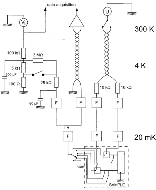
2.2
Sample measurement at low temperature
The chip is glued with silver paint to a thin copper plate fixed onto an integrated circuit connector, which plays the role of the sample holder. The pads of the circuit are connected to the pins of the connector with 25 /-lm-wide gold wires, using ultrasonic bonding. The sample holder is then plugged into a socket installed in a copper box thermally anchored to the mixing chamber of the dilution refrigerator. The chip is thermally anchored through a copper braid tightly screwed onto the copper plate of the sample holder. The sample box and the last stage of electrical filtering lie in another shielded copper box anchored to the mixing chamber of the dilution refrigerator. The sample box contains a small superconducting coil, which was used to apply a small magnetic field to the NS-QUIDs.
Electrical connections to the sample are made through filtered coaxial lines (see Fig. 2.8). Lossy inductive filters as well as microfabricated distributed RC filters [2] are used. They are carefully anchored to the dilution refrigerator, thereby insuring the thermalization of the electrical lines. The current-voltage characteristics of the sample are obtained by measuring the voltage drop across the sample in series with the last stage filter, amplified at the output of a twisted pair by a low-noise, battery powered pre-amplifier (Ithaco model 1201), as a function of current. The current I in the sample is produced by applying an input bias voltage Vb to a bias line consisting of a voltage divider in series with a resistance. According to the desired load line, this resistance can be switched to either 3 MO or rv 30 kO with a mechanical switch
in a shielded box in the helium bath at 4 K. The current is thus not directly measured, but is calculated from the input voltage, the measured voltage on the sample and the resistance values of the filters and resistors in lines, which are determined at each cool-down. To measure differential di/ dV (V) conductance curves, a small AC component is added to the DC bias voltage, and a lock-in detection is performed with a SR830. The bias and output voltages were recorded on a digital oscilloscope (Nicolet.Prod-l}.
An important feature of the measurement apparatus is the possibility to measure in one cool-down several circuits with a single bias line and a single twisted pair. To this end, the output of the last filter common to the bias and measuring lines is connected to a 12-position commercial commutator in which the friction was minimized, of which every other position is wired to the sample. The positions are marked by six resistors of known value connected
2.2 Sample measurement at low temperature data acquisition 600pF
1
' 00 0300 K
4K
20 mK
1- _Fig. 2.8. Schematics of the electrical wiring of the experiment inside the dilution refrigerator, in the case of the quasiparticle energy relaxation experiment. The current through the sample is supplied by a bias voltage Vb applied to a resistance of 3 Mil or 25 kll. The voltage across the sample in series with a filter F is brought to a preamplifier at room temperature through a twisted pair. An additional twisted pair is used to bias the meso scopic wire to a voltage U.
-Chapter 2 Experimental techniques
in between. Positions are switched by a motor (ESCAP, M915L61) anchored to the still of the dilution refrigerator. The commutator itself is thermally anchored to the mixing chamber. Transmission between motor and commutator is done with a plastic fiber. Commutation produces a 20-50 mK rise in temperature.
A second twisted pair was added between room temperature and the 1 K pot (see Fig. 2.8), in order to enable measurements of small resistances. Following the technique of D. C. Glattli
et at. [3] adapted by P. Joyez, this twisted pair consists in two intertwined micro coaxial cables. Each coaxial cable is made of a manganin wire of diameter 0.1 mm (resistance rv
60 Dim) coated by a polyimide insulating layer, glued into a stainless steel tube of internal diameter 0.4 mm and external diameter 1 mm. This cable has a distributed capacitance of about 20 pFjm. A 10 kD resistance was added at the bottom end of the cable, producing a cut-off frequency of 200 kHz. Both lines of the pair were also used as independent bias lines, for instance in the case in the experiment on the quasiparticle energy relaxation (see Fig. 2.8).
REFERENCES
[1] V. Bouchiat, Ph.D. thesis, Universite Paris 6 (1997).
[2] D. Vion, P. F. Orfila, P. Joyez, D. Esteve, and M. H. Devoret, J. Appl. Phys. 77, 2519 (1994).
[3] D. C. Glattli, P. Jacques, A. Kumar, P. Pari and L. Saminadayar, J. Appl. Phys. 81, 7350 (1997).
Chapter 3
Observation of energy redistribution
between quasiparticles in mesoscopic
•
WIres
3.1
Can the interaction between quasiparticles be
probed?
Electrons in metals constitute the most common example of a Fermi fluid. Despite the underlying complexity of this many-body interacting system, the independent electron model can quantitatively account for most properties of bulk metals, provided that proper effective parameters are chosen for the electrons [1]. The explanation of this amazing simplification is due to Landau who showed that any fluid of interacting fermions maps onto a fluid of independent fermions, the Landau quasiparticles. A quasiparticle excitation involves a many-body rearrangement of the electron ground state wave-function. The residual interaction between quasiparticles is small because the interactions between the real particles are almost completely encapsulated inside each quasiparticle. An "electron-like" quasiparticle can be viewed as an extra electron surrounded by a screening cloud. The Coulomb interaction between electrons is thus replaced by a screened Coulomb interaction between quasiparticles.
The theory of Fermi liquids [2], which extends Landau's pioneering work, succeeds in pre-dicting the quasiparticle spectrum, the response to external fields, and the residual interaction between quasiparticles, which is well described by two-body quasiparticle-quasiparticle
scatter-Chapter 3 Observation of energy redistribution between quasi particles in rnesoscopic wires
ing. It gives a finite width to the quasiparticle levels, and provides an internal thermalization mechanism for the quasiparticles. Ina metal with perfect crystalline arrangement, the width of a level of energy E above the Fermi energy is predicted to follow a E2 law, so that
quasi-particles at the Fermi level are perfectly defined. Inthe case of metals in which quasiparticles undergo elastic scattering by impurities or by the sample surface, the theory of diffusive con-ductors developed in the 80s by Altshuler and coworkers [3] predicts a series of different behaviors, which depend on the energy considered compared to the Thouless energies charac-teristic of the sample dimensions. In all cases, it predicts that, unless the elastic scattering is extremely important, quasiparticles are still well defined excitations near the Fermi energy. Evidence for the existence of a residual interaction is provided by the observation of quasipar-ticle thermalization in samples cooled below lK. Indeed, whereas at temperatures above lK quasiparticles and phonons are well coupled so that the quasiparticles are directly thermalized by the phonons to the phonon temperature, the two systems are decoupled below lK. The ex-periment described in this chapter provides direct evidence for energy redistribution between quasiparticles , and gives access to the corresponding scattering rate.
Inorder to observe energy redistribution between quasiparticles , one must bring the con-ductor which contains them out of thermal equilibrium. We have implemented such a situation by placing a thin wire between two thick electrodes biased at different potentials. These elec-trodes act as quasiparticle reservoirs [4]: they absorb all incoming quasiparticles, and emit quasiparticles with an energy distribution given by their own Fermi distribution. Quasipar-ticles interact while they diffuse across the wire. Since the energy redistribution process is expected to affect the energy distribution function of quasiparticles at all points in the wire, one can in principle extract the energy redistribution rate between quasiparticles by measuring this distribution in a few points along the wire. Inour experiments, the energy distribution at a given position wire is deduced from the conductance of a tunnel junction between the wire and a superconducting electrode underneath. Information on the energy-dependence of the energy redistribution rate is only accessible if measurable redistribution occurs, but is still too weak to establish thermal equilibrium. We have fabricated samples with different diffusion times, in order to cover the whole range of possible regimes, from the non-interacting case to the fully thermalized one. These limiting regimes are discussed in the next section.
3.2 Energy distribution function of quasiparticles in a meso scopic diffusive wire
3.2
Energy distribution function of quasiparticles
mesoscopic diffusive wire
.
In a
We choose as the reference energy the electrochemical potential of the reservoir situated at
X
<
O. When the reservoir at X>
L is biased at potential U, its electrochemical potential is-eU.
Fig. 3.1. Principle of the experiment: a wire of length L is connected to two thick and large electrodes. A bias voltage U is applied between the electrodes.
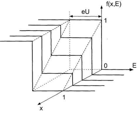
The distribution functions in the reservoirs are therefore Fermi-Dirac functions at the tem-perature T of the reservoirs, shifted in energy by eU. The shape of the distribution function
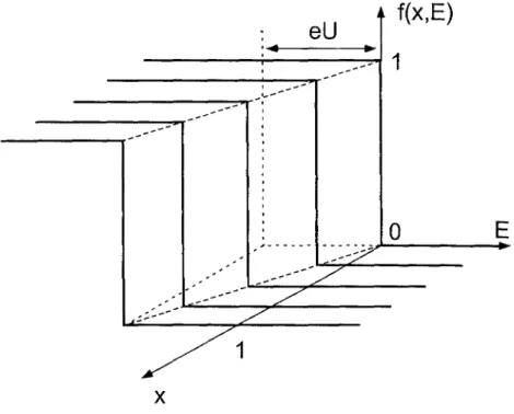
f(x, E) in the wire at position x
=
XI
L is determined by the diffusion and the inelastic scat-tering processes. We consider here the different quasiparticle scatscat-tering mechanisms occurring in metals: scattering by phonons and scattering by quasiparticles. Several authors have eval-uated the distribution function of quasiparticles for a wire in the different limiting regimes[5-7] , and we hereafter present their results.
3.2.1
No quasiparticle scattering, no phonon scattering
In the absence of inelastic scattering, the total energy of each quasiparticle is conserved along the wire. The distribution function