by
Michael Price
Submitted to the Department of Electrical Engineering and Computer Science in partial fulfillment of the requirements for the degree of
Master of Engineering in Electrical Engineering and Computer Science at the
MASSACHUSETTS INSTITUTE OF TECHNOLOGY February 2009
c
° Massachusetts Institute of Technology 2009. All rights reserved.
Author . . . . Department of Electrical Engineering and Computer Science
February 3, 2009 Certified by . . . . Vladimir M. Stojanovic Assistant Professor Thesis Supervisor Certified by . . . . Michael St. Germain Design Engineer, Analog Devices Inc. Thesis Supervisor
Accepted by . . . . Arthur C. Smith Chairman, Department Committee on Graduate Theses
Michael Price
Submitted to the Department of Electrical Engineering and Computer Science on February 3, 2009, in partial fulfillment of the
requirements for the degree of
Master of Engineering in Electrical Engineering and Computer Science
Abstract
Data-dependent jitter (DDJ) caused by lossy channels is a limiting factor in the bit rates that can be achieved reliably over serial links. This thesis explains the causes of DDJ and existing equalization techniques, then develops an asynchronous (clock-agnostic) architecture for DDJ compensation. The compensation circuit alters the transition times of a digital signal to cancel the expected channel-induced delays. It is designed for a 0.35 µm BiCMOS process with a 240 × 140 µm footprint and typically consumes 3.4 mA, a small fraction of the current used in a typical transmitter. Extensive simulations demonstrate that the circuit has the potential to reduce channel-induced DDJ by at least 50% at bit rates of 6.25 Gb/s and 10 Gb/s.
Thesis Supervisor: Vladimir M. Stojanovic Title: Assistant Professor
Thesis Supervisor: Michael St. Germain Title: Design Engineer, Analog Devices Inc.
Everyone I can think of deserves two types of acknowledgement: thanks for helping me carry out the work leading to this thesis, and thanks for bringing me where I am today. I don’t have the room or the ability to express the latter here. If you know me and you’re reading this, chances are that I love you.
Prof. Vladimir Stojanovic, my thesis advisor, made this process quick and painless. Even though he did not work closely with me, he paid attention to what I was doing and provided the feedback I needed on the important problems. He surprised me by taking extra time to talk about my decision between grad school and industry.
Michael St. Germain, my advisor at ADI, offered friendly advice and gave me so much freedom that I’d feel silly calling him a supervisor. He helped me understand the IC design and fabrication process, went along with my absurd hoopla circuitry, and taught me to shoot the engineer once in a while (which is why this thesis is done).
Kimo Tam, Jen Lloyd and the ADI High-speed Interconnect Group supported me by funding two sum-mer internships and a VI-A fellowship.
Jesse Bankman put a lot of effort into understanding the issues associated with DDJ compensation. He helped me improve both the architecture and the circuitry even though it wasn’t his job.
My fellow interns (Leon Fay, Vinith Misra, Jon Spaulding, Khoa Nguyen, and Henry Wu) and a friendly bunch of engineers (Jeremy Walker, Ben Walker, Andy Wang, Amanda Wozniak, Matt Duff, Stever Lee, and others) made my days at ADI more interesting than the work alone ever could.
My parents let me build and tweak audio electronics when I was in high school, and put up with loud noises, smells, stains and burns so I could teach myself the important things about engineering before arriv-ing at MIT.
Finally, I would like to single out two of my role models, even if they didn’t know they were role models. Their inspiration is hidden in this thesis.
• Prof. Jeff Shapiro, my academic advisor, is incredibly well-organized and rigorous but still manages
to be devoted and inventive. He’s a living example that success in a demanding academic environment doesn’t have to be draining.
• Mike Axiak, a fellow student, is completely unafraid of learning new things and more productive than
anyone else I know. I’ll never match his brilliance, but I’ll be content to be a fraction as easygoing, open-minded, or helpful as he is.
1 Introduction 17
1.1 Serial links . . . 17
1.1.1 Typical link scenario . . . 18
1.1.2 Channel loss mechanisms . . . 18
1.1.3 Jitter . . . 20
1.1.4 Noise . . . 21
1.1.5 Crosstalk . . . 22
1.2 Project summary . . . 23
1.3 Amplitude equalization techniques . . . 25
1.3.1 Transmit equalization . . . 25
1.3.2 Receive equalization . . . 25
1.3.3 Decision feedback equalization . . . 27
1.4 Phase equalization techniques . . . 28
1.4.1 The Buckwalter scheme . . . 28
1.4.2 Jitter histogram representation . . . 29
1.4.3 Reported performance results . . . 29
2 A DDJ Compensation Scheme 31 2.1 Revisiting the Buckwalter scheme . . . 32
2.1.1 Linear system interpretation . . . 32
2.1.2 Interpolating delay coefficients . . . 33
2.2 Characteristic delay . . . 34
2.2.1 Definition . . . 35
2.3.2 Simplifications . . . 39
2.4 Nonlinear methods . . . 40
2.4.1 Nonlinearity in desired delays . . . 42
2.4.2 Mitigating linearity errors . . . 46
2.5 Discussion . . . 47
2.5.1 Compensating transmitter jitter . . . 47
2.5.2 Summary . . . 48
3 Design Review 49 3.1 Top-level overview . . . 49
3.2 Adjustment mechanisms . . . 49
3.3 Characteristic delay emulator (CDE) . . . 51
3.3.1 Variable amplitude input limiter . . . 51
3.3.2 Common-mode feedback . . . 53
3.3.3 RC filters . . . 53
3.4 Ramp generator . . . 54
3.4.1 Concept and implementation . . . 54
3.4.2 Clamp circuit . . . 57
3.5 Common-mode feedback (CMFB) . . . 59
3.5.1 Technique . . . 62
3.5.2 Compensation . . . 62
3.5.3 Clamp range control . . . 63
3.6 Comparator . . . 66
3.6.1 Differential input stage . . . 68
3.6.2 Modified Cherry-Hooper amplifier . . . 68
3.7 Auxiliary circuit blocks . . . 70
3.7.1 Delay cell for CDE input . . . 72
3.7.2 Joint current mirror for CMFB tracking . . . 72
3.8 Layouts . . . 74
4.2 Nominal conditions . . . 79
4.3 Nonideal effects . . . 79
4.3.1 Process skew . . . 79
4.3.2 Temperature and supply voltage . . . 80
4.3.3 Improper adjustment . . . 81
4.3.4 Random device variation . . . 83
4.4 Cooperative equalization . . . 84 4.5 Discussion . . . 88 4.5.1 Benefits . . . 88 4.5.2 Limitations . . . 88 5 Conclusion 89 5.1 Summary . . . 89
5.2 Directions for future research . . . 90
5.2.1 DDJ improvements . . . 90
5.2.2 Effects on DFEs . . . 91
5.2.3 Automatic adaptive pre-emphasis . . . 93
1-1 A serial link. . . 18
1-2 Frequency responses and eye diagrams for 8”, 16” and 24” long FR4 channels. . . 19
1-3 Data-dependent transition delays: A rising edge following a stream of mostly zeros exhibits higher transition delay than a rising edge following a stream of mostly ones. . . 20
1-4 Eye diagram (left) and the corresponding jitter distribution (right). . . 21
1-5 Noise-limited bit rates for a PAM2 link as a function of the comparator resolution Vc. . . 23
1-6 Block diagram of crosstalk between two channels. . . 23
1-7 A serial link with feedforward DDJ compensation. . . 24
1-8 Introducing a delay at the transmitter reduces the data-dependent difference in received tran-sition delays. The uncompensated trace from figure 1-3 (light green) is shown for comparison. 24 1-9 Eye diagrams for uncompensated (left) and compensated (right) 40” FR4 channels at 6.25 Gb/s. . . 25
1-10 Transmit pre-emphasis using a 1-tap FIR filter. . . 26
1-11 A simple buffered passive equalizer for receivers. . . 26
1-12 A DFE receiver. . . 27
1-13 DDJ compensation device designed by Jim Buckwalter. . . 28
1-14 Jitter compensation viewed as an operation on jitter distributions. . . 29
2-1 Delay coefficient vectors of varying length for a 15” FR4 channel at 10 Gb/s. . . 33
2-2 Delay coefficients compared for 10”, 15”, and 20” long FR4 channels at 10 Gb/s. . . 34
2-3 Channel responses (left) and the corresponding characteristic delay responses (right); in the frequency domain (top) and time domain (bottom). . . 36
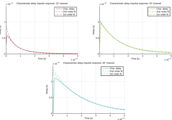
2-4 Characteristic delay functions for 10”, 20” and 30” FR4 channels. 1st- and 2nd-order fits to the impulse responses are also shown. . . 37
2-8 Plots of voltage signals within simplified DDJ compensator. . . 41
2-9 A generalized DDJ compensator to generate nonlinear delays. . . 41
2-10 Plots of voltage signals within nonlinear DDJ compensator. . . 42
2-11 Test cases for determining the nonlinearity of the channel-induced transition delay. . . 44
2-12 Deviation from transition delay linearity for a first-order channel. . . 46
2-13 Scatter plots of the actual vs. predicted transition delays (left) and errors vs. predicted delays (right) for 25” FR4 channel at 10 Gb/s. . . 47
2-14 Frequency responses and characteristic delay functions for FR4 channels modeled with and without the effects of finite transmitter bandwidth. . . 48
3-1 Top-level schematic of DDJ compensator. . . 50
3-2 Concept of CDE filters. . . 52
3-3 Dual variable-amplitude input limiter for CDE. . . 52
3-4 Simple common-mode feedback loop for CDE input limiters. . . 53
3-5 Complete schematic of characteristic delay emulator (CDE). . . 55
3-6 Effect of varying digital input codes on CDE response. Top left: “slow” component. Top right: “fast” component. Bottom: sum of both components. . . 56
3-7 Concept of differential ramp generator. . . 57
3-8 Diode-clamped (left) and actively clamped (right) ramp generator circuits. . . 59
3-9 Effect of MOSFET current source length mismatch on the VCE clamp range. . . 60
3-10 Effect of a base offset current on the VCEclamp range. . . 60
3-11 Complete schematic of ramp generator. . . 61
3-12 Graph showing voltage drops in CMFB scheme. . . 62
3-13 Comparison of standard Miller compensated (left) and degenerated lead compensated (right) CMFB topologies. . . 63
3-14 Open-loop frequency response of a typical CMFB loop with 50 fF Miller compensation capacitors. . . 64
3-15 Open-loop frequency response of heavily degenerated lead compensated CMFB loop. . . 65
3-16 Nested feedback arrangement for clamp VCEand common-mode level control. . . 65
3-20 Block diagram for Cherry-Hooper amplifier topology. . . 69
3-21 Circuits for synthesizing negative differential capacitance loads. . . 70
3-22 Complete schematic of differential comparator. . . 71
3-23 Transient simulation of differential-input comparator. . . 71
3-24 AC simulation of differential-input comparator. . . 72
3-25 Complete schematic of 40ps delay cell. . . 73
3-26 Schematic of adjustable current mirror. . . 73
3-27 Top-level floorplan of DDJ compensator layout. . . 74
3-28 Layout of DDJ compensator. . . 75
4-1 A “bathtub” plot showing the sampling window as a function of desired BER. . . 78
4-2 Peak-to-peak jitter swept against temperature and supply voltage. . . 81
4-3 Predistorted (transmitted) and received signal eyes when compensator is properly adjusted. . 82
4-4 Predistorted (transmitted) and received signal eyes when compensator is improperly adjusted. 82 4-5 Jitter as a function of the control settings: characteristic delay (left) and ramp (right). . . 82
4-6 Distribution of received peak-to-peak jitter due to random device variations. . . 83
4-7 Eye diagrams of ramp output at 10 Gb/s: overly clamped (top left), insufficiently clamped (top right), and normal (bottom). . . 84
4-8 Eye diagrams simulated at transmitter (left) and receiver (right) for 40” FR4 link equalized with 3 dB of FIR pre-emphasis plus DDJ compensation. . . 85
4-9 Transmitter current draw (green trace) and jitter (blue trace) for varying amounts of ampli-tude pre-emphasis (40” of FR4 trace at 6.25 Gb/s). . . 85
4-10 Current/jitter tradeoff for varying amounts of DDJ compensation. . . 86
4-11 Current/jitter tradeoff for combined use of amplitude pre-emphasis and DDJ compensation. . 86
4-12 Eye openings of received signals over 40” of FR4 trace at 6.25 Gb/s, with transmitter current draw (including DDJ compensator) capped at 20 mA. . . 87
5-1 Sampled voltages from a DFE input (light green) and DFE output (blue) for uncompensated (left) and compensated (right) bitstreams. . . 92
5-2 Eye diagrams of ideal DFE outputs for uncompensated (left) and compensated (right) bit-streams. . . 92
1.1 Reported DDJ compensation circuit parameters and performance. . . 30
2.1 Results of simulating test cases using 15” FR4 channel. . . 45
3.1 Optimal settings for digital controls of DDJ compensator in nominal process conditions. . . 51
4.1 Peak-to-peak jitter before and after compensation in six nominal cases. . . 79
4.2 Compensated peak-to-peak jitter in process corners. . . 80
Introduction
Everything in nature is a lowpass filter. Thanks to parasitic capacitances, dispersion of electromagnetic fields, and even Newton’s second law, we are unable to generate signals that change instantly. Were it not for this simple inconvenience, electronic devices could transmit data at arbitrarily high speeds. The bandwidth of the medium between two devices limits the data rates that they can use to communicate.
Modern computers and networking equipment need to process data at several Gb/s, yet the industry relies on particularly low-bandwidth (but inexpensive) copper wires and printed circuit board (PCB) traces. The intersymbol interference (ISI) caused by these low-bandwidth channels results in jitter, which is an uncertainty in the transition times between symbols. A slew of equalization techniques has cropped up to fight bandwidth limitations. Most equalizers alter the shape of transmitted pulses (emphasizing high-frequency components) in order to reduce ISI and jitter in the received signal.
Adjusting the timing of pulses directly can reduce jitter in a more energy-efficient manner. It will be demonstrated below that jitter compensation can be performed by small analog circuits without attempting to recover a clock. The phenomenon of jitter in serial links, along with existing equalization techniques, will be examined first.
1.1 Serial links
Consider a serial link, or high-speed link, to be a digital communications system consisting of a transmitter, channel, and receiver. We will focus on the lowest-level transmission of 1s and 0s, while keeping in mind that the encoding scheme is another important tool for maximizing system performance [2]. Several “channel impairments” establish constraints on the speed and reliability of a link [24]. First and foremost is high-frequency loss: the Nyquist high-frequency for the desired bit rate is typically well above the −3 dB bandwidth
Transmitter Receiver Lossy Channel
Data Out Data In
Figure 1-1: A serial link.
of the channel. As a result, the received signal looks very different from the transmitted one; it may be difficult to recover the exact bit sequence that was transmitted. The remaining sections of this introduction examine the implications of high-frequency loss as well as noise and crosstalk.
1.1.1 Typical link scenario
A typical application of high-speed link technology is found in network routers and switches. These de-vices selectively transmit information between a set of ports connected to computer network adapters and other networking equipment by Category 5 and fiber-optic cables. Inside the router, microprocessors and crosspoint switches on several line card PCBs communicate through traces on the cards, or across a larger backplane PCB. The channel for each link consists of a differential trace across the PCB[s], along with card
connectors and vias.1 This link is shown in schematic form in figure 1-1.
In the context of a modular system, the line cards (and the associated ICs) are replaced more frequently than the backplanes. As IC device sizes shrink and on-chip bandwidth increases, the channel does not necessarily improve. Many serial link design techniques (including jitter compensation) are intended to squeeze the highest possible speeds from this existing hardware.
1.1.2 Channel loss mechanisms
Circuit board traces suffer from skin effect and dielectric loss [6]. An appropriate model for the frequency response of a trace from one end to the other is
H(jω) = exp −l Fjvc |{z} prop delay + (1 + j)p2π2µσω | {z } skin effect + 2π√²rtan δ c ω | {z } dielectric loss
108 109 1010 1011 −30 −25 −20 −15 −10 −5 0 5 Frequency (Hz) Response magnitude (dB)
Channel frequency response: 8", 16", 24" FR4
0 2 4 6 8 10 12 14 16 18 x 10−11 −0.6 −0.4 −0.2 0 0.2 0.4 0.6
Hybrid Line Eye: 8" FR4 channel
0 2 4 6 8 10 12 14 16 18 x 10−11 −0.6 −0.4 −0.2 0 0.2 0.4 0.6
Hybrid Line Eye: 16" FR4 channel
0 2 4 6 8 10 12 14 16 18 x 10−11 −0.6 −0.4 −0.2 0 0.2 0.4 0.6 Time (s) Differential amplitude (V)
Hybrid Line Eye: 24" FR4 channel
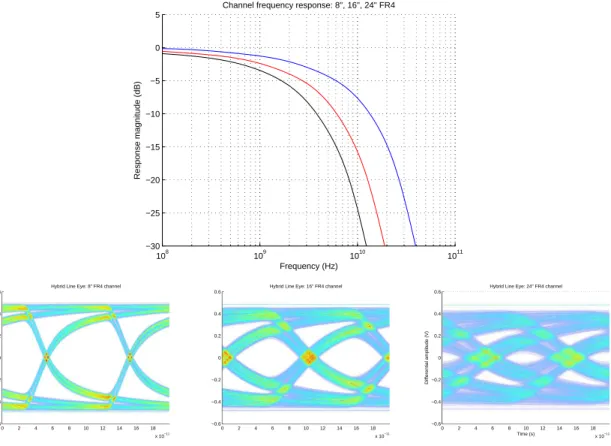
Figure 1-2: Frequency responses and eye diagrams for 8”, 16” and 24” long FR4 channels.
where l and Fvare the length and velocity factor of the trace, µ and ²rare the permeability and dielectric
constant of the dielectric, σ is the conductivity of the trace, and c is the speed of light.
The narrowing of the trace’s effective cross-sectional area (skin effect) contributes an e−√1ω factor to the
channel’s frequency response. A dielectric loss proportional to e−ωtakes over at high frequencies.
Approximate responses of some short FR4 channels and the corresponding eye diagrams are shown in figure 1-2. Response aberrations due to trace discontinuities, connectors, and reflections are not included in the model. These aberrations do contribute jitter, but it is important to concentrate on the bulk loss first. The eye diagrams show that high-frequency loss causes the sampling window to shrink as the channel gets longer.
The propagation delay (e−jtd component) will be ignored from now on, as it has no effect on link
Figure 1-3: Data-dependent transition delays: A rising edge following a stream of mostly zeros exhibits higher transition delay than a rising edge following a stream of mostly ones.
1.1.3 Jitter
Jitter is a timing error in a digital signal—the difference between the expected and actual transition times. When a digital signal (bitstream) is passed through a linear filter and then thresholded, the amplitude dis-tortion introduced by the filter is eliminated but the phase disdis-tortion remains. This operation introduces deterministic jitter in any high-speed link [5].
Consider the case in figure 1-3 of 2-level pulse amplitude modulation (PAM2) where the transmitted signal has a perfectly uniform clock, so the transitions are evenly spaced. When transitioning from 0 (low) to 1 (high) after a long sequence of 0s, the step response of the channel takes about 70 ps to reach the the threshold voltage. This time is the maximum transition delay. When transitioning from 0 to 1 after a sequence of 1s followed by a single 0, the transition delay is smaller (about 40 ps) since the channel has not fully settled to 0 before the transmitted transition. These two transition delays mark the boundaries of the channel-induced data-dependent jitter (DDJ) distribution.
As the deterministic component of the jitter increases, the sampling time required for a desired bit error rate (BER) must be confined to a narrowing window. When many intervals of the signal are overlaid to create an eye diagram (figure 1-4), this sampling window is visible as the “open” part of the eye. The distribution of transition time errors, equivalent to a horizontal cross section of the eye diagram, is shown at right.
Once the peak-to-peak jitter magnitude reaches one bit period, it is no longer possible to recover the original bitstream with a uniform sampling clock. Hence it is important to minimize the jitter introduced by
0 2 4 6 8 10 12 14 16 18 x 10−11 −0.6 −0.4 −0.2 0 0.2 0.4 0.6 Time (s) Differential amplitude (V)
Hybrid Line Eye
−2 −1 0 1 2 3 x 10⁻¹¹ 0 50 100 150 200 250 300 350 400 450 500 Time (s) Jitter Distribution
Figure 1-4: Eye diagram (left) and the corresponding jitter distribution (right).
each component of a high-speed link.
The extents of a DDJ distribution caused by channel loss depend only on the channel’s frequency re-sponse. (This will be explained more fully in section 2.2.1.) In order to characterize this jitter distribution and develop a compensation scheme, the channel must be modeled as a linear system. This work assumes that the channel is fully described by a frequency response fitting the model of section 1.1.2. The loss es-timates computed by this model are smaller than losses encountered in practice because the model ignores the parasitic elements in connectors, IC packages, and measuring equipment.
Jitter caused by outside interference, including EMI and crosstalk from nearby signals, is classified as bounded uncorrelated jitter (BUJ); jitter caused by random noise is classified as random jitter (RJ). The jitter compensation circuit described below focuses solely on eliminating DDJ.
1.1.4 Noise
The signal-to-noise ratio of a channel limits its information-carrying capacity, but random noise is not the main limiting factor in modern serial links. Stojanovic et al. computed statistics for the voltage disturbances reaching the receiver by representing transmitter jitter and carrier phase noise as random processes and adding them to thermal noise [23]. In a multi-tone communication scheme, these disturbances imposed a capacity limit between 60–70 Gb/s for a 26” long FR4 channel. The bit rates that have been achieved in practice (rarely over 10 Gb/s) are frustratingly low in comparison.
In a PAM2 serial link, the receiver makes bit decisions by sampling its input voltage waveform and comparing the sample to a fixed threshold. Even if ISI is subtracted out by an equalizer, the receiver needs to have an open sampling window: a range of time and voltage for which its bit decision is likely to be
correct. The effect of noises generated on each side of the link can be lumped as follows:
• Assuming that the transmitter includes a high-gain limiting amplifier with limited slew rate, voltage
noise on the transmit side is converted to random jitter in the transmitted signal.
• Thermal noise in the receiver’s termination resistors reduces the vertical eye opening.
Due to the high currents and low impedances involved, RJ is usually small; RJ measured at the
trans-mitter typically has an RMS magnitude around 1 ps [9]. A BER of 10−15requires a margin of 8 standard
deviations (e.g. 8 ps) on either side of the sampling time. This will close the sampling window at a bit rate of 60 Gb/s.
Random noise at the receiver is a larger concern. The thermal noise (Vn) due to the termination resistors
is white, bandlimited by the receiver circuitry:
σ2Vn = 4kT R fc
where k is Boltzmann’s constant, T is temperature, R is the resistance (typically 50 Ω), and fc is
the upper bandwidth limit in Hz. Assuming that the transmitter’s voltage swing is limited to Vs and the
resolution of the comparator is Vc, an approximate condition for having a vertically open sampling window
is:
Vs|H(jTπ)| − Vn> Vc
where H(jω) is the channel’s frequency response and T is the bit period. (This is a worst-case scenario in which a stream of alternating zeros and ones appears similar to a sinusoid at the Nyquist frequency
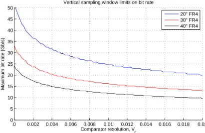
ωn = Tπ at the receiver.) The maximum data rate according to this constraint is shown in figure 1-5;
transmitter output swing is limited to a typical value of 400 mV.
The theoretical maximum bit rates computed by this simple model for PAM2 are lower than the bounds found in [23], but still higher than the data rates we are concerned with (10 Gb/s and below). Henceforth the effects of random noise will be ignored.
1.1.5 Crosstalk
Crosstalk is an undesired mixing between multiple channels, as shown in figure 1-6. Crosstalk causes BUJ because the disturbances often occur during transitions. It should be possible to cancel crosstalk by using parameterized analog filters to emulate and subtract out the undesired voltages [17]. However, the crosstalk
0 0.002 0.004 0.006 0.008 0.01 0.012 0.014 0.016 0.018 0.02 0 5 10 15 20 25 30 35 40 45 50 Comparator resolution, Vc
Maximum bit rate (Gb/s)
Vertical sampling window limits on bit rate
20" FR4 30" FR4 40" FR4
Figure 1-5: Noise-limited bit rates for a PAM2 link as a function of the comparator resolution Vc.
H H Die Channel/Package Crosstalk In A In B Circuitry
Figure 1-6: Block diagram of crosstalk between two channels.
cancellation systems reported so far have been highly application-specific (i.e. [22]). Inventing a general system for BUJ compensation is important but beyond the scope of this work.
1.2 Project summary
Finite channel bandwidth causes DDJ, which is a pervasive problem limiting serial link performance. Jitter compensation circuits reduce DDJ by introducing variable-width pulses into a bitstream before it is trans-mitted. A low-power integrated cell described below can be inserted into existing serial links, as shown in figure 1-7. The compensation scheme is based on the observation that channel transition delays can be estimated using the previously transmitted data.
Transmitter
Lossy Channel Data In
DDJ Compensation Feed-forward
Figure 1-7: A serial link with feedforward DDJ compensation.
Figure 1-8: Introducing a delay at the transmitter reduces the data-dependent difference in received transition delays. The uncompensated trace from figure 1-3 (light green) is shown for comparison.
introduces data-dependent delays in the transmitted signal. In figure 1-8, the transmitted transition for the upper trace has been delayed by about 25 ps. This brings its received transition time much closer to that of the lower trace. Such a delay is an example of feed-forward jitter compensation. The effect of applying these delays over many bit periods is visible in the eye diagrams in figure 1-9.
Existing equalization techniques used to address channel loss are explained in the remainder of this section. The concept of asynchronous jitter compensation is explained in chapter 2, and the design of a digitally-controlled compensation circuit is presented in chapter 3. Simulation results and a discussion of the implications of this work follow the design review.
0 0.5 1 1.5 2 2.5 3 x 10⁻¹⁰ −0.6 −0.4 −0.2 0 0.2 0.4 0.6 Time (s) Differential amplitude (V)
Hybrid Line Eye
0 0.5 1 1.5 2 2.5 3 x 10⁻¹⁰ −1 −0.8 −0.6 −0.4 −0.2 0 0.2 0.4 0.6 0.8 Time (s) Differential amplitude (V) DDJ Eye
Figure 1-9: Eye diagrams for uncompensated (left) and compensated (right) 40” FR4 channels at 6.25 Gb/s.
1.3 Amplitude equalization techniques
Equalization (EQ) filters are often used to reduce jitter by introducing a high-frequency boost that compen-sates for the lowpass characteristic of the channel. One simple EQ is an RC shelving filter that diminishes the low-frequency component of the transmitted signal by a fixed amount, perhaps 6 dB below 3 GHz. Another is an FIR filter that subtracts a delayed version of the signal.
1.3.1 Transmit equalization
Transmitter EQ (also known as amplitude pre-emphasis) diminishes the jitter contribution of the channel by introducing exaggerated transitions. The modified pulse shape partially cancels out the ISI of closely packed bits. A typical implementation is shown in figure 1-10. These EQ circuits consume power proportional to the amount of high-frequency boost. A transmitter that steers a 16 mA tail current to swing 400 mV across a doubly-terminated 50 Ω channel would require 32 mA to do so with 6 dB of high-frequency boost. Despite this requirement, FIR transmit EQs are popular in serial links due to their simplicity and effectiveness.
1.3.2 Receive equalization
EQ can also be performed on the receive side to improve the eye opening while consuming less power than transmitter pre-emphasis. Receive EQs are generally linear filters with adjustable frequency responses.
Main transmit driver Pre-emphasis driver Delay 1 UI In P In N EQ Control 50 Ω 50 Ω Vtt Out N Out P
Figure 1-10: Transmit pre-emphasis using a 1-tap FIR filter.
In P In N A = 1 Data Vtt 50 Ω 50 Ω 2R KR KR C C
In P In N A = 1 Data Vtt 50 Ω 50 Ω . . . Clk w1 w2 w3 wn x-1 x-2 x-3 x-n
Figure 1-12: A DFE receiver.
to the comparator is
H(s) = 1 + sKRC
1 + K + sKRC
This filter has a zero at s = −KRC1 and a pole at s = −KRC1+K. The DC swing of the signal is reduced
by a factor of 1
1+K; this de-emphasis can be compensated with an amplifier, although noise and interference
are also amplified. Nevertheless, receive EQs of varying complexity are ubiquitous. A more complex and powerful type of EQ is described below.
1.3.3 Decision feedback equalization
Decision-feedback equalization (DFE) is a receive EQ technique that dynamically adjusts the equalizer’s frequency response in order to emulate and subtract out ISI introduced by the channel [20]. A DFE circuit is sketched out in figure 1-12.
The weights wiare updated periodically based on error information (typically using the sign-sign LMS
algorithm). This circuit has the potential to dramatically reduce ISI, allowing proper data recovery when the unequalized eye is closed. However, the digital circuitry needed to update filter coefficients is complex; power consumption increases with the number of filter taps; proper adaptation requires a sufficiently exciting signal [21]; and a high-speed clock is required for the registers. These drawbacks motivate the use of simpler EQ techniques whenever possible.
The existence of a proper receive EQ cannot be assumed in applications where the ICs on each side of the link are not designed to cooperate with each other (as in modular networking equipment). Even if they
Delay Delay Delay 10 ps 5 ps 3 ps Clk Data Out x[0] x[-2] x[-3] x[-4] 0 1 1 0 1 0
Figure 1-13: DDJ compensation device designed by Jim Buckwalter.
are, time-domain compensation techniques may still provide a useful power savings.
1.4 Phase equalization techniques
The term “phase equalization” refers to an equalization technique that does not alter the amplitude of the transmitted signal. Useful phase equalization filters are not LTI systems. It will be helpful to review the existing technique for DDJ compensation before discussing how to improve it.
1.4.1 The Buckwalter scheme
Jim Buckwalter (while a student at Caltech) contributed the bulk of the existing efforts in time-domain jitter compensation, which he has called phase pre-emphasis or deterministic jitter equalization (DJE) [5]. His work is motivated by the observation that it may take less power to adjust the time placement of transitions, instead of increasing their effective amplitude. Buckwalter noticed that the transition delay introduced by a channel is strongly dependent on the most recent bits. His DJE scheme (shown in figure 1-13) includes a chain of N programmable delay lines, each of which can be bypassed by a multiplexer. The input bitstream is fed through registers that keep track of the last N + 1 bits. Each of the relevant bits (from bit 2 to bit N + 1) is XORed with the current bit (bit 0) in order to determine whether the corresponding delay line should be engaged. The delays are scaled to reflect the diminishing importance of bits transmitted in the past.
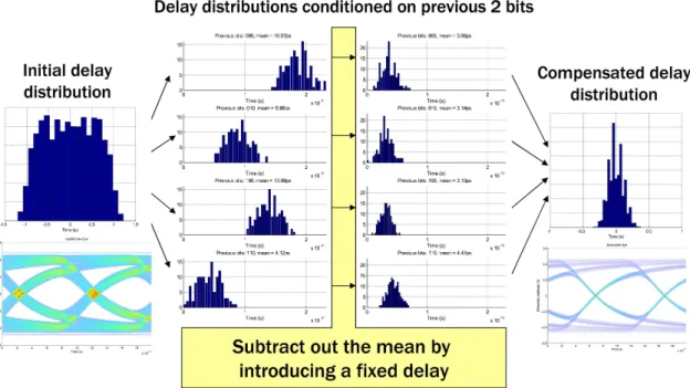
Figure 1-14: Jitter compensation viewed as an operation on jitter distributions.
1.4.2 Jitter histogram representation
Jitter can be interpreted as a probability distribution over transition delays. The goal of any jitter compensa-tion technique is to narrow the extents of this distribucompensa-tion. The peak-to-peak DDJ is much more important than the variance, because low error rates are needed and DDJ is not nearly Gaussian.
The Buckwalter scheme decomposes the distribution of transition delays into 2N narrower distributions,
each representing one possible combination of previous bits. The delay lines subtract out the mean from each conditional distribution. When those conditional distributions are added back together, the resulting delay distribution may be narrower than the original, indicating a reduction in jitter. This process is shown in figure 1-14. Increasing N increases the number of conditional distributions and improves the potential cancellation accuracy, at a cost of circuit complexity and power dissipation.
1.4.3 Reported performance results
The Buckwalter scheme has been employed in several published circuit designs. Table 1.1 summarizes the measured performance of those circuits.
We will see if similar results can be achieved using an asynchronous, analog approach to DDJ compen-sation. The goal is to come up with an improved tradeoff between jitter, vertical eye opening, and power consumption in a variety of link scenarios.
Jitter performance
Date Process Bit rate Before EQ After EQ PD Source
Oct. 2004 SiGe BiCMOS 10 Gb/s 35 mW [3]
Sep. 2005 0.13 µm CMOS 5 Gb/s 86 ps p-p 41.33 ps p-p 40 mW [4], [7] Sep. 2005 0.13 µm CMOS 10 Gb/s 50 ps p-p 35 ps p-p 40 mW [4], [7]
Jun. 2006 90 nm CMOS 6 Gb/s 16.15 ps RMS 10.29 ps RMS 6 mW [6] Table 1.1: Reported DDJ compensation circuit parameters and performance.
A DDJ Compensation Scheme
This chapter proposes an architecture for asynchronous DDJ compensation. Before examining the theory behind this architecture, let us define several variables of interest.
• xi: A sequence of bits, where each xi ∈ {0, 1}.
x0will be referred to as the current bit, whereas x−1, x−2, . . . are the previous bits.
• A: An alphabet of symbols mapping bit sequences to voltage values, e.g. A(0) = −1, A(1) = 1.
• xu(t): An uncompensated digital signal (the continuous-time version of xi) with uniform transition
times:
xu(t) =
∞ X i=−∞
A(xi) [u(t − iT ) − u(t − (i + 1)T )]
• h(t), H(jω): The impulse response and frequency response of the channel between the transmitter and receiver. The step response is s(t).
• di: A sequence of transition delays caused by the channel.
If xu(t) is transmitted, di is the difference between the ith bit transition times of xr(t) and xu(t).
Estimates of the delays are denoted by ˆdi.
• d(t): The transition delay caused by the channel (a continuous-time analog of di).
• xc(t): A digital signal with DDJ compensation applied to alter the transition times:
xc(t) = ∞ X i=−∞ A(xi) h
u(t − iT + ˆdi) − u(t − (i + 1)T + ˆdi+1) i
• xr(t): The received voltage signal:
xu(t) ∗ h(t) (without compensation)
xc(t) ∗ h(t) (with compensation)
The key to asynchronous DDJ compensation is maintaining a continuous-time estimate ˆd(t) of the
chan-nel’s transition delay for a transition at any given time. This delay is cancelled by a variable delay line placed
between xu(t) and xc(t).
2.1 Revisiting the Buckwalter scheme
The Buckwalter approach to jitter compensation is to introduce transition delays which are linearly depen-dent on the previous bits. These transition delays are controlled by digital logic. Two observations allow significant improvements to that approach:
1. A linear filter may be used to accumulate the appropriate delay for the entire history of the bitstream
with no additional power consumption.
2. The desired transition delay depends on the continuous-time history of the bitstream, so the system
can be run asynchronously. No clock or clock-recovery circuit is necessary.
In his thesis [5, p. 86], Buckwalter noticed a possibility: “Analog feedback could also be implemented without actually sampling the data to compensate the DDJ.” It is possible that he did not pursue the analog approach because of circuit implementation issues. We will attempt it here after developing a correspon-dence between the digital and analog methods.
2.1.1 Linear system interpretation
Buckwalter’s deterministic jitter equalizer (DJE) predicts transition delays using a discrete linear model. For
each incoming bit x0, the corresponding transition delay is estimated:
ˆ
d0 = d>(xi⊕ x0) + D
where d is a vector of delay coefficients and D is a constant propagation delay. The ⊕ symbol refers to an
XOR operation: the delays in d are introduced into xc(t) for each previous bit that differs from the current
0 1 2 3 4 5 6 7 8 9 10 11 0 2 4 6 8 10 12 14 Bit index Delay contribution (ps)
Discrete delay models of varying length
10 bits 4 bits 2 bits
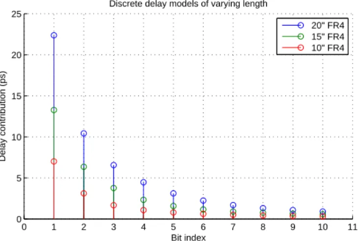
Figure 2-1: Delay coefficient vectors of varying length for a 15” FR4 channel at 10 Gb/s.
The coefficients in d can be estimated through SPICE transient simulations using a pseudorandom binary
sequence (PRBS) for xi. After thresholding xr(t), the sequence of delays dican be computed and regressed
against xi. The result of this operation is shown in figure 2-1. The indices i are plotted in reverse order;
coefficients shown farther to the right on the graph refer to bits farther in the past. The coefficients are independent of the model length. Implementing each coefficient requires additional circuitry, which is traded off against the diminishing returns in compensation accuracy.
The delay coefficients change when the channel’s frequency response changes. To model the frequency response of typical FR4 traces using SPICE simulation tools, a hybrid line model [18] splits the incident and reflected waves at each end and uses RLC ladders to approximate skin effect and dielectric loss. Figure 2-2 shows the delay coefficients for a few different channels represented by this model. The coefficients vary significantly, so all of the delay lines in a Buckwalter DJE need to be adjustable. (This can be accomplished by capacitively loaded inverters with an adjustable tail current.)
2.1.2 Interpolating delay coefficients
Figures 2-1 and 2-2 showed delay coefficients computed from a 10 Gb/s transient simulation. The estimated
transition delay is based on recent bits xi; given that A is linear, it is also a linear function of the
uncom-pensated voltage signal xu(t) at regularly spaced time intervals like xu(iT ), xu((i + 12)T ), etc. These
coefficients could conceivably be recomputed for different values of T , as the DDJ distribution varies with bit rate.
0 1 2 3 4 5 6 7 8 9 10 11 0 5 10 15 20 25 Bit index Delay contribution (ps)
Discrete delay models of varying length
20" FR4 15" FR4 10" FR4
Figure 2-2: Delay coefficients compared for 10”, 15”, and 20” long FR4 channels at 10 Gb/s.
the two functions:
y(t) = x(t) ∗ h(t) =
Z ∞
−∞
x(τ )h(t − τ )dτ
If xu(t) is an input and the transition delay of the channel (d(t)) is a desired output, then the delay
coefficients suggest the impulse response of the linear system that we need to calculate d(t). Our attention now shifts to computing this continuous-time function, along with a parameterized set of approximations that can be implemented using analog circuits.
2.2 Characteristic delay
The characteristic delay function defined here is a measure of the transition delay introduced into a digital bitstream by fixed-amplitude impulses in the past. It is a continuous-time coefficient vector for the linear model given above. The frequency response of a channel can be transformed into the characteristic delay, creating a useful abstraction for simulations and discussions of DDJ behavior.
In [11], Hajimiri et al. invoked a similar concept to explain the phase noise of oscillators in terms of their impulse sensitivity function (ISF). The ISF was defined as the phase deviation in an oscillator output due to an impulse at some input node. Unlike ISFs, characteristic delay functions are not periodic; they represent the sensitivity of a single transition time to the entire history of a bitstream. Also, the delay is not integrated over a series of transitions. Instead, the characteristic delay function models the channel’s
“memory” of previous transitions.
2.2.1 Definition
The characteristic delay of a PAM2 serial link is a function that can be convolved with a bitstream to obtain the transition delays d(t). Typical channels are symmetrical: rising and falling transitions behave identically.
This means that the transition delays on rising transitions (denoted by d+(t)) and falling transitions (d−(t))
can be computed using the same function. This function is the characteristic delay c(t), which satisfies
d+(t) = D − x(t) ∗ c(t)
d−(t) = D − x(t) ∗ c(t)
where x(t) is a digital signal at the input end of the channel and x(t) is its complement. From now on we
will refer to a single delay function d(t), which has the value of d+(t) when the current bit is 0 and d−(t)
when the current bit is 1.
The discrete series of transition delays imposed on a bitstream with clock period T is di = d(iT ). In a
DDJ compensator, we start with the uncompensated bitstream xu(t) and complement the estimated delays:
xc(t) = xu(t − (D − ˆd(t)))
If d(t) ≈ d(t + d(t)), then the transition delay estimate ˆd(t) can be computed accurately from the
uncom-pensated bitstream xu(t), even though the compensated bitstream xc(t) is the one seen by the channel. The
important implication for DDJ compensator design is that it is possible to run the compensator open-loop. The delay errors are mild when the delays are small relative to the decay time of the characteristic delay function.
2.2.2 Computation and fitting
In order to calculate the characteristic delay of a channel, assume that the transition delay is a linear function
of the transmitted signal.1 Also assume that there are only 2 possible symbols (“0” and “1”) and that a
threshold is placed halfway between the symbols without hysteresis. If a step in the input occurs at time t = 0, the threshold crossing time is D = s−1(1
2), where s(t) is the channel’s unit step response. When
an impulse at time −t is added to this input, the tail of the channel’s impulse response will bump up the 1This is not true, but we will show in section 2.4 that the nonlinearity is usually negligible.
108 109 1010 1011 −40 −35 −30 −25 −20 −15 −10 −5 0 5 Frequency (Hz) Channel frequency response
0 0.5 1 1.5 2 2.5 3 3.5 4 x 10⁻¹⁰ −0.01 0 0.01 0.02 0.03 0.04 Time (s) Channel impulse response
0 0.2 0.4 0.6 0.8 1 x 10⁻⁹ 0 0.2 0.4 0.6 0.8 1 1.2 1.4x 10 −10 Time (s) Delay (s)
Characteristic delay impulse response
108 109 1010 1011 −50 −40 −30 −20 −10 0 10 Frequency (Hz) Magnitude (dB)
Characteristic delay frequency response (referred to 100 ps)
5" FR4 10" FR4 15" FR4 20" FR4 30" FR4 40" FR4
Figure 2-3: Channel responses (left) and the corresponding characteristic delay responses (right); in the frequency domain (top) and time domain (bottom).
step portion of its output, reducing the transition delay to D − c(t). As the impulse recedes into the past
(t → ∞), its contribution to the transition delay will diminish: limt→∞c(t) = 0.
Within this space of stimulus signals, the function c(t) satisfies c(t) = s−1(1
2 − h(t + c(t)))
It can be computed numerically using a simple iterative algorithm:
c0(t) = 0
cn(t) = s−1(1
2 − h(t + cn−1(t)))
where, again, s−1(˙) is the inverse of the channel’s step response.
The characteristic delay depends only on the frequency response of the channel. Examples of the cor-respondence between frequency response and characteristic delay function are shown in figure 2-3. As the channel becomes longer, the characteristic delay becomes larger and is weighted to lower frequencies, indicating that a longer segment of the bitstream history is relevant to each transition delay.
0 1 2 3 4 5 x 10⁻¹⁰ 0 0.5 1 x 10⁻¹⁰ Time (s) Delay (s)
Characteristic delay impulse response: 10" channel Char. delay 2nd−order fit 1st−order fit 0 1 2 3 4 5 x 10⁻¹⁰ 0 0.5 1 x 10⁻¹⁰ Time (s) Delay (s)
Characteristic delay impulse response: 20" channel Char. delay 2nd−order fit 1st−order fit 0 1 2 3 4 5 x 10⁻¹⁰ 0 0.5 1 x 10⁻¹⁰ Time (s) Delay (s)
Characteristic delay impulse response: 30" channel Char. delay 2nd−order fit 1st−order fit
Figure 2-4: Characteristic delay functions for 10”, 20” and 30” FR4 channels. 1st- and 2nd-order fits to the impulse responses are also shown.
If represented as a voltage, the characteristic delay function is appropriate for controlling a voltage-controlled delay line operating on the bitstream. The characteristic delay function of an FR4 PCB trace appears to be well-approximated by a mixture of two exponential decays. Figure 2-4 demonstrates the use of RC filters to emulate the characteristic delay responses for a few common channel lengths.
2.3 Using a continuously variable delay line
The next challenge is to implement a transition delay proportional to the output of a characteristic delay emulator. If the sign of proportionality is positive, the delay line will introduce a jitter distribution similar to that of the channel. If the sign is negative, the jitter introduced by the delay line will cancel the jitter introduced by the channel.
Very accurate delay lines have been described in the literature, but the time needed to adjust the delay can be significant. In a DDJ compensator, the delay has to be adjusted within a single bit period. While several delay lines could be interleaved to avoid settling issues, it would be preferable to have a continuously variable delay line with a very fast adjustment capability.
Reset
Edge detector
Ramp generator Char. delay emulator
Comparator
xu(t)
xc(t)
r(t)
d(t) dh(t)
Figure 2-5: An architecture for asynchronous DDJ compensation.
2.3.1 Ramp-based implementation
One way to introduce delays in a digital signal is to limit its slew rate and threshold it again. This is the mechanism that causes propagation delays in digital circuits. The delays depend on the threshold voltage; offsetting the threshold causes duty-cycle distortion. Furthermore, a time-varying threshold can be used to provide a time-varying delay. If the slew rate is constant (as it is for a ramp signal), then the delay introduced is proportional to the difference between the threshold and input voltages. This technique can be used to generate very precisely adjustable delays [16].
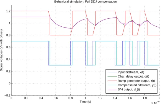
Figure 2-5 shows an architecture for DDJ compensation based on this concept. A characteristic delay
emulator (CDE) watches the transmitted signal xc(t) and produces the continuous-time delay estimate, ˆd(t).
When a transition arrives at time t0, this function sampled and held at dh(t) = ˆd(t0). The input bitstream
is fed into a slew rate limiter, or ramp generator. The output of this ramp generator r(t) is compared to the
delay control signal dh(t) in order to generate delayed transitions.
Figure 2-6 shows an idealized transient simulation demonstrating how this architecture generates the appropriate delays for DDJ compensation. The delay control signal follows the input bitstream. The desired
XOR function is accomplished because the comparator thresholds the difference dh(t) − r(t), where r(t)
0 0.2 0.4 0.6 0.8 1 1.2 1.4 1.6 1.8 2 x 10⁻⁹ −0.2 0 0.2 0.4 0.6 0.8 1 1.2 Time (s)
Signal voltages (V) with offsets
Behavioral simulation: Full DDJ compensation
Input bitstream, x(t) Char. delay output, d(t) Ramp generator output, r(t) Compensated bitstream, y(t) S/H output, dh(t)
Figure 2-6: Plots of voltage signals within ramp-based DDJ compensator.
2.3.2 Simplifications
Implementing a circuit using the architecture of figure 2-5 would be daunting because of the very fast feedback that it requires:
1. The rise times of the signals must be very short (perhaps 30-50 ps). This makes it difficult to detect
and act on edges.
2. The ramp generator has to be reset after each compensated transition in order to ensure that the delays
are consistent.
3. Propagation delay through the comparator must be considered in the design of the characteristic delay
emulator.
To avoid these complications, we try a simpler architecture (shown in figure 2-7) with the following modifications:
1. The ramp generator does not reset; instead, the output is clamped to a fixed range and the slew rate is
made fast enough to sweep across this entire range in one bit period.
2. The characteristic delay emulator is driven by the uncompensated signal instead of the compensated
Ramp generator Char. delay emulator
Comparator
xu(t) xc(t)
r(t)
d(t)
Figure 2-7: A simplified architecture for asynchronous DDJ compensation.
3. The output of the characteristic delay emulator is used as the delay control signal, and the
sample-and-hold circuit is eliminated.
The first change limits the amount of delay, and hence the peak-to-peak magnitude of DDJ that can be compensated, to less than one bit period. The second and third changes reduce compensation accuracy, but the damage is minor because the delay control signal varies much more slowly than the other signals. Despite the changes, the two architectures are very similar conceptually. A behavioral simulation of the simple architecture (figure 2-8) produces a compensated output signal that is almost exactly the same as the complete architecture (figure 2-6). These simplifications were essential for a lightweight implementation of the circuitry.
2.4 Nonlinear methods
If desired, a scalar nonlinear function of the bitstream could be implemented using the scheme shown in figure 2-9, where neither “system 1” nor “system 2” is an integrator. Figure 2-10 illustrates the idea of comparing the outputs of two different filters. It will be shown below that such a scheme is not necessary even though channel-induced transition delays are not a linear function of the data being transmitted.
The PAM2 transmitted signal xu(t) has no DC offset and a rising transition at t = 0. We are interested in
finding a way to anticipate and correct the transition delays d(t) between xu(t) and xr(t). The characteristic
delay has been proposed as a link between xu(t) and d(t), but it might be invalid because of a nonlinear or
time-varying correspondence.
Intuitively, there is no way that the transition delay could be linear for analog input signals because d(t) is subject to the nonlinear shape of the channel’s step response. What makes this problem much less obvious in context is the constant amplitude of digital signals, at least over the time intervals that matter for DDJ. We are only worried about adding signals of the same amplitude that contain pulses at different times. Even in
0 0.2 0.4 0.6 0.8 1 1.2 1.4 1.6 1.8 2 x 10⁻⁹ −0.2 0 0.2 0.4 0.6 0.8 1 1.2 Time (s)
Signal voltages (V) with offsets
Behavioral simulation: Simplified DDJ compensation
Input bitstream, x(t) Char. delay output, d(t) Ramp generator output, r(t) Compensated bitstream, y(t)
Figure 2-8: Plots of voltage signals within simplified DDJ compensator.
Comparator xu(t) xc(t) h1(t) h2(t) System 1 System 2
0 0.2 0.4 0.6 0.8 1 1.2 1.4 1.6 x 10⁻⁹ 0 0.2 0.4 0.6 0.8 1 1.2 1.4 Time (s)
Signal amplitudes (V) with offsets
Behavioral simulation: Nonlinear DDJ compensation
Uncompendated bitstream System 1 output System 2 output Compensated bitstream
Figure 2-10: Plots of voltage signals within nonlinear DDJ compensator.
this situation the delay is nonlinear, but the error introduced by a linear approximation to d(t) is acceptably small.
2.4.1 Nonlinearity in desired delays
Analytical example
Let the channel be a first-order lowpass filer: h(t) = e−τt. We will derive the linearity error analytically for
this channel and then compute it numerically for more realistic channel models.
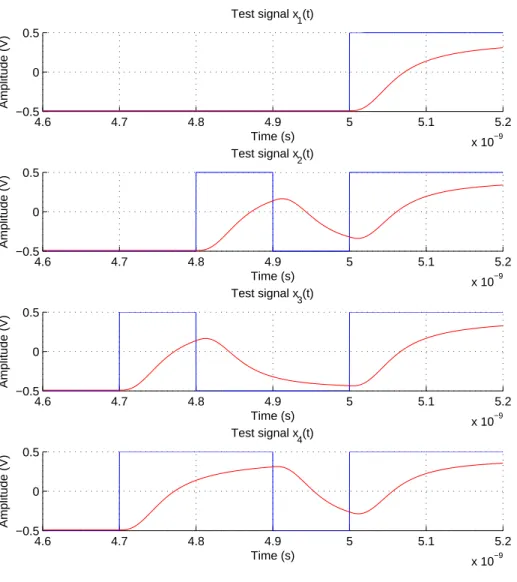
To test whether the first-order channel has a linear delay characteristic, try three different input histories:
xu1(t) = u(t + T1) − u(t + T2)
xu2(t) = u(t + T2) − u(t + T3)
xu3(t) = u(t + T1) − u(t + T3)
Enforce T1 > T2 > T3. This means xu1(t) and xu2(t) have non-overlapping pulses in the recent past,
and xu3(t) is their sum.
the state of the channel at t = 0−in each case: xr1(0−) = e− T2 τ − e−T1τ xr2(0−) = e− T3 τ − e−T2τ xr3(0−) = e− T3 τ − e−T1τ
The transition delay in question is d0. The threshold crossings occur when xr(t) = 12.
xr(d0) = 1 − £ 1 − xr(0−) ¤ e−d0τ = 1 2 £ 1 − xr(0−) ¤ e−d0τ = 1 2 d0 = τ ¡ ln 2 − ln£1 − xr(0−) ¤¢
The difference in delay time relative to the maximum of D = τ ln 2 is:
dr= D − d0
= τ ln£1 − xr(0−)¤
It should be clear from this expression that while xr(0) is a linear function of xu(t), the relative transition
delay is not. The exact relative delays are:
dr1 = τ ln h 1 − e−T2τ + e−T1τ i dr2 = τ ln h 1 − e−T3τ + e−T2τ i dr3 = τ ln h 1 − e−T3τ + e−T1τ i Numerical example
The three cases considered above were simulated with a 15” FR4 channel in addition to an RC filter. They are shown in figure 2-11 along with the step response. The delays are summarized in table 2.1.
If the transition delay were linear, then dr3 would equal dr2+dr1, corresponding to x3(t) = x2(t)+x1(t)
before the transition. The difference ∆t = dr3 − (dr2 + dr1) is the linearity error. The simulated error of
0.15 ps is quite small. This analysis shows that a linear estimator based on the characteristic delay may be very accurate.
4.6 4.7 4.8 4.9 5 5.1 5.2 x 10⁻⁹ −0.5 0 0.5 Time (s) Amplitude (V) Test signal x 1(t) 4.6 4.7 4.8 4.9 5 5.1 5.2 x 10⁻⁹ −0.5 0 0.5 Time (s) Amplitude (V) Test signal x 2(t) 4.6 4.7 4.8 4.9 5 5.1 5.2 x 10⁻⁹ −0.5 0 0.5 Time (s) Amplitude (V) Test signal x3(t) 4.6 4.7 4.8 4.9 5 5.1 5.2 x 10⁻⁹ −0.5 0 0.5 Time (s) Amplitude (V) Test signal x 4(t)
Case Signal Transition delay Relative delay
0 Step 71.8 ps 0 ps
1 Step + Pulse 1 61.2 ps −10.53 ps
2 Step + Pulse 2 66.5 ps −5.18 ps
3 Step + Both pulses 56.2 ps −15.56 ps
Add delays for cases 1 and 2 63.6 ps −15.71 ps Difference between expected and actual delays in case 3 −0.15 ps
Table 2.1: Results of simulating test cases using 15” FR4 channel.
It is conceivable that linearity errors could grow rapidly with DDJ magnitude. To compute an upper
bound on this error, we will simplify the expressions by imposing a uniform clock. Let xu1(t) have a pulse
two bit periods in the past, and let xu2(t) have a pulse three bit periods in the past. (The most recent bit must
be 0 in order to have a rising edge.) To apply these changes, substitute T1= 3T , T2= 2T , T3 = T into the
above formula. T only appears in exponents, so we can also let α = e−Tτ.
∆t = dr3− (dr2 + dr1) = τ ln 1 − e−T3τ + e−T1τ h 1 − e−T3τ + e−T2τ i h1 − e−T2τ + e−T1τ i = τ ln 1 − α + α 3 [1 − α + α2] [1 − α2+ α3] = τ ln 1 − α + α 3 1 − α + 2α3− 2α4+ α5 = τ ln · 1 − α3− 2α4+ α5 1 − α + 2α3− 2α4+ α5 ¸
The above result is exact for a first-order channel, but still complicated. Introducing the approximations ln(1 + x) ≈ x and α ¿ 1 (discarding higher order terms in α):
∆t ≈ − α3− 2α4+ α5 1 − α + 2α3− 2α4+ α5 ≈ − α3 1 − α = − e− 3T τ 1 − e−Tτ
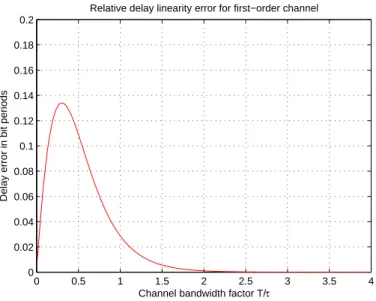
To help interpret this result, figure 2-12 shows the analytically computed error in unit intervals with
respect to Tτ, the ratio of the bit period to the channel time constant. The first-order approximation to a 15”
hybrid line model has a −3 dB point of 2 GHz and τ = 80 ps. At 10 Gb/s, Tτ = 1.26 (α = 0.28) and the
0 0.5 1 1.5 2 2.5 3 3.5 4 0 0.02 0.04 0.06 0.08 0.1 0.12 0.14 0.16 0.18 0.2
Relative delay linearity error for first−order channel
Channel bandwidth factor T/τ
Delay error in bit periods
Figure 2-12: Deviation from transition delay linearity for a first-order channel.
a numerical simulation of that channel (1.37 ps). The simulated linearity error for the hybrid line, 0.15 ps, is even smaller because of the inertial characteristics of the line.
Note that the errors can become large if the channel is grossly bandlimited (Tτ < 1). This is the regime
of operation that could benefit most from DDJ compensation. The error reaches 5% of a bit period at a relatively low channel bandwidth: −3 dB at 1.3 GHz (corresponding to a 20” FR4 trace) for 10 Gb/s data. Linear DDJ compensation is still useful in this case due to the large overall DDJ magnitude.
2.4.2 Mitigating linearity errors
The linearity error is always negative if the step response is monotonic. This means that a system designed to compensate jitter using a linear transition delay estimate will always overcompensate transitions that require a lot of delay. Passing the estimated delay through a nonlinear function could help, because the most negative error will be incurred for the largest relative delays.
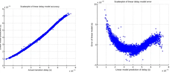
Figure 2-13 is a scatterplot of the exact versus approximated relative delays for a 25” long channel at 10 Gb/s. Note the positive curvature, indicating that edges expected to propagate down the channel more quickly are overcompensated. If a simple nonlinear function were applied to the delay, the general trend of the error could be flattened out. There is some variance in the actual delays; even an arbitrary pair of nonlinear systems (as in figure 2-9) could not eliminate all delay errors. Because of the recursive nature of the transition delay calculation, doing so would be akin to looking into the future.
0 1 2 3 4 5 6 7 8 x 10⁻¹¹ 0 1 2 3 4 5 6 7 8x 10
−11 Scatterplot of linear delay model accuracy
Actual transition delay (s)
Linear model prediction (s)
0 1 2 3 4 5 6 7 8 x 10⁻¹¹ −5 0 5 10x 10 −12
Linear model prediction of delay (s)
Error of linear model (s)
Scatterplot of linear delay model error
Figure 2-13: Scatter plots of the actual vs. predicted transition delays (left) and errors vs. predicted delays (right) for 25” FR4 channel at 10 Gb/s.
to implement an appropriate nonlinear CDE would likely result in diminishing returns, so we will defer them to future work.
2.5 Discussion
2.5.1 Compensating transmitter jitter
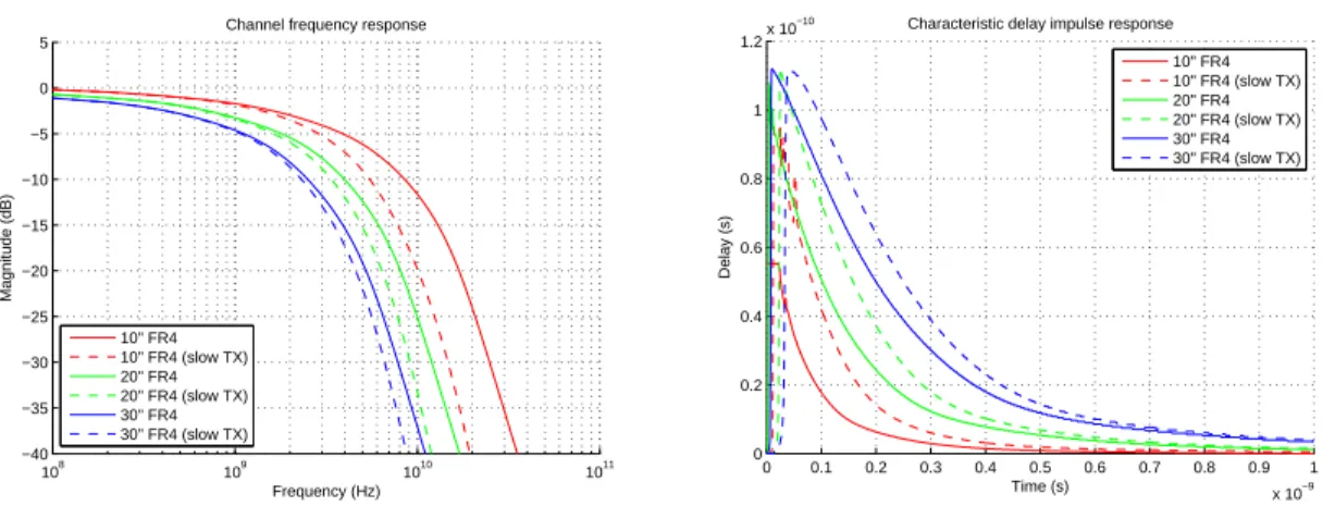
Investigations of DDJ in serial links led to some uncertainty over the exact meaning of “channel.” At mi-crowave frequencies the frequency response of the transmitter circuit, as well as the package parasitics, deviates noticeably from 1. Because the DDJ distribution caused by a channel depends on the frequency re-sponse, these components undoubtedly influence the received DDJ distribution. These effects are visible in the characteristic delay function. Figure 2-14 shows channel frequency responses and characteristic delays simulated with and without the addition of a second-order rolloff at 8 GHz.
In these simulations, the transmitter’s output settles much more quickly than the channel’s. This ex-plains why its effect on the characteristic delay is much more pronounced in the first few unit intervals. To compensate the additional DDJ caused by a bandlimited transmitter, the high-frequency component of the CDE response would need to be boosted. This may be a useful technique for increasing fanout ratios, reducing power consumption, or otherwise extending the useful bit rates of slower circuit technologies (e.g. 0.35 µm). To maintain some generality in the more detailed simulations that follow, the transmitter will be considered ideal.
108 109 1010 1011 −40 −35 −30 −25 −20 −15 −10 −5 0 5 Frequency (Hz) Magnitude (dB)
Channel frequency response
10" FR4 10" FR4 (slow TX) 20" FR4 20" FR4 (slow TX) 30" FR4 30" FR4 (slow TX) 0 0.1 0.2 0.3 0.4 0.5 0.6 0.7 0.8 0.9 1 x 10⁻⁹ 0 0.2 0.4 0.6 0.8 1 1.2x 10 Time (s) Delay (s)
Characteristic delay impulse response 10" FR4 10" FR4 (slow TX) 20" FR4 20" FR4 (slow TX) 30" FR4 30" FR4 (slow TX)
Figure 2-14: Frequency responses and characteristic delay functions for FR4 channels modeled with and without the effects of finite transmitter bandwidth.
The quality of compensation is limited by the complexity of the filters used in the emulator.
2.5.2 Summary
This chapter defined the characteristic delay function, a property of the channel which can be computed from the channel’s frequency response. The characteristic delay function is the coefficient vector in a continuous-time linear model of transition delays. An architecture for DDJ compensation based on this model was presented. After observing several circuit design challenges, the architecture was simplified at some cost in theoretical compensation accuracy. Concerns about the inherent nonlinearity of DDJ motivated a more care-ful examination of the validity of the linear transition delay model. Analytical and numerical experiments quantified the expected compensation errors. Since those errors are acceptably small, we are prepared to proceed in implementing the compensator.
Design Review
3.1 Top-level overview
A circuit block ddj comp, designed for a 0.35µm BiCMOS process, performs asynchronous jitter com-pensation in a serial transmitter using the simplified architecture shown in figure 2-7. Its schematic is shown in figure 3-1. A differential input bitstream (ip, in) with approximately 200 mV swing is passed through an adjustable ramp generator and an adjustable CDE. The differential outputs of these two subcircuits are compared to produce a compensated bitstream (op, on). Two auxiliary subcircuits have been added to the basic architecture: a small delay cell placed in front of the CDE, and an adjustable current mirror for a set of current sources that track the delay sensitivity.
The following sections review the design of each subcircuit, explaining the tradeoffs that were needed to achieve effective compensation at 6 Gb/s and above despite the relatively slow process technology. NPN bipolar transistors have been used throughout the signal path because the other active devices are not fast enough.
The design assumes the existence of a 0.1 mA reference current into the drain of a 10 µm × 1 µm MOSFET. Current sinks driven from the bias line in the following schematics draw approximately 10 µA per unit WL.
3.2 Adjustment mechanisms
As described in section 2.1.1, the characteristic delay function depends on the frequency response of the channel. While there is an infinite-dimensional space of possible frequency responses, most channels en-countered in wireline applications share similar frequency response characteristics (see section 1.1.2). For
Slow LP
Fast LP CM out
Bias Ramp Clamp
CM out CMFB in Ramp Clamp cd_mag_fast cd_mag_slow ramp_speed bias ip in op on Adjustable current mirror 40ps delay cell CMFB Comparator Characteristic delay emulator generator Ramp Vref
Figure 3-1: Top-level schematic of DDJ compensator.
copper traces on FR4 circuit boards, the characteristic delay function can be approximated by a sum of first-order lowpass filters. To simplify the circuitry even more, these lowpass filters have fixed corner frequencies; only their amplitudes are adjustable.
Remember that the ramp generator and comparator constitute a continuously variable delay line. The slew rate of the ramp generator output controls the sensitivity of this delay line. (If ramp generator had infinite slew rate, then the CDE output would be compared to a square wave, and no delay would be intro-duced on any transition.) Slower slew rates lead to larger delays, which are useful for compensating lossier channels.
The two CDE adjustments and one ramp generator adjustment are each represented by a 3-bit binary code. They are referred to as:
1. cd mag slow[2:0]: Voltage swing of the low-frequency component of the CDE output
2. cd mag slow[2:0]: Voltage swing of the high-frequency component of the CDE output
3. ramp speed[2:0]: Slew rate of the ramp generator
Table 3.1 provides a rough guide for setting these digital codes based on the bit rate and channel length. As the channel gets longer, the overall amount of compensation should be increased and the CDE output
Situation Optimal settings
Bit rate Trace length ramp speed cd mag fast cd mag slow
6.25 Gb/s 20” 5 2 1 6.25 Gb/s 30” 5 3 3 6.25 Gb/s 40” 5 5 7 10 Gb/s 15” 7 0 0 10 Gb/s 20” 7 1 1 10 Gb/s 25” 7 4 2
Table 3.1: Optimal settings for digital controls of DDJ compensator in nominal process conditions.
should be weighted towards low frequencies (matching the trend in characteristic delay shown in figure 2-3). This guide is based on simulation results; in a complete IC implementation, the adjustment settings will be stored in registers. They should be adjusted in their final application circuit with the aid of test equipment to minimize received jitter.
3.3 Characteristic delay emulator (CDE)
The CDE is a circuit providing a mixture of two first-order filters, as shown in figure 3-2. To fix the signal amplitudes at levels determined by the cd mag slow and cd mag fast settings, the input bitstream is first passed through two variable-amplitude limiters. The output of each limiter is individually filtered, then
the outputs are summed. The resulting differential voltage is Vout:
h1(t) = e− t R1C1 h2(t) = e− t R2C2 Vout= V0[A1sgn Vin(t) ∗ h1(t) + A2 sgn Vin(t) ∗ h2(t)]
3.3.1 Variable amplitude input limiter
The CDE’s input limiter arrangement is shown in figure 3-3. Each of the magnitude control codes is con-nected to a simple NMOS current DAC. The output swing of the limiter is the variable bias current multiplied by the fixed resistive load. Each DAC sinks between 20 to 160 µA. The load resistors are 900 Ω, resulting in ±18 to ±144 mV swing from each limiter.
1 1 Vin Vout A1 A2 R1 C1 R2 C2 V0 V0
Figure 3-2: Concept of CDE filters.
CMFB In P In N Out 1 Out 2 Amplitude 1 Amplitude 2 1 1 CMFB RL I1 I2 RL RL RL Vref Iout Iout