Publisher’s version / Version de l'éditeur:
Vous avez des questions? Nous pouvons vous aider. Pour communiquer directement avec un auteur, consultez la première page de la revue dans laquelle son article a été publié afin de trouver ses coordonnées. Si vous n’arrivez pas à les repérer, communiquez avec nous à PublicationsArchive-ArchivesPublications@nrc-cnrc.gc.ca.
Questions? Contact the NRC Publications Archive team at
PublicationsArchive-ArchivesPublications@nrc-cnrc.gc.ca. If you wish to email the authors directly, please see the first page of the publication for their contact information.
https://publications-cnrc.canada.ca/fra/droits
L’accès à ce site Web et l’utilisation de son contenu sont assujettis aux conditions présentées dans le site LISEZ CES CONDITIONS ATTENTIVEMENT AVANT D’UTILISER CE SITE WEB.
Physical Review. B, Condensed Matter and Materials Physics, 81, 23, p. 235426,
2010-05-24
READ THESE TERMS AND CONDITIONS CAREFULLY BEFORE USING THIS WEBSITE. https://nrc-publications.canada.ca/eng/copyright
NRC Publications Archive Record / Notice des Archives des publications du CNRC :
https://nrc-publications.canada.ca/eng/view/object/?id=69ef1221-55a3-4b02-83cc-496e5cc0936e
https://publications-cnrc.canada.ca/fra/voir/objet/?id=69ef1221-55a3-4b02-83cc-496e5cc0936e
NRC Publications Archive
Archives des publications du CNRC
This publication could be one of several versions: author’s original, accepted manuscript or the publisher’s version. / La version de cette publication peut être l’une des suivantes : la version prépublication de l’auteur, la version acceptée du manuscrit ou la version de l’éditeur.
For the publisher’s version, please access the DOI link below./ Pour consulter la version de l’éditeur, utilisez le lien DOI ci-dessous.
https://doi.org/10.1103/PhysRevB.81.235426
Access and use of this website and the material on it are subject to the Terms and Conditions set forth at
Carrier thermal escape in families of InAs/InP self-assembled quantum
dots
Gélinas, Guillaume; Lanacer, Ali; Leonelli, Richard; Masut, Remo A.; Poole,
Philip J.
Carrier thermal escape in families of InAs/InP self-assembled quantum dots
Guillaume Gélinas, Ali Lanacer, and Richard Leonelli
*
Département de Physique and Regroupement Québécois sur les Matériaux de Pointe (RQMP), Université de Montréal, Case Postale 6128, Succursale Centre-ville, Montréal, Québec, Canada H3C 3J7
Remo A. Masut
Département de Génie Physique and Regroupement Québécois sur les matériaux de pointe (RQMP), École Polytechnique, Case Postale 6079, Succursale Centre-ville, Montréal, Québec, Canada H3C 3A7
Philip J. Poole
Institute for Microstructural Sciences, National Research Council of Canada, 1200 Montreal Road, Ottawa, Ontario, Canada K1A 0R6
共Received 15 October 2009; revised manuscript received 24 May 2010; published 18 June 2010兲
The temperature evolution of the photoluminescence spectra of two samples of single-layer InAs/InP共001兲 self-assembled quantum dots is measured from 10 to 300 K. To understand the thermal quenching of their multimodal emission, we develop a coupled rate-equation model that includes the effect of carrier thermal escape from a quantum dot to the wetting layer and to the InP matrix, followed by transport, recapture or nonradiative recombination. Our model reproduces the temperature dependence of the emission of each family of quantum dots with a single set of parameters. We find that the main escape mechanism of the carriers confined in the quantum dots is through thermal emission to the wetting layer. The activation energy for this process is found to be close to one half the energy difference between that of a given family of quantum dots and that of the wetting layer as measured by photoluminescence excitation experiments. This indicates that electron and holes exit the InAs quantum dots as correlated pairs.
DOI:10.1103/PhysRevB.81.235426 PACS number共s兲: 78.67.Hc, 78.55.Cr
I. INTRODUCTION
Quantum dots 共QDs兲 are designable mesoscopic atomic assemblies whose effective electronic density of states is ␦ functionlike.1 One of the most studied systems is
self-assembled QDs grown in the Stransky-Krastanow mode. It has been demonstrated that self-assembled QDs can find ap-plications in fields ranging from nano-optoelectronics2 to
quantum computing.3Understanding the processes that result
in the thermal quenching of the photoluminescence 共PL兲 of QDs is thus important not only on fundamental grounds but also for the realization of efficient devices operating at room temperature.
In the case of InAs/GaAs QDs, it is now well established that the two mechanisms that control the populations of electron-hole pairs in the ground state of QDs are their ra-diative recombination and their escape to higher-lying energy states. Thermal quenching then results from nonradiative re-combination processes that occur in one or several of those higher-energy states.4–16 Even though both measurements
and theoretical modeling appear straightforward, there re-mains to this day significant differences and apparent contra-dictions in the interpretation of the results published by dif-ferent groups over the last decade.
Two important questions remain unanswered. First, the identification of the higher-energy states that contain nonra-diative centers. Potential candidates are共i兲 the so-called wet-ting layer共WL兲, which is a few monolayer 共ML兲 thick InAs pseudomorphic quantum well 共QW兲 always present in the Stranski-Krastanow growth mode; 共ii兲 the matrix in which the QDs are inserted, either GaAs or a confining QW; 共iii兲 defects or impurities in the matrix; or共iv兲 QD excited states. Second, it is still not clear whether the confined electrons and holes escape a QD as a single quasiparticle 共exciton兲 or as
independent carriers. The nature of the escape mechanism can be revealed indirectly by the ratio
= Ei a/
⌬Ei, 共1兲
where Ei a
is the measured thermal activation energy and ⌬Ei
is the optical gap between the emission from the higher-energy state i and that of the QDs. In the case of exciton escape, Ei
a
= ⌬Eiand= 1. If single carrier escape dominates,
Eia corresponds to the confinement energy of the less con-fined carrier and ⬍ 1 / 2. Yang et al.4 pointed to another
possibility: that of a correlated e-h pair escape. No detailed correlation mechanism was proposed but it could arise, for example, if the escape of one of the carriers changes the potential landscape enough to induce dynamically the escape of the second one. As electrons and holes would then be, in average, emitted in pairs, their concentrations would be equal and thus determined by only half the optical gap en-ergy ⌬Ei. It follows that, in the case of a correlated pair
escape,= 1 / 2.
Carrier capture and recombination in QDs are random processes that require a master equation formalism in order to properly describe QD excited state dynamics.17–20
How-ever, under continuous-wave, low excitation conditions where the average number of electron-hole pairs per QD is much smaller than one, the predictions of more conventional and simple rate-equation models remain valid. Further, QD-size fluctuations result in a distribution of their quantized energies and hence to a distribution of activation energies. As temperature is increased, redistribution of the carrier popula-tion occurs toward the low-energy tail of the QD energy distribution.4–6,9,11 When the full width at half maximum
共FWHM兲 of the emission of the ensemble of QDs is much smaller than any expected activation energy, the QD energy
distribution is often represented by a␦function. The solution of the thermal rate equations in steady state for the ensemble PL intensity I then gives
I共T兲 = I0
冉
1 +兺
i=1 m Aie−Ei a/kT冊
−1 , 共2兲where m is the number of high-energy states involved and Eia is the activation energy for the transfer from QD to state i.12 Using this approach, Heitz et al.5pointed to transitions from
the ground-state exciton to QD excited states and to the WL while Le Ru et al.7 identified the GaAs matrix as the
domi-nant recombination state and obtained = 1. Using samples where the QDs were imbedded in an InGaAs QW, Torchys-nka et al.12,14 found several activation energies that
corre-sponded well to transitions from QDs to QW and from QW to the GaAs matrix, assuming= 1. Schulz et al. reported on InP QDs embedded in 共AlxGa1−x兲0.51In0.49P with a bimodal
height distribution. They found that the activation energy of the smaller dots corresponded to exciton escape while that of the larger dots was compatible with correlated pair escape.15
Seravalli et al. examined samples where the QDs were in-serted in InxGa1−xAs and In1−yAlyAs confining layers. They
found two dominant activation energies that corresponded to exciton transitions from QDs to an unidentified low-energy defect and transitions from QDs to the WL.16
More information is available if the internal population redistribution is also measured and modeled. In that case, the rate equations must take into account the QD energy distri-bution. Yang et al.4 analyzed the PL decay times within the
QD emission band with a model that only included the WL as the high-energy state. They found good agreement with experimental data with ⬇1/2. However, the validity their rate-equation model under pulsed excitation conditions is questionable.19 Sanguinetti et al.6 developed a model that
included exciton transitions from QDs to WL and WL to the GaAs matrix. It reproduced well the QD PL integrated inten-sity, FWHM, and peak energy as a function of temperature. Akiba et al.8studied InAs QDs in GaAs layers with a
trimo-dal height distribution. Their model, which assumed corre-lated pair escape, reproduced qualitatively the PL integrated intensity of the individual QD families as well as that of the WL. Dawson et al.9,11 included in their model independent
distributions of electrons and holes but they only considered transitions from QDs to the GaAs matrix. They found that the PL integrated intensity, FWHM, and peak energy was best fitted by uncorrelated carrier escape.
The reason for these discrepancies is unclear. One might point out different escape mechanisms in different samples, insufficient information provided by a single QD emission band, or differences in the theoretical models and/or assump-tions underlying their treatment. On the other hand, little work of a similar nature has been carried out on equivalent QDs grown on materials systems with an energy spectrum quantitatively different from that of InAs/GaAs. In order to solve some of the problems mentioned above, we present a study of the thermal quenching from two samples that con-tain a single layer of InAs QDs embedded in an InP matrix. Their PL spectra show several well-resolved emission bands,
extending from 0.75 to 1.1 eV, that can be associated with families of QDs that differ in height by 1 ML,21–28 while
their PL excitation 共PLE兲 spectra reveal absorption edges that we associate with QD excited states and WL resonances. The evolution with temperature of the multimodal PL of our samples imposes stringent constraints on a model based on coupled rate equations as it should reproduce the thermal behavior of many peaks with the same set of parameters.
II. EXPERIMENTAL PROCEDURES
Sample A was grown by low-pressure metal-organic vapor-phase epitaxy on 共001兲 InP Fe-doped semi-insulating substrates at a reactor pressure of 160 torr. Trimethylindium 共TMI兲, tertiarybutylarsine 共TBA兲, and tertiarybutylphosphine 共TBP兲 were used as precursors and Pd-purified H2 as the
carrier gas. The flow rates of TMI and TBA were kept at 0.05 and 0.95 mol s−1and the TBP flow rate was 3.5 mol s−1. After the growth at 600 ° C of a 100 nm InP buffer layer, the temperature was lowered to 500 ° C during 90 s while still growing InP. 2.4 InAs MLs, sandwiched between two 20-ML-thick InP layers, were then deposited at 500 ° C. The temperature was raised back to 600 ° C and the growth ter-minated by the deposition of a 30 nm InP cap layer. The growth interruption sequence used to switch from InP to InAs and back is described in Ref. 29. In particular, a 4 s growth interruption was applied after InAs deposition.
Sample B was grown on 共001兲 InP substrates by chemical-beam epitaxy from TMI, arsine 共AsH3兲, and
phos-phine共PH3兲. AsH3and PH3were cracked at 850 ° C in a fast
switching high-temperature injector to produce predomi-nantly As2and P2. After desorption of the surface oxide, the
growth was initiated with an InP buffer layer. Then, TMI and As2 were injected simultaneously into the chamber to grow
about 2.2 MLs of InAs layer at 515 ° C. This was followed by a 30 s growth interruption under an overpressure of As2to
allow the QDs to form. The QDs were then capped with InP. Further information on the growth procedure can be found in Ref. 28.
The PL measurements were carried out with the samples mounted strain free in a helium-flow cryostat. The excitation source was the weakly focused 632.8 nm line of a He-Ne laser. The excitation intensity was kept well below the satu-ration threshold of the QDs. The signal was analyzed with a spectrally calibrated, nitrogen-purged Fourier-transform spectrometer using a liquid-nitrogen-cooled InSb detector. The PLE was excited with the monochromatized light of a 150 W tungsten lamp. The PL was then analyzed with a 0.5 m double-grating spectrometer and detected with a liquid-nitrogen-cooled InGaAs photodetector array sensitive up to 2 m.
III. RESULTS
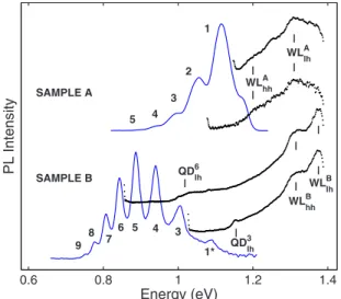
Figure 1shows the low-temperature PL and PLE spectra of the samples. The emission of sample A comprises five peaks while that of sample B comprises nine peaks. The energy position of peak B1ⴱencompasses those of peaks A1
GÉLINAS et al. PHYSICAL REVIEW B 81, 235426共2010兲
and A2 while the positions of peaks B3–B5 are close to those of peaks A3–A5.
The PLE spectra of peaks A1 and A2 are similar to what was previously reported in thin InAs QWs.27,30 They show
an edge at 1.19⫾ 0.01 eV and a resonance at 1.31⫾ 0.01 eV that correspond, respectively, to the electron to heavy- and light-hole transitions in a 2-ML-thick InAs/InP QW as cal-culated with the tight-binding method.27,31It follows that the high-energy tail of the emission from sample A at low tem-perature corresponds to residual emission from the WL.
The PLE spectra of peaks B3 and B6 are also shown in Fig.1. Two low-energy edges are observed, respectively, 150 meV 共B3兲 and 170 meV 共B6兲 above the emission peaks. They correspond to the first excited state QDlh. Two other
resonances appear at the same energies of 1.30⫾ 0.01 eV and 1.37⫾ 0.01 eV in both spectra. These are close to the expected transitions of a 1-ML InAs/InP QW. They can thus be attributed to the WLhhand WLlh transitions in sample B.
We attribute the fact that the WL is thinner in sample B than in sample A to the longer interruption that took place during the growth of sample B. This probably allowed the formation of thicker QDs at the expense of the WL. The difference in energy of the fundamental WL optical transition is useful for our purpose as it adds another constraint to the thermal model described in Sec.IV.
The evolution of the PL spectra of both samples as a function of temperature is depicted in Fig. 2. The emission from peak A1 is rapidly quenched for T ⬎ 100 K while that of peak A2 remains nearly constant for T ⬍ 170 K. The in-tensity of peaks A3–A5 actually increases for T⬃200 K be-fore decreasing at higher temperatures. The emission from sample B is more robust as only peaks B1ⴱ and B3 show a
significant intensity decrease at 300 K. No emission from QD excited states can be detected even at high temperatures.
IV. RATE-EQUATION MODEL
Our thermal model, which is schematized in Fig. 3, is similar to those developed in Refs. 4 and 6. A series of
coupled steady-state rate equations that control the popula-tions niin each state i is obtained from the detailed balance
principle,4 − ni
冉
Ri+兺
j⫽i NjUij冊
+ Ni兺
j⫽i njUji+ Pi= 0, 共3a兲where Ri is the recombination rate of state i, Nithe number
of states per unit area, and Uijthe transfer cross section from
state i to state j. Pi represents the carrier generation, i is
defined in Eq.共1兲 and
Uji= Uijexp
再
j共Ej− Ei兲
kT
冎
if Ej⬍ Ei. 共3b兲 We improved on previous models by incorporating sev-eral unique features.共i兲 Transfer from QDs to WL, from QDs to the InP matrix, and from WL to the InP matrix are al-lowed. 共ii兲 The allowed states of the WL and the InP matrix0.6 0.8 1 1.2 1.4 Energy (eV) PL Intensity SAMPLE A SAMPLE B WL hh A | | WL lh A | | 1 2 3 4 5 1* 3 4 5 6 7 8 9 QD lh 6 | WL hh B | | WL lh B | | QD lh 3 |
FIG. 1. 共Color online兲 Low-temperature PL and PLE spectra of samples A and B. QDlh, WLhh, WLlh, and InP refer to excitonic heavy- and light-hole resonances in QDs, WL, and the InP matrix, respectively. 0.7 0.8 0.9 1 1.1 1.2 Energy (eV) PL Intensity SAMPLE A SAMPLE B 50 K 100 150 200 250 50 K 100 150 200 250
FIG. 2. Evolution of the PL spectra of samples A and B as a function of temperature.
are distributed over a wide range of energy above their fun-damental edge, Eg
W
for the WL and Eg M
for InP. To make this fact numerically tractable, the WL is separated into segments of width ⌬EWextending from Eg
W
to Eg M
. The effective num-ber of states per unit area of each segment is NW= DW⌬EW,
where DW= mX
InAs/
ប2 is the two-dimensional density of
states in the WL. The InP matrix is similarly segmented. We assume a
冑
E− Eg dependence for its three-dimensionalden-sity of states. The number of states per unit area for a seg-ment that extends from Ei
min to Ei min + ⌬EMis thus NMi= 2 3DMᐉM关共Ei min + ⌬EM− Eg M兲3/2 −共Ei min − Eg M兲3/2兴, 共4兲 where DM= 21/2共mX InP兲3/2/共2ប3兲 共Ref.
32兲 and ᐉM is the
ac-tive thickness of the matrix. 共iii兲 Eg
W共T兲 and E g
M共T兲 are assumed to follow the Varshni
temperature dependence with the parameters of bulk InAs and InP, respectively.33
In order to restrain the number of adjustable parameters, the following assumptions were made:
Ri=
冦
RD if i 苸 D,
RW for W lowest energy segment,
RM for M lowest energy segment, 0 for all other states,
冧
共5a兲
i=
再
D if i 苸 D,
1 if i 苸 W,
冎
共5b兲Pi=
再
P if i = M highest energy segment,
0 if not,
冎
共5c兲 Uij=冦
0 if i and j 苸 D, UWD if i 苸 W and j 苸 D, UMD if i 苸 M and j 苸 D, UMW if i 苸 M and j 苸 W, UWW if i and j 苸 W, UMM if i and j 苸 M ,冧
共5d兲where D, W, and M refer, respectively, to the ensemble of QD, WL, and InP matrix states. We further assumed that the parameters in Eqs. 共5兲 are independent of temperature.
In Eq. 共5a兲, RDcorresponds to the QD radiative rate. As
no emission from the WL nor the InP matrix is observed at high temperature, RW and RM correspond to nonradiative
rates. RW was assigned only to the lowest-energy segment
because, in a QW, free excitons form two-dimensional po-laritons that do not couple to photonlike popo-laritons propagat-ing perpendicular to the QW plane unless their energy is within a small bandwidth near the bottom of the band.34
Excitons must thus relax to the bottom of their energy band before they can recombine radiatively or nonradiatively.35A
similar argument can be made for RM.36
QD excited states are sometimes reported in the high-temperature PL from InAs/GaAs QDs.5,14 In such a case,
they should be included in the thermal model within an ap-propriate formalism. In our case however, no excited state emission is detected. Further, the energy difference between QD first excited state and ground state is higher than 150 meV, about twice as much than what is observed in typical InAs/GaAs QDs.5 Thus, for our samples, the excited state
population remains small at all temperatures and their effect on thermal quenching can be neglected.
V. DISCUSSION
To compare the simulations with the experiments, the data were treated as follows. The peak energy and integrated in-tensity of each peak at a given temperature was obtained by fitting the PL spectrum with a series of Gaussian peaks. This procedure was found to reproduce well the PL spectra except for peak B1ⴱ. Its peak energy and intensity was obtained by
subtracting the intensity of all the other peaks from the total intensity of the PL emission. The energy position of each family of QDs served as input to the model.
In the model, the total number of QD states per unit area ND and the QD recombination rate RD are scaling factors.
The relative number of states for each QD family was as-sumed to be given by the relative intensity of the PL at low temperature. ⌬EWand ⌬EMwere set at 10 meV, a value close
to the spectral extent of the WL and InP matrix absorption edges. In Eq.共5d兲, the parameters UWWand UMMwere set to
a high value to ensure that the excitons in the WL and the InP matrix are in thermal equilibrium. Finally, we fixed ᐉMat
100 nm, a value close to the penetration length of the exci-tation source.37The model is thus left with seven adjustable materials parameters: RW/RD, RM/RD, UWDND/RD,
UMDND/RD, UMW,D, and Eg W共0兲.
The result of our simulations is presented in Fig.4and the optimized parameters are listed in Table I. The uncertainties ⌬ai of the optimized parameters were estimated using38
⌬ai=
冉
1 2 22 2ai冊
−1/2 . 共6兲Strictly speaking, Eq. 共6兲 is only valid if the cross-partial
derivatives2/a
iajare small with respect to the diagonal
terms, which is not the case here. However, it gives a good estimate of the sensitivity of the fit to a given parameter.
The temperature dependence of all peaks from sample A are very well reproduced by our model. In particular, it re-produces the intensity increase in peaks A3–A5 when T ⲏ 180 K. The fluctuations at high temperatures in the simu-lated curves are caused by the fluctuations in the energy po-sitions of the QD families, which are inserted in the model for each temperature. The fitted value for Eg
W共0兲 corresponds
within uncertainties to the measured value of the low-energy edge WLhh shown in Fig. 1. There is globally much less
thermal quenching in sample B and thus less dynamics to constrain the model. To extract relevant information, we fixed Eg
W共0兲 to the value of WL
hh obtained from the PLE
spectra of sample B shown in Fig.1. Here also, peaks B1ⴱ,
B3, and B4 are well reproduced by our simulations. There was nearly no change in intensity for peaks B5–B9 while our model predicts a slight increase. The discrepancy can easily
GÉLINAS et al. PHYSICAL REVIEW B 81, 235426共2010兲
be explained by the neglect of the temperature dependence of the parameters of the model.
It can be seen from TableIthat the parameters with high uncertainties are related to the InP matrix, an indication that for QDs, the main carrier escape and recapture channels are through the wetting layer. To further test this hypothesis, we deactivated the contribution to the thermal quenching of the InP matrix by fixing RM= 0. To reduce further the number of
adjustable parameters, Eg
W共0兲 was fixed at the value of WL hh
for each sample. In the case of sample A, no significant change in the fits was detected when using the remaining set of five parameters. However, a further reduction in the num-ber of parameters resulted in degraded fits. In particular, nei-ther UMDnor UMWcould be separately set to zero. Thus, our
model requires that the carriers injected in the matrix be captured both by the dots and the WL. In the case of sample B, the matrix could be entirely removed from the model and the experimental data fitted with only three variable
param-eters. This shows that, for our samples, the thermal quench-ing occurs through carrier escape from QD to WL followed by a nonradiative recombination of the carriers in the WL.
As for the parameter D, the simulations show that it is
close to one half for our samples. As Dis the most critical
parameter in our model, this indicates that electrons and holes escape from the QDs mostly as correlated e-h pairs. We thus corroborate the findings of Yang et al.4This is by no
means a trivial result as there are no compelling reason for the escape mechanism to involve correlated e-h pairs rather than uncorrelated pairs or excitons.
It is instructive to simulate with our model the tempera-ture dependence of the integrated intensity of a monomodal QD emission. We have generated a Gaussian distribution of 15 QD subfamilies centered at an energy EDand shifted with
respect to the WL by ⌬E = Eg W
− ED. The FWHM of the dis-tribution was fixed at 0.25⌬E, a value typical of monomodal InAs/GaAs QD emission.7 We used in the simulations the
same materials parameters as those found for sample A ex-cept for D= 0.5.
The result of our simulations for ⌬E = 100, 200, and 300 meV is shown as symbols in Fig. 5. The curves were ana-lyzed with a sum of activated processes as described by Eq.
0 5 10 15 20 10−2 10−1 100 101 102 103 104 105 1000/T (K−1) PL Intensity (arb. units ) A1 B1* A2 A3 B3 A4 B4 A5 B5
FIG. 4. 共Color online兲 Arrhenius plot of the temperature depen-dence of the integrated intensity of the individual families of QD’s. Labels A and B identify peaks from samples A and B, respectively. The curves have been shifted vertically for clarity.
TABLE I. Parameters obtained by fitting the model to the experimental data. The numbers in parenthesis are the uncertainties ⌬ai calculated with Eq.共6兲.
RW/RD RM/RD
ᐉM
共nm兲 UWDND/RD UMDND/RD UMWNW/RD D
EgW共0兲
共eV兲
Sample A共full set兲 22共1兲 9共18兲 100a 12.3共0.5兲 5000共300兲 1800共100兲 0.64共0.03兲 1.19共0.04兲
Sample A共reduced set兲 22共1兲 0a 100a 10.6共0.5兲 5000共300兲 1700共100兲 0.64共0.03兲 1.19a
Sample B共full set兲 36共2兲 20共10兲 100a 51共2兲 20共140兲 9000共9000兲 0.51共0.04兲 1.30a
Sample B共reduced set兲 36共2兲 44共2兲 0.49共0.02兲 1.30a
aFixed parameter. 0 5 10 15 10−2 10−1 100 1000/T (K−1) PL Intensity (arb. units ) ∆E = 100 meV 200 meV 300 meV
FIG. 5. 共Color online兲 Arrhenius plot of the temperature depen-dence of the integrated intensity of simulated monomodal QD emis-sion for three values of ⌬E = EgW− ED. The solid lines are best fits
共2兲. All curves are well reproduced with the activation
ener-gies given in TableII. The rapid drop of intensity at elevated temperatures is controlled by E1a. In all three cases, we find E1a⬎⌬E. Further, E1a
does not correspond to any difference between the energy levels present in the model.
These simulations show that the difference between E1
a
and the activation energies inserted in the model comes from carrier transport in the WL and recapture by QDs. This in-duces a redistribution of the carriers within the subfamilies that slows down thermal quenching, resulting in an ensemble effective activation energy higher than actual ones. There-fore, in systems where recapture competes with recombina-tion, Eq. 共2兲 gives empirical activation energies that might
not correspond to any physical process at play. VI. CONCLUSIONS
We have developed a system of coupled rate equations for the temperature dependence of the multimodal PL of InAs/ InP QDs. The model includes carrier escape to the InAs wet-ting layer and to the surrounding InP matrix as well as carrier
transport and recapture. Even though our model comprises seven adjustable parameters, the constraints imposed by the simulation of the complex temperature behavior of up to five different QD families makes our fits robust. We find that thermal quenching is induced by carrier escape to the wetting layer followed by nonradiative recombination. Further, our results clearly establish that, for both samples examined, the escape activation energies are close to one half that of the optical gap between the wetting layer and the QDs. This indicates that electrons and holes are emitted as correlated pairs rather than excitons. Finally, we show that carrier re-distribution within the QD energy levels as temperature is increased can yield activation energies obtained from analyz-ing PL integrated intensities that do not correspond to any actual physical process.
We cannot assert whether correlated-pair escape is char-acteristic of self-assembled QDs or specific to the InAs/InP system. The latter case could mean that the temperature de-pendence of QD optical emission is governed not only by confinement energy but also by microscopic parameters such as the size and shape of individual QDs. A better theoretical understanding of the interactions between QDs and their en-vironment is thus not only of great fundamental interest but could also impact the design of QD-based devices.
ACKNOWLEDGMENTS
This work was supported by the Natural Sciences and Engineering Research Council of Canada 共NSERC兲 and the Fonds Québécois de la Recherche sur la Nature et les Tech-nologies共FQRNT兲.
*richard.leonelli@umontreal.ca
1D. Bimberg, M. Grundman, and N. N. Ledentsov, Quantum Dot
Heterostructures共Wiley, New York, 2001兲.
2Nano-Optoelectronics: Concepts, Physics and Devices, edited by
M. Grundmann共Springer, Berlin, 2002兲.
3D. Kim, S. E. Economou, S. C. Badescu, M. Scheibner, A. S.
Bracker, M. Bashkansky, T. L. Reinecke, and D. Gammon,
Phys. Rev. Lett. 101, 236804共2008兲.
4W. D. Yang, R. R. Lowe-Webb, H. Lee, and P. C. Sercel,Phys.
Rev. B 56, 13314共1997兲.
5R. Heitz, I. Mukhametzhanov, A. Madhukar, A. Hoffmann, and
D. Bimberg,J. Electron. Mater. 28, 520共1999兲.
6S. Sanguinetti, M. Henini, M. Grassi Alessi, M. Capizzi,
P. Frigeri, and S. Franchi,Phys. Rev. B 60, 8276共1999兲.
7E. C. Le Ru, J. Fack, and R. Murray,Phys. Rev. B 67, 245318
共2003兲.
8K. Akiba, N. Yamamoto, V. Grillo, A. Genseki, and Y. Watanabe,
Phys. Rev. B 70, 165322共2004兲.
9P. Dawson, O. Rubel, S. D. Baranovskii, K. Pierz, P. Thomas,
and E. O. Gobel,Phys. Rev. B 72, 235301共2005兲.
10S. Sanguinetti, D. Colombo, M. Guzzi, E. Grilli, M. Gurioli,
L. Seravalli, P. Frigeri, and S. Franchi,Phys. Rev. B 74, 205302 共2006兲.
11P. Dawson, E. O. Göbel, K. Pierz, O. Rubel, S. D. Baranovskii,
and P. Thomas,Phys. Status Solidi B 244, 2803共2007兲.
12T. V. Torchynska, J. L. C. Espinola, L. V. Borkovska, S.
Ostap-enko, M. Dybiec, O. Polupan, N. O. Korsunska, A. Stintz, P. G. Eliseev, and K. J. Malloy,J. Appl. Phys. 101, 024323共2007兲.
13A. Chahboun, M. I. Vasilevskiy, N. V. Baidus, A. Cavaco, N. A.
Sobolev, M. C. Carmo, E. Alves, and B. N. Zvonkov,J. Appl. Phys. 103, 083548共2008兲.
14T. V. Torchynska,J. Appl. Phys. 104, 074315共2008兲.
15W.-M. Schulz, R. Roßbach, M. Reischle, G. J. Beirne, M.
Bom-mer, M. Jetter, and P. Michler,Phys. Rev. B 79, 035329共2009兲.
16L. Seravalli, G. Trevisi, P. Frigeri, S. Franchi, M. Geddo, and G.
Guizzetti,Nanotechnology 20, 275703共2009兲.
17M. Grundmann and D. Bimberg,Phys. Rev. B 55, 9740共1997兲. 18R. Heitz, A. Kalburge, Q. Xie, M. Grundmann, P. Chen, A.
Hoff-mann, A. Madhukar, and D. Bimberg,Phys. Rev. B 57, 9050 共1998兲.
19P. Buckle, P. Dawson, S. Hall, X. Chen, M. Steer, D. Mowbray,
M. Skolnick, and M. Hopkinson, J. Appl. Phys. 86, 2555 共1999兲.
20M. Abbarchi, C. Mastrandrea, T. Kuroda, T. Mano, A. Vinattieri,
K. Sakoda, and M. Gurioli,J. Appl. Phys. 106, 053504共2009兲.
21H. Folliot, S. Loualiche, B. Lambert, V. Drouot, and A. Le
TABLE II. Parameters obtained by fitting the simulated data of Fig.5with Eq.共2兲.
⌬E 共meV兲 E1a 共meV兲 E2a 共meV兲 100 160 50 200a 190 300a 230
aOnly one activation energy required.
GÉLINAS et al. PHYSICAL REVIEW B 81, 235426共2010兲
Corre,Phys. Rev. B 58, 10700共1998兲.
22P. J. Poole, J. McCaffrey, R. L. Williams, J. Lefebvre, and
D. Chithrani,J. Vac. Sci. Technol. B 19, 1467共2001兲.
23S. Raymond, S. Studenikin, S. J. Cheng, M. Pioro-Ladriere,
M. Ciorga, P. J. Poole, and M. D. Robertson, Semicond. Sci. Technol. 18, 385共2003兲.
24M. D. Robertson, J. C. Bennett, A. M. Webb, J. M. Corbett,
S. Raymond, and P. J. Poole,Ultramicroscopy 103, 205共2005兲.
25Y. Sakuma, M. Takeguchi, K. Takemoto, S. Hirose, T. Usuki, and
N. Yokoyama,J. Vac. Sci. Technol. B 23, 1741共2005兲.
26A. Michon, I. Sagnes, G. Patriarche, G. Beaudoin, M. N.
Mérat-Combes, and G. Saint-Girons, J. Appl. Phys. 100, 033508 共2006兲.
27A. Lanacer, N. Shtinkov, P. Desjardins, R. A. Masut, and
R. Leonelli,Semicond. Sci. Technol. 22, 1282共2007兲.
28C. Dion, P. Desjardins, N. Shtinkov, M. D. Robertson, F.
Schi-ettekatte, P. J. Poole, and S. Raymond,Phys. Rev. B 77, 075338 共2008兲.
29D. Frankland, R. A. Masut, and R. Leonelli,J. Vac. Sci. Technol.
A 20, 1132共2002兲.
30P. Paki, R. Leonelli, L. Isnard, and R. A. Masut, Appl. Phys.
Lett. 74, 1445共1999兲.
31N. Shtinkov, P. Desjardins, and R. A. Masut,Phys. Rev. B 66,
195303共2002兲.
32P. Y. Yu and M. Cardona, Fundamentals of Semiconductors
共Springer, Berlin, 2004兲.
33O. Madelung, Semiconductors: Data Handbook, 3rd ed.
共Springer, Berlin, 2004兲.
34T. C. Damen, J. Shah, D. Y. Oberli, D. S. Chemla, J. E.
Cun-ningham, and J. M. Kuo,Phys. Rev. B 42, 7434共1990兲.
35R. Leonelli, C. A. Tran, J. L. Brebner, J. T. Graham, R. Tabti,
R. A. Masut, and S. Charbonneau, Phys. Rev. B 48, 11135 共1993兲.
36T. Steiner, M. L. W. Thewalt, E. S. Koteles, and J. P. Salerno,
Phys. Rev. B 34, 1006共1986兲.
37Simulations were also run with ᐉ
M as an adjustable parameter
without any significant difference.
38P. R. Bevington and D. K. Robinson, Data Reduction and Error
Analysis for the Physical Sciences, 3rd ed.共McGraw-Hill, Bos-ton, 2003兲.