HAL Id: hal-01011940
https://hal.archives-ouvertes.fr/hal-01011940v2
Submitted on 10 Mar 2015HAL is a multi-disciplinary open access archive for the deposit and dissemination of sci-entific research documents, whether they are pub-lished or not. The documents may come from teaching and research institutions in France or abroad, or from public or private research centers.
L’archive ouverte pluridisciplinaire HAL, est destinée au dépôt et à la diffusion de documents scientifiques de niveau recherche, publiés ou non, émanant des établissements d’enseignement et de recherche français ou étrangers, des laboratoires publics ou privés.
Magnetic nanoconstrictions made from nickel
electrodeposition in polymeric bi-conical tracks:
Magneto-transport behavior
M-C Clochard, M El Jouad, Nicolas Biziere, Pham Do, H-J Drouhin,
Emmanuel Balanzat, D Lairez, M Viret, J-E Wegrowe
To cite this version:
M-C Clochard, M El Jouad, Nicolas Biziere, Pham Do, H-J Drouhin, et al.. Magnetic nanocon-strictions made from nickel electrodeposition in polymeric bi-conical tracks: Magneto-transport behavior. International Journal for Radiation Physics and Chemistry, Elsevier, 2014, pp.173910. �10.1016/j.radphyschem.2013.06.016�. �hal-01011940v2�
Magnetic Nanoconstrictions made from Nickel
Electrodeposition in Polymeric Bi-conical tracks:
Magneto-transport behaviour.
M-C. Clochard1*, M. El Jouad1, N. Bizière2, Pham Do Chung1, H-J. Drouhin1, E. Balanzat3, D. Lairez4, M. Viret5, J-E. Wegrowe1*
1. Laboratoire des Solides Irradiés, CEA/CNRS/Ecole Polytechnique, Ecole Polytechnique, 91128 Palaiseau Cedex, France
2. CEMES-CNRS, 29 Rue Jeanne Marvig, 31055 Toulouse, France
3. CIMAP, Unité Mixte CEA-CNRS-ENSICAEN, F-14070 Caen Cedex 5, France 4. Laboratoire Léon Brillouin, CEA-Saclay, 91191 Gif-sur-Yvette Cedex, France
5. Service de Physique de l’Etat Condensé, DSM/IRAMIS/SPEC, CEA Saclay URA CNRS 2464, 91191 Gif-Sur-Yvette Cedex, France
Keywords: ion track membranes; bicones; magnetoresistance; nanoconstrictions; magnetic domain wall; magnetic nanowire
Abstract:
In a cylindrical magnetic nanowire, a magnetic domain wall (DW) can move along the wire when an applied magnetic field or a spin-polarized current is applied. We show that in a magnetic device composed of two conical nanowires connected by a nanosized constriction, a DW can be trapped and detrapped. The magnetoreistance and the relaxation processes of the DW exhibit a specific behaviour. Such a device has been fabricating by Ni electrodeposition in bi-conical tracks polymer membrane made of Swift Heavy Ions bombarded poly(VDF-co-TrFE) copolymer and poly(ethylene terephtalate) PET thin films. The latter method allows to monitor the conicity of the bi-conical wires and to give access to a panel of very well-defined structures.*corresponding authors: [email protected] tel : +33 1 69 33 45 26, fax : +33 1 69 33 45 54;
Solides Irradiés, CEA/CNRS/Ecole Polytechnique, Ecole Polytechnique, 91128 Palaiseau Cedex, France
1. Introduction
In the frame of the recent development of a spin-based electronics, domain walls (DWs) in magnetic nanostructures have been at the heart of a large research activity especially since the 1990’s due to their potential applications in logic and memory devices.1 P. Bruno2 has investigated theoretically the properties of a geometrically constrained magnetic wall in a constriction separating two wider regions. He has shown that the structure and the properties of such a wall differ considerably from their unconstrained counterparts. In particular, the wall width of a geometrically constrained magnetic wall can become very small if the characteristic length of the constriction is small, as is actually the case in a nanoconstriction. Many researchers have studied the effect on magnetoresistance MR in atomic point contacts.3-5. Depend on the studied nano-object, the geometry alone does not completely satisfy the explanation of MR experimental results and magnetoelastic effects should not be neglected.6
Such an attractive physical phenomenon still motivates today the researchers in the field. Atomic point contacts are so difficult to obtain that they are not yet viable for industrial applications. Similar effects have been reported on nanosized contacts or constrictions in spin-valves.7 Different techniques have been used to fabricate nanosized constrictions: most of them are created by e-beam lithography with various methods by placing notches on a magnetic wire. 8 Other patterns are obtained by first designing wide Ni tracks by UV lithography in which are defined nanoconstrictions of 20–40 nm wide by several techniques including electrodeposition9, electron beam lithography, and focused ion beam FIB milling.10
Here, we investigate a novel way to obtain nanoconstrictions suitable for such physical measurements: the track-etch technique in polymers. Generally, track-etched polymer films are performed in conditions leading to cylindrical track shapes. Playing on the ratio (vt / vb) of
track and bulk etch-rates, bi-conical tracks can be easily obtained. The electrodeposition technique is then used to fill the conical tracks. We have recently used this to realize
bi-conical Ni nanostructures from poly(ethylene terephtalate) PET matrix.11 However, it was found difficult to decrease the constriction size below several tens of nanometers because the PET sensitivity to hydrolysis in the track core was too high, resulting in a non-constant value for vb. In the present work, we have found a polymer matrix that exhibits a constant vb value;
thus, the resulting controlled vt/vb ratio allows us to create bi-conical track shapes with
well-defined nanosized constrictions a few nanometers in diameter.
These bi-conical Ni nanostructures were further contacted and we also report herein a qualitative description for some remarkable magnetic field induced changes of their resistance.
2. Materials and methods
Materials: 10 μm thick Poly(VDF-co-TrFE) thin films were purchased from PiezoTech SA
company. 16µm thick Poly(ethylene terephtalate) thin films of from GoodFellow were furnished by Emmanuel Balanzat (CIMAP at GANIL, Caen, France). Potassium hydroxide, potassium permanganate, potassium disulfite, acrylic acid (AA), Mohr’s salt ((NH4)2Fe(SO4)2:6H2O) and sodium hydroxide were purchased from Sigma-Aldrich. Alexa
Fluor®488 hydrazide (C21H15N4NaO10S2) was purchased from Invitrogen.
Irradiation: Polymer films were used without pre-treatment. Swift heavy ion (SHI)
irradiations were performed at GANIL, Caen. Films were irradiated with Kr36+ ions (10.37 Mev/amu, fluence from 106 to 107 cm−2) under He atmosphere. Samples were stored at -20°C under N2 atmosphere until chemical etching.
Chemical etching: SHI-irradiated Poly(VDF-co-TrFE) films were chemically etched using
permanganate solution (0.25 M) in a highly alkaline aqueous solution (KOH, 10M) at 80°C with different etching times from 0.5 to 2.5 h. Obtained membranes were washed in potassium disulfite solution (15%), then, washed 3 times with deionised water and dried at 50°C under vacuum. SHI-irradiated PET films were chemically etched using sodium hydroxide solution (NaOH, 2M) at 80°C at various etching times from 5 to 20 min. Obtained membranes were washed 5 times in deionised water and dried at 50°C under vacuum.
Electrodeposition: A piece of track-etched membrane for which one side has been sputtered
with a 150 nm gold layer and the other side with 10 nm gold layer is immersed into an aqueous electrolytic solution composed of NiSO4 and H3BO4. The electric potential between
the thicker golden surface of the track-etched membrane (working electrode) and an Ag/AgCl reference electrode is set to -1 V. Electrodeposition time is set at the current intensity increase when a Ni wire contacts both golden sides of the membrane.
3. Synthesis of polymeric bi-conical tracks
3.1. Angular deviation of ion tracks
Commercially available PC or PET membranes made by track-etching usually exhibit some non-negligible angular deviations due to the rolling system when irradiating on large scale. The experimental set up at GANIL allows irradiating polymer films on flat holders normal to the beam direction limiting the angular deviation. Track-etched membranes are obtained by Swift Heavy Ions (SHI) irradiation of polymer films and post-irradiation chemical etching of the ions tracks. This well-known technique leads to monodisperse cylindrical shaped pores. The SHI irradiation was performed at GANIL using the SME beam line. The energy range used in the present paper was 10 MeV/mua to cross homogeneously all the fluorinated polymer films thickness (around 10 µm). Under such conditions all ion tracks constitute a continuous trail of excitation.
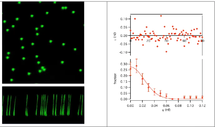
Parallelism of pores has been taken into account in our experiment by irradiated polymers bands scotched on flat holders normal to the beam direction. The parallelism is then directly related to ion track divergence that is mainly due to the placement of a steel window in front of the sample during irradiation. This divergence has been evaluated by confocal laser scanning microscopy (CLSM) imaging of a membrane impregnated by a solution of fluorescent molecules (Alexafluor). This technique provides three dimension images of structures or objects labelled by fluorescent molecules beforehand. Laser causes fluorophores excitation and the consecutive fluorescence of the focal volume (voxel) is measured. Three dimensional scanning of this voxel provides 3D images. Figure 1 shows a typical slice obtained in the xy-plane (top of figure) and the projection of all slices in xz-plane (bottom). Note that the pores radius is smaller than the microscope resolution but fluorescence emission
permits to locate them. Clearly, the pores are not rigorously perpendicular to the membrane surface and are also not parallel to one another. For each slice, the positions of fluorescence spots in the xy-plane have been measured as a function of z, allowing us to compute the distribution of pore angles with respect to their mean orientation (Fig. 1). A Gaussian best fit of this distribution leads to: = 0,023 rd.
This result shows the very small angular deviation of the used set up.
3.2. Bi-conical tracks revealing
To reveal tracks by chemical etching, the track etch-rate vt should be at least 10 times
higher than the bulk etch-rate vb. In order to tune the geometry, the best is to play both on the
polymer chemistry composition to monitor its behaviour towards hydrolysis (vb) and on the
track damages by sensitization techniques such as UV lightening (vt).
If the polymer sensitivity towards hydrolysis is high, then the bulk etch-rate becomes closer to the track etch rate and bi-conical structures are favoured (scheme 1). Polyesters (polycarbonates PC and poly(ethylene terephtalate) PET) are naturally good candidates. Additionally, we have also found interesting alkyl fluorinated copolymers, notably
poly(VHF-co-TrFE), which can undergo double cone track etching by combining the action of a strong
oxidant to create hydrolysable bridges and strong alkaline etchant to cut the bridges inducing polymer chain scissions.
Figure 2 displays FESEM images of a cross-section of track-etched PET and poly(VDF-co-TrFE) membranes. It shows that all constrictions are in the middle of the cross-section with a narrow distribution size. It confirms the uniformity between the tracks and homogeneity of damages all along the ion-tracks.
Under our optimized experimental conditions, we can assume that the track etch-rate vt is
constant. For vb, it is far to be generally true depending the polymer chemical structure.
Indeed, some polymers are very sensitive to ion-irradiation and overcome preferentially chain scissions in the track core or favoured cross-links in the track edges zones. In latter cases, vb is
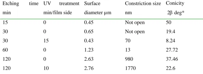
not constant from the track core to the track edges. Poly(VDF-co-TrFE) exhibits a better constant value for vb than PET (Fig. 3). Moreover, the etching times are longer and allow
by using UV sensitization (Table 1). Indeed, UV treatment leads to increase vt and affect also vb.
In Figure 4, there is an example of the finest conicity obtained (28.24°) for bi-conical shaped tracks in a poly(VDF-co-TrFE) copolymer playing on both UV pre-treatment and etching conditions.
4. Magneto-transport behaviour
As a proof of concept that our systems are relevant for studying domain wall in very small constrictions, we use electrodeposition to grow Nickel within the poly (VDF-co-TrFE) membrane previously etched 1h at 80°C corresponding to a constriction size of 13 nm and a conicity of 28° (table 1). A thick Au electrode is first deposited on one side of the membrane and is used as the working electrode. On the other side a very thin gold layer (about 10 nm) is sputtered to signal the stop of the electrodeposition and to contact the biconical wires. This procedure allows contacting only one or a few nanowires for electrical measurements. Details about the method is described elsewhere.11,12 As the constriction is extremely small in an hydrophobic matrix, the electrodeposition time is long. At least 2000s are necessary to fill the 10 µm length of the biconical wire.
Magnetoresistance measurements have been performed as a function of the magnetic field, for a sample composed of a bundle of few tens of Ni nanowires contacted in parallel. The reproducibility from one sample to the other is rather poor, due to the fluctuations of the diameter of the constrictions, and due to the fact that the number of wires contacted in parallel is too small to constitute a statistical ensemble (the thermodynamic limit is not reached). We focus here on a sample that shows the largest constriction effects.
In the case of anisotropic magnetoresistance (AMR), the resistance due to inelastic electron scattering on anisotropic atomic orbitals is higher if the mean trajectory of the electrons is parallel to the magnetization, and lower if it is perpendicular to the magnetization. The electric resistance is then related to the magnetization by a the formula 13
where is the angle between the electric current and the magnetization. In the case of cylindrical wires, 12,13 the current is along the wire axis (so that its density is homogeneous inside the wire) and the magnetization M(H) is uniform. The relation (1) then becomes R(H)=R0 + R (M(H)/Ms)2 where Ms is the magnetization at saturation. The amplitude R of
the AMR is comprised between 1% and 2% in usual Ni nanowires with cylindrical shape (the factor two is due to the contribution of the contact resistance). Accordingly, the hysteresis loop of the resistance gives direct access to the hysteresis loop of the magnetization. In the case of biconical nanowires, the relation (1) is valid only locally (at the scale of a nanometer) since neither the current nor the magnetization is uniform. Numerical simulations are necessary in order to describe precisely the magnetic configurations measured through the magnetoresistance.11 Nevertheless, the profile R(H) gives the mean value of the resistance averaged over a cone section, and the general shape follows approximately that of an uniformly magnetized wire, as shown in Fig. 5 (a). Due to the biconical shape and the contact resistance, the amplitude of the AMR signal is small (typically one order of magnitude below that expected for cylindrical wires). A detailed analysis of similar measurements can be found in reference.12 However, this typical profile is not that measured if a strong constriction is present inside one of the contacted bicones, as shown in Fig. 5(b).
In this case of narrow constriction, the general profile of the curve R(H) is inverted with respect to usual AMR, in the sense that the magnetic configuration perpendicular to the wire axis corresponds to a high resistance. If we assume that Eq. (1) is still valid (i.e. the effect is still due to AMR), the resistance is dominated by a small area (pinned Domain Wall or vortex) in which the inhomogeneous magnetic configuration is not destroyed at ± 1.2 T field.
Figure 6 shows a typical AMR hysteresis loop measured between 1.2 and –1.2 T. The irreversible jumps correspond to the creation (and annihilation) or pinning (and depinning) of a domain wall. The main shape is reproducible with some significant statistical fluctuations of the position of the jumps (six superimposed hysteresis loops are shown in the inset of Fig. 6). In contrast, the plateau corresponding to quasi-static states (pinned and constrained domain walls) are well reproduced. Surprisingly, the most striking feature of this system consists in the systematic relaxation that occurs from unstable states to more stable states. The relaxation mechanisms take different forms, from the typical “instantaneous” thermally activated switch (actually sub-microsecond dynamics) to slow relaxations and slow oscillations.
V. Conclusion
Commercially available PC or PET membranes made by track-etching usually exhibit some non-negligible angular deviations due to the rolling system when irradiating on large scale. The experimental set up at GANIL allows irradiating polymer film on flat supports normal to the beam direction limiting the angular deviation to only 0,023 rd. It is an important parameter to monitor precisely the constriction location of biconical tracks and obtain a good reproducibility between the tracks shape. Two polymer matrices have been studied an hydrophilic and an hydrophobic matrices made of PET and poly(VDF-co-TrFE) respectively. The hydrophobic polymer exhibits a better control of the constriction shape and the access at a larger panel of conicities playing both on the bulk etch rate and the track etch rate. Electrodeposited biconical Ni wires having the smallest constriction size of 13 nm with a conicity of around 20° were chosen for magneto-transport behaviour. Irreversible jumps of the magnetization have been observed, that have been attributed to the pinning and depinning of a constrained magnetic domain wall. A rich variety of relaxation processes have been evidenced showing the singularity of the magnetic configuration involved. Data are still under processing to elucidate the underneath physics. This fabrication process is then promising for studying the propagation and trapping of very small magnetic structures on cylindrical constrictions via the electrical response of the system.
Acknowledgements
The authors want to warmly thank the Direction Générale de l’Armement (DGA, France) (REI08C0035 project) and the Triangle de la physique (RTRA, France) for their financial support. Y. Duchaussoy should find here our deep gratitude for his support at the very beginning of this project three years ago.
References
1. Tatara, G., Zhao, Y.W., Munoz, M., Garcia, N., 1999. Domain wall scattering explains 300 % ballistic magnetoconductance of nanocontacts. Phys. Rev. Lett. 83, 2030-2033
2. Bruno, P., 1999. Theory of interlayer exchange interactions in magnetic multilayers. Phys. Rev. Lett. 83, 2425–2428
3. Gabureac, M., Viret, M., Ott, F., Fermon, C., 2004. Magnetoresistance in nanocontacts induced by magnetostrictive effects. Phys. Rev. B 69,10
4. Viret, M., Berger, S., Gabureac, M., Ott, F., Petej, I., Gregg, J.F., Fermon, C., Francinet, G., Le Goff, G., 2002. Magnetoresistance through a single nickel atom. Phys. Rev. B 66, 22, 220401
5. Montero, M.I., Dumas, R.K., Liu, G., Viret, M., Stoll, O.M., Macedo, W.A.A., Schuller, I.K., 2004. Magnetoresistance of mechanically stable Co nanoconstrictions. Phys. Rev. B 70, 18, 184418
6. Wegrowe, J.E., Wade, T., Hoffer, X., Gravier, L., Bonard, J.M., Ansermet, J.P., 2003. Magnetoresistance of nanocontacts with constrained magnetic domain walls. Phys. Rev. B 67,104418-104424
7. Noh, S.J., Chun, B. S., Wu, H.C., Shvets, I. V., Chu, I. C., Abid, M., Serrano-Guisan, S., Kim, Y. K., 2011. Magnetotransport and Trapping of Magnetic Domain Walls in Spin Valves With Nanoconstrictions. IEEE Trans. Mag. 47, 10, 2436-2439
8. Zambano, A.J., Pratt, W. P., 2004. Detecting domain-wall trapping and motion at a constriction in narrow ferromagnetic wires using perpendicular-current giant magnetoresistance. Appl. Phys. Lett. ,85, 1562-1564
9. Cespedes, O., Bari, M. A., Dennis, C., Versluijs, J. J., Jan, G., O’Sullivan, J., Gregg, J. F., Coey, J. M. D., 2002. Fabrication and characterisation of Ni nanocontacts. J. Magn. Magn. Mater. 242, 492-494
10. Cespedes, O., Watts, S. M., Coey, J. M. D., Dorr, K., Ziese, M., 2005. Magnetoresistance and electrical hysteresis in stable half-metallic La0.7Sr0.3MnO3 and Fe3O4 nanoconstrictions. Appl. Phys. Lett. 87, 083102
11. Biziere, N., Lassalle Ballier, R., Clochard, M.-C., Viret, M., Wade, T. L., Wegrowe, J.E., 2011. Synthesis and magnetic reversal of bi-conical Ni nanostructures. J. Appl. Phys. 110, 063906
12. Wade, T.L., Wegrowe, J.E., 2005. Template synthesis of nanomaterials. European Physical Journal - Applied Physics 29, 1, 3-22
13. Wegrowe, J.-E., Kelly, D., Franck, A., Gilbert, S. E., Ansermet, J. Ph.,1999. Magnetoresistance of ferromagnetic nanowires. Phys. Rev. Lett. 82, 3681-3684
Figure caption
Figure 1: Left: Confocal laser scanning microscopy image of a -PVDF membrane (fluence 5.106cm2, etching-time 3 h) impregnated by a solution of Alexa-488. Top: (xy)-plan. Bottom: projection of (xy)-slices in the (xz)-plan. Right: Top: deviation of pore angle with respect to the normal of (xy)-plane. Bottom: distribution of deviation, mean deviation is= 0:023 rd.
Scheme 1: Track etching considering a constant regime
Figure 2: left: track-etched PET membrane 106 tracks/cm2 78Kr31+ (10MeV/uma) NaOH 2N, 80°C, 7.5 min; right: poly(VDF-co-TrFE) track-etched membrane 106 tracks/cm2 78Kr31+ (10MeV/uma) KOH 10N / KMnO4 0.25N 80°C, 2h.
Figure 3: Bulk etch-rates evolution in PET (left) and poly(VDF-co-TrFE )(right) track-etched membranes
Figure 4: poly(VDF-co-TrFE) track-etched membrane 106 tracks/cm2 78Kr31+ (10MeV/uma) UV pre-treatment 15min and etching in KOH 10N / KMnO4 0.25N solution at 80°C for 30 min. Right: FESEM image of a track section; Left: FESEM image of the replica of a track resulting of half of Ni bi-conical wire after polymer matrix dissolution.
Figure 5: Typical AMR profile measured at angle =90°. (a) Bicones with large constriction. The amplitude of the AMR signal is small due to the contact resistance, and due to the fact that the magnetization is never oriented along the wire axis. (b) Bicones with narrow constriction: AMR profile measured in the same membrane with a different contact.
Figure 6: Resistance as a function of the applied field. The angle of the applied field is 35° with respect to the wire axis. The hysteresis loop is shows the different states of a domain wall jumping from one side of the constriction to the other. Inset: reproducibility over six hysteresis loops.
Figure 1 Scheme 1 t b v v sin If vband vtconstant, t b v v sin If vband vtconstant,
Figure 2 0 0,1 0,2 0,3 0,4 0,5 0 2 4 6 8 10 12 14 16 y = 0,027975 * e^(0,16735x) R2= 0,92912 y = 0,021383x
Etching time (min)
PET R2 = 0.84 0 0,5 1 1,5 2 2,5 3 0 20 40 60 80 100 120 140 y = 0,02975 + 0,021383x R2= 0,99534
Etching time (min) poly(VDF- co-TrFE)
Figure 4
(a) (b)
10,2 10,3 10,4 -1,5 -1 -0.5 0 0.5 1 1,5 R( ) H(T) =35 I = 50 A R/R = 1.7% 10,2 10,4 -1 0 1 Figure 6
Table caption
Table 1: Constrictions sizes and conicities for various etching conditions for SHI irradiated poly(VDF-co-TrFE) polymer films. Etching temperature was set at 80°C and etching solution was composed of KOH 10N / KMnO4 0.25N.
Etching time min UV treatment min/film side Surface diameter µm Constriction size nm Conicity 2 deg* 15 0 0.45 Not open 50 30 0 0.65 Not open 19.4 30 15 0.43 70 8.24 60 0 1.23 13 27.72 120 0 2.63 980 37.46 120 10 2.76 1770 22.6
* = 2.arctan((x1-x2)/2d) where x1and x2 are two diameters measured on FESEM images of track sections and d
is the distance between x1and x2.