HAL Id: hal-01181180
https://hal.archives-ouvertes.fr/hal-01181180
Submitted on 29 Jul 2015
HAL is a multi-disciplinary open access
archive for the deposit and dissemination of
sci-entific research documents, whether they are
pub-lished or not. The documents may come from
teaching and research institutions in France or
abroad, or from public or private research centers.
L’archive ouverte pluridisciplinaire HAL, est
destinée au dépôt et à la diffusion de documents
scientifiques de niveau recherche, publiés ou non,
émanant des établissements d’enseignement et de
recherche français ou étrangers, des laboratoires
publics ou privés.
H
∞ loop shaping control for distributed PLL network
Anton Korniienko, E Colinet, Gérard Scorletti, Eric Blanco
To cite this version:
Anton Korniienko, E Colinet, Gérard Scorletti, Eric Blanco.
H
∞ loop shaping control for
dis-tributed PLL network.
2009 IEEE PRIME, IEEE, Jul 2009, Cork, Ireland.
pp.336 - 339,
H
∞
loop shaping control for distributed PLL network
A. Korniienko, E. Colinet,
CEA, LETI, MINATEC 17 rue des martyrs, 38054 Grenoble Cedex 9, France
anton.korniienko@cea.fr,
G. Scorletti, E. Blanco
AMPERE, ECL 36 avenue Guy de Collongue,
69134 Ecully Cedex France
Abstract — In this paper, we describe a robust control law for distributed PLL network using H∞ optimization problem. The
controller can be uniformly applied on all distributed nodes and guarantees good stability margins, enhanced performance and reduced jitter noise. A 2-dimensional Cartesian mesh network structure is considered without using any feedback loop phase information propagation to eliminate undesirable mode-locked states.
I. INTRODUCTION
Balanced trees are introduced in most modern synchronous digital integrated circuits and microprocessor systems in order to distribute the clock [1]. The clock tree synchronization is achieved by appropriate propagation delays which may be complex to implement. In large circuits, it becomes very difficult and even impossible to deploy the tree exactly as desired which decreases the clock accuracy significantly. Moreover, for gigahertz clock speed, the skew and the jitter are induced by the random variations in gate and interconnection delays [2]. Even in a well-designed and well-balanced clock distribution network, the distributed clock buffers and inter-line coupling between clock wires are major sources of skew and jitter. Therefore, as clock speed increases, signal delay across a chip becomes comparable to a clock cycle which implies computation errors. Moreover, the clock distribution network of a modern microprocessor consumes a significant fraction of the total chip power because of important parasitic impedances due to many close wires. Then, it has a major impact on the overall performance of the system.
An interesting alternative to the conventional balanced tree is the active clock distribution networks whose nodes consist on Phase Locked Loops (PLLs). The idea is to compare the delay between neighbor nodes and adjust if it is necessary. This structure has a local clock generation regularly distributed which reduces the jitter accumulation. Since wires are only used to interconnect neighbor nodes, there are no important parasitic impedances reducing the power consumption.
Secondly, the proposed structure only requires local synchronization between neighbor nodes to generate globally synchronous clock without skew. The absence of strong matching requirement and the regularity reduce the chip complexity and its cost.
In order to deploy this approach, it is necessary to design the filter of each PLL and to choose the general network structure. This choice is crucial because of the mode-locking problem where constant non zero differences can exist between PLL oscillator phases.
In this paper, we propose an original solution to these issues. The PLL filter is designed using H∞ loop-shaping method [3].
Furthermore, we propose a network structure in order to avoid the mode-locking problem where feedback loops are not introduced.
The design of the PLL filter is presented in Section II. The problem of mode-locking with respect to different network structures is discussed in Section III. These different points are illustrated by simulations in Section IV.
II. PLLDESCRIPTION
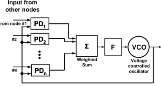
Each node of the clock distribution network is realized by a multi input phase-locked loop (PLL). This PLL, see Fig. 1, is made of a voltage controlled oscillator (VCO) with a filter F. The feedback loop is designed in order to synchronize in phase the local oscillator with the combination of multiple reference signals. The oscillator phase is compared to the reference signals with the Phase Detectors (PDs) using analog multiplication. The outputs of these PDs are summed together and the result (the average signal) is filtered by F. When locked, the local oscillator signal and the average signal are expected to have identical frequency and phase in the steady state [4].
PD1 PD1 PD2 PD2 PDn PDn Σ Σ F VCO Input from other nodes from node #1 #2 #n Weighted
Sum controlled Voltage oscillator
Fig. 1 Multiple input phase-locked loop
From a control system point of view, a node is represented by the linear block diagram of Fig. 2 in the phase domain.
from node #1 F(s) 1/s Phases from other nodes #2 #n Sum Voltage controlled oscillator Σ Σ 1/n1/n + -Local phase ωreft+φref ωit+φi
Fig. 2 Linear multiple input PLL model
In Fig.2, the reference signal is the average of the neighbor node phases. F(s) represents the filter transfer function to be designed. The VCO is modeled by a simple integrator referred as G(s). Since the reference signal is a ramp, the open loop transfer function G(s).F(s) must have two integrators in order to achieve a zero stationary error (tracking performance, type-II PLL). Thus, an integrator has to be introduced in the filter F(s). In addition, F(s) has to be low-pass in order to reject the jitter (noise reduction) and the high frequency components induced by the phase detectors. The response time of the feedback loop is specified by the bandwidth of the open loop transfer function G(s).F(s). Since the open loop transfer function G(s).F(s) contains two integrators, the stability of the closed loop system is difficult to ensure which motivates the use of a rigorous design method for the filter. Furthermore, since the same filter is designed and applied for different VCOs, robust stability to parameters uncertainty (due to technological dispersions) has to be guaranteed. For these reasons, we propose to use a H∞ filter
design approach. It gives the optimal filter that guarantees the performance requirements as well as the best achievable stability margins.
A. Filter design using the H∞ loop-shaping approach
The loop-shaping method consists in specifying a filter Wc to obtain a desired open-loop shape presenting the different specifications defined before. Once Wc is designed, the H∞ optimization problem is applied on the extended system G(s).Wc(s) giving the minimum upper bound for the so-called H∞ norm of the stable achievable closed loop system and finds the controller
K. This ensures an a priori guarantee of robust stability and tracking performance of the feedback loop. The final filter F is then obtained by the product Wc.K.
The loop shaping specifications are described by the following: An integrator is enforced in F(s) by introducing an integrator in Wc. Good reference tracking can be achieved when the gain of G(s).F(s) is high in low frequencies. To do so, Wc(s) is designed with a high gain in this frequency range. Noise reduction can be achieved when the gain of G(s).F(s) is low in high frequencies. This is obtained by setting Wc(s) with a low gain at high frequency. The desired bandwidth of the open loop transfer function G(s).F(s) is approximately given by the bandwidth of G(s).Wc(s).
In the optimization problem, G.Wc is represented by the minimal state space representation: GWc:
t x C t y t u B t x A t x . . . (1) K is then obtained in the form of the state space representation [5]:K:
. . . K K K K K K x t A x t B y t u t C x t (2)with T 2 T K A A BB X Z YC C 2 T K B Z YC T K C B X
2
1 n n Z I YX I X and Y are the positive definite matrices which are solutions of the two following Riccati equations: 0 0 T T T T T T XA A X XBB X C C YA AY YC CY BB (3)
and where is a real positive scalar slightly higher then min 1sup
X Y.
. The order of the filter obtained by this method is usually equal to the sum of the order of G with twice the order of Wc. Using reduction model methods [6], a filter with a lower order but with a similar level of performance can be obtained which is essential for the practical implementation of the filter.III. NETWORK STRUCTURE
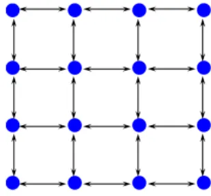
The principle of synchronization described in Section II can be applied for networks having many nodes with multiple connections. In this paper, we consider the synchronization of a 2-dimensional Cartesian mesh networks like the one in Fig.3. This network has a regular topology.
Fig. 3 Considered network topology
Supposing that every node of the network is synchronized in phase with its neighbor node (in average) as shown in Fig.3 and Fig.1, we shall expect that the overall network is globally synchronized in steady state. Unfortunately, because of the cyclic nature and modularity of the phase, this is not always true. This undesired case, known as mode-locking [6-7], can be observed in the example of a 2x2 network presented in Fig.4. As the phase is cyclic, in this particular configuration, the effect of a neighbor phase cancels exactly the effect of the other one for every node. The total influence on every node is zero and despite the fact that their global phases are unequal, there is no reason for the node phases to change and the network stays in this stable stationary point.
φ
1= 0
φ
4= π/2
φ
2= -π/2
φ
3= π
Fig. 4 Mode-locking in a 2x2 network
Mode-locking can be avoided by ensuring that no feedback loop exists in the propagation of the phase information [2,7] (Fig.5). Another possible alternative is presented in [7-8] where the authors prove that the PLL synchronization issue can also be solved using special phase detectors which must have a response with negative slope beyond a phase difference of 90˚.
Fig. 5 Phase information propagation
In the case of no feedback loop, the stability of all the nodes implies the stability of the overall network. This property is not a priori ensured in the case of feedback loop network except when it is explicitly demonstrated as in [7-8].
IV. SIMULATION RESULTS
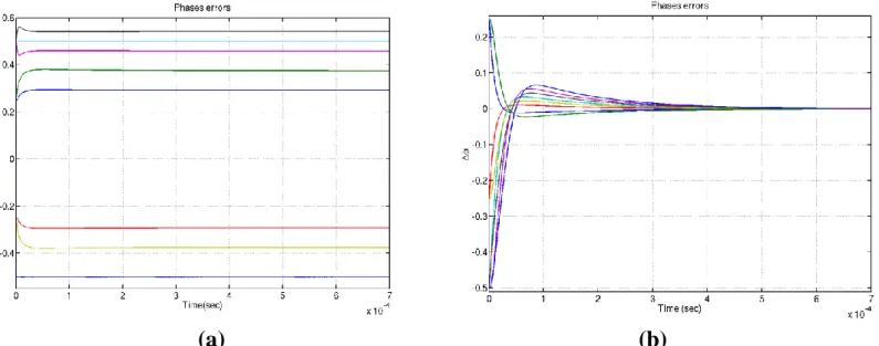
To illustrate the previous section, the simulation of coupled 3x3 PLL network has been realized for two case studies: with and without feedback loop phase information propagation, see Fig.6 (a,b respectively). In both cases, the first node was chosen as a reference signal with a frequency of 20 MHz and the other nodes operated with the same free running frequency and a randomly initialized phase. In this simulation, in order to illustrate the mode-locking avoidance, the PLL was realized with non linear phase detectors as presented in Fig.1. The VCO of each node are modeled as pure integrator in the phase domain.
We first focus on the design of the filter F. To this purpose, we choose the Wc filter as follows:
6
10 10 26 . 1 6283 10 96 . 78 s s s WC (4)in order to obtain an open-loop bandwidth close to c 4 105rad/ secand a filter F presenting an integrator and a low pass filter characteristics. The solution of the Riccati equation was computed using Matlab with the Control System Toolbox:
min 1.65
was obtained.
Ref Ref
(a)
(b)
Fig. 6 Simulation network with (a) and without (b) feedback loop phase information propagation The filter was then reduced to the following transfer function:
2 6 12
17 10 77 . 6 10 63 . 4 6175 10 91 . 28 s s s s F (5)Note that the result of H∞ optimization gives a robust filter that is stable and efficient not only for one system but for a set
of systems with dispersed parameters. Thus, the same filter can be used for each nodes of the network.
In Fig.7, the magnitude and the phase of desired and obtained open-loop transfer function are presented. There is no significant difference between both transfer functions.
Fig. 7 Bode diagrams of the G.Wc (blue dashed line) and the final open-loop transfer function G.F computed via H∞ loop
shaping (red full line)
To avoid the mode-locking in this simulation the network without feedback loop phase information propagation was considered. The efficiency of this approach is illustrated in Fig.8 showing the simulation results for the case with and without feedback loop phase information propagation (Fig. 8 a) and b) respectively). As it can be seen, in the second case, the coupled PLL network is synchronized even if the initial phase values are close to the mode-locking values.
CONCLUSION
The clock distributed structure with locally generated independent clocks was described in this paper and a robust filter was designed. In the case of no feedback loop network, the filter guarantees stability of the overall network. Furthermore, this network structure ensures the synchronization of the local oscillators by avoiding the mode-locking due to the cyclic nature of the phase. The simulation results illustrate the realness of the proposed approach. The standard H∞ filter design approach using the weighting functions
presents an interesting and a perspective evolution of this work. Comparing to H∞ Loop shaping design, it should reduce the network
consumption by limiting the control signal power while ensuring the optimal stability and the error tracking performances. ACKNOWLEDGEMENTS
This work was supported by the French National Agency of Research (ANR) through HODISS project.
(a)
(b)
REFERENCES
[1] E. G. Friedman, “Clock Distribution Networks in Synchronous Digital Integrated Circuits”, Proceedings of the IEEE, May 2001, Vol. 89, No. 5, pp. 665-692. [2] M. Saint-Laurent and M. Swaminathan, “A multi-PLL clock distribution architecture for gigascale integration”, IEEE Computer Society Workshop VLSI, May
2001, pp. 30-35.
[3] C. Kharrat, E. Colinet, A. Voda, “H∞ Loop shaping control for PLL-based mechanical resonance tracking in NEMS resonant mass sensors”, Sensors, IEEE,
October 2008, pp.1135-1138.
[4] T. Saito, “Application of Phase-Locked Oscillator for PCM Network Synchronization”, IEEE Transaction on communications, October 1982, Vol. 30, No. 10, pp. 2344–2354.
[5] G. Duc, S. Font, “Commande H-infini et mu-analyse, des outils pour la robustesse”, Ed. Hermès, 1999.
[6] G. Scorletti et V. Fromion. “Introduction à la commande multivariable des systèmes : méthodes de synthèse fréquentielle H∞”. Cours de 3A Instrumentation
Automatique de l’ENSI de Caen et du Master Recherche 2A ESCI de l’Université de Caen, 2005, 213 pages.
[7] G. A. Pratt, and J. Nguyen, “Distributed Synchronous Clocking”, IEEE Transactions on Parallel and Distributed System, March 1995, Vol. 6, No. 3, pp. 314-328. [8] V. Gutnik, and A. P. Chandrakasan, “Active GHz Clock Network Using Distributed PLLs”, IEEE Journal of Solid-State Circuits, November 2000, Vol. 35, No.