HAL Id: hal-03050853
https://hal.archives-ouvertes.fr/hal-03050853
Submitted on 10 Dec 2020
HAL is a multi-disciplinary open access
archive for the deposit and dissemination of
sci-entific research documents, whether they are
pub-lished or not. The documents may come from
teaching and research institutions in France or
abroad, or from public or private research centers.
L’archive ouverte pluridisciplinaire HAL, est
destinée au dépôt et à la diffusion de documents
scientifiques de niveau recherche, publiés ou non,
émanant des établissements d’enseignement et de
recherche français ou étrangers, des laboratoires
publics ou privés.
Growth evolution of N-polar indium-rich InAlN layer on
c-sapphire via strain relaxation by ultrathin AlON
interlayer
Prerna Chauhan, S. Hasenöhrl, A. Minj, M.P. Chauvat, Pierre Ruterana, J.
Kuzmík
To cite this version:
Prerna Chauhan, S. Hasenöhrl, A. Minj, M.P. Chauvat, Pierre Ruterana, et al.. Growth evolution of
N-polar indium-rich InAlN layer on c-sapphire via strain relaxation by ultrathin AlON interlayer. Applied
Surface Science, Elsevier, 2020, 502, pp.144086. �10.1016/j.apsusc.2019.144086�. �hal-03050853�
UNCORRECTED
PROOF
Contents lists available at ScienceDirect
Applied Surface Science
journal homepage: http://ees.elsevier.com
Growth evolution of N-polar indium-rich InAlN layer on c-sapphire via strain
relaxation by ultrathin AlON interlayer
Prerna Chauhan
a, S. Hasenöhrl
a, A. Minj
c, M.P. Chauvat
b, P. Ruterana
b, J. Kuzmík
aaInstitute of Electrical Engineering, Slovak Academy of Sciences, Bratislava, Slovakia bCIMAP, UMR 6252 CNRS, 6 Boulevard Maréchal Juin, 14050 Caen, France cIMEC, Kapeldreef 75, Heverlee 3001, Belgium
A R T I C L E I N F O
KeywordsIndium-rich InAlN layer Growth evolution
Kelvin probe force microscopy High-resolution transmission electron mi-croscopy
Energy dispersive X-ray spectroscopy High-angle annular dark-field
A B S T R A C T
InAlN as a functional inorganic material is a promising alternative to the commonly used InGaN in tunnel diodes and optoelectronic devices, due to its tunable wider range of energy bandgap (0.65–6.2eV), thus empowering utilization of the whole solar spectrum. Moreover, high electron drift velocity and carrier concentration are con-sidered as the most desirable prerequisite of indium-rich InAlN. N-polar indium-rich InAlN could be more ben-eficial due to the reverse direction of the polarization compared to Ga-polar. However, unanswered questions persist concerning growth evolution of N-polar indium-rich InAlN grown by organometallic chemical vapor de-position (OMCVD). In this study, energy dispersive X-ray spectroscopy (EDX) and high-angle annular dark-field (HAADF) imaging are used to characterize N-polar layer at nanometer scale in order to determine the evolution of the layer on (0001) sapphire substrate. Long nitridation of sapphire substrate leading to the for-mation of ~2nm AlON ultrathin interlayer, which relaxes strain at the InAlN/sapphire interface with assistance of a low-temperature AlN interlayer is observed. EDX analysis confirms that after strain relaxation of InAlN layer, the indium-incorporation has only a weak dependence on the polarity of the layer. The incorporation of indium at preferential sites is also discussed at length.
1. Introduction
N-polar (In,Ga)N-based heterostructures are attracting a remarkable amount of attention in the past years. The most promising application potential is expected for the high electron mobility transistors (HEMTs) [1], tunnel junction diodes [2] and optoelectronic devices, like solar cells [3] and light-emitting diodes (LEDs) [4]. On the contrary, inves-tigation of its counterpart InAlN mainly revolved around achieving the lattice matched (LM) conditions to GaN buffer layer for the applica-tion in HEMTs. In such applicaapplica-tions, it is used as a thin barrier layer for Ga-polar materials [5], and as a strong back-barrier for N-polar [6]. Other previously reported devices involving similar heterostruc-tures were distributed Bragg reflectors [7], and intersubband photode-tectors [8]. Recently [9,10], we demonstrated the epitaxial growth of metal-polar and N-polar InAlN buffer layers by organometallic chemical vapor deposition (OMCVD) that opened the possibility of growing InN channel transistor heterostructures on indium-rich InAlN buffer layer for THz applications, and optoelectronic devices as well [3,4]. Although significant advances have been made on devices utilizing LM InAlN/GaN heterostructure on metal-polar and N-polar materials, only a little atten-tion has been given to N-polar indium-rich InAlN.
The vast majority of studies have explored strarelaxation and in-dium-incorporation mechanisms on metal-polar [11] and N-polar [12] InGaN/GaN
systems, covering the indium content range from low to moderate. These studies relate the strain relaxation mechanism and/or the associated ef-fect of indium-incorporation to the formation of the misfit dislocations via slip system (mainly present in the low-indium content regime), al-loy ordering, formation of V-defects, indium-rich interfacial regions and stacking faults.
On the other hand, understanding the growth of InAlN requires fo-cused attention as it faces a separate set of challenges when compared to its counterpart InGaN. For example, it remains unclear why the most fundamental relaxation mechanism proceeding via slip system is not of-ten triggered in strained InAlN [13]. Even, the intrinsic degradation uti-lizing the spontaneous formation of V-pits not associated with underly-ing threadunderly-ing dislocations is reported to occur in coherently grown mis-matched and LM InAlN on GaN [14]. Furthermore, theoretical investi-gations also predict strong alloy immiscibility, i.e., a phase separation over a broad range of indium content of InAlN [15]. These issues indi-cate that stringent OMCVD growth conditions are required for the fab-rication of high-quality indium-rich InAlN layer. Consequently, for its more profound understanding, a study of the growth evolution of in-dium-rich InAlN layer is necessary.
Recently, we reported the growth of a thick N-polar N layer directly on c-plane sapphire exhibiting a highly efficient red lu-minescence [10]. However, the evolutionary process of Indium-incor-poration along the growth direction [0001] of N-polar indium-rich InAlN layer and the local growth dy
E-mail address: prerna.chauhan@savba.sk (P. Chauhan) https://doi.org/10.1016/j.apsusc.2019.144086
Received 12 August 2019; Received in revised form 12 September 2019; Accepted 17 September 2019 Available online xxx
UNCORRECTED
PROOF
P. Chauhan et al. Applied Surface Science xxx (xxxx) xxx-xxx
namics by which indium is preferentially incorporated during the sub-sequent InAlN layer growth on sapphire are presently unidentified. Our current work provides a significant insight into the growth evolution of N-polar indium-rich InAlN layer on sapphire. We systematically inves-tigated the surface features by Kelvin probe force microscopy (KPFM). Subsequently, to achieve in-depth understanding, the cross-sectional analysis by high-resolution transmission electron microscopy (HRTEM) and scanning transmission electron microscopy (STEM) were employed to elucidate the effect of polarity vs. strain in indium-incorporation in the InAlN layer.
2. Experiments
Epi-ready c-plane or (0001) sapphire ( ) substrate was nitri-dated under the ammonia ( ) flow of 3000 sccm at 1011°C for 300s and followed by the growth of AlN and InAlN layer at 730°C for 30s and 8440s, respectively. The preprocessing and growth were performed by AIXTRON 3X2″ flip-top (FT) close coupled showerhead (CCS) reactor OMCVD system. Precursors used for In, Al, and N were trimethylindium (TMIn), trimethylaluminum (TMAl) and , respectively. Other details of the growth can be found elsewhere [10]. The resultant N-polar re-laxed 334nm thick layer was investigated in this study.
Surface structural and electrical properties were studied using atomic force microscopy (AFM). The tapping surface imaging mode was uti-lized for quantitative statistical analysis of characteristics related to surface topography, compositional inhomogeneity, surface-exposed de-fects such as dislocations and/or V-pits and for any other anomalies. The nanoscale surface potential mapping was implemented by employ-ing KPFM in the amplitude-modulation mode. In this mode, the sur-face topography simultaneously with the KPFM map was acquired. The KPFM measurements were done under a constant-amplitude mode
at the first harmonic of the AFM probe cantilever (~55kHz) using a tip AC bias of 3V serving as the modulating electrostatic signal at ~346kHz, the second harmonic of the cantilever. For the measure-ments, the sample was grounded, the tip-sample separation was close to 10nm, the scan speed was set to 0.5 lines/second and Pt/Ir-coated Si-AFM probes with the tip radius of 25nm were used. All the AFM based measurements were performed on CSI Nano-Observer AFM under ambient conditions.
The samples for TEM observations were prepared using a focused ion beam (FIB) machine. The weak beam analysis was carried out to an-alyze the crystallographic quality of the layer using a JEOL 2010 mi-croscope. The energy dispersive X-ray spectroscopy (EDX) and high-an-gle annular dark-field (HAADF) investigations took place in a double Cs corrected JEOL 200F STEM. This allowed a spatially-resolved chem-ical analysis using EDX. In HAADF, the contrast is mainly given by the atomic number (Z-contrast) and is employed to distinguish between In (high Z=bright contrast) and Al (low Z=dark contrast).
3. Results
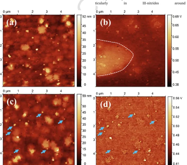
In Fig. 1(b), the surface potential map also referred to as con-tact potential difference (CPD) map obtained via KPFM shows alloy inhomogeneity in InAlN at the micrometer scale. In this Figure, the region with a brighter contrast, demarcated by a white dashed-line, corresponds to an area with enhanced CPD or equivalently to a drop in the work function by 0.2eV. Considering the work function trend in the following order GaN>AlN>InN as published by Strak et al. [16], the reduced work function implies a higher indium-molar frac-tion in InAlN. However, the work funcfrac-tion change can be dominated by the local fluctuation of surface and sub-surface fixed charges rather than by the alloy fluctuation. This behavior has been observed par-ticularly in III-nitrides around the
Fig. 1. (a) and (c) Topography and (b) and (d) their corresponding KPFM images of the N-polar InAlN layer over the scan area of 5x5 . 2
UNCORRECTED
PROOF
extended defects such as dislocations and V-pits [17,18]. In our case, the pits (~2.6–6.6× ) or dislocations present at the periphery of grains (in Fig. 1(a)) appear with a contrast in KPFM map correspond-ing to a higher work function but strictly within the confinement of the pit. This, however, cannot be related to possible fixed charges or trapped electrons at the dislocations since a charged dislocation would result in the dispersive nature of the potential or CPD change around it of the type ~ - with r being the radial distance from the disloca-tion core and R the radius of the space charge region containing dislo-cation core [19].This type of behavior is usually observed in InAl(Ga)N and even in InGaN where the V-shaped pits with high electron affinity over their semi-polar surfaces contribute to the locally enhanced work function [20].
In addition to grains and pits, localized growth features with an av-erage diameter of 153±26.3nm and a peak height of 22±7.9nm (in-dicated by arrows in Fig. 1(c) and (d)) surrounded by partially-visible trenches or pits were also observed. These growth anomalies with a sur-face density of ~1× estimated over 5×5 are associated with a much lower work function changes of only 30meV with respect to the background (Fig. 1(d)). This drop in the work function could cor-respond to a local increase in indium content facilitated by increased growth rate or could also indicate the change in or even a reversal of surface polarity. The ab-initio calculations by Strak et al. [16] predict a lower magnitude of work function in metal-polar III-nitride surfaces in comparison to N-polar surfaces. Since the work function drop mea-sured by KPFM is considerably smaller, several other factors contribut-ing to the work function includcontribut-ing charged defects cannot be fully ex-cluded. Therefore, in order to have a more in-depth insight, these anom-alies were further investigated by HRTEM and EDX analysis, which will be discussed in the next section.
Figs. 2 and 3 display the microstructure of the investigated In-AlN/sapphire heterostructure. Fig. 2(a) shows a weak beam dark-field image recorded using g=0002, and Fig. 2(b) shows the correspond-ing bright-field image. The surface morphology is not planar due to the brighter feature in Fig. 2(a), which extends from the interface up to the surface. This feature originates most probably from a lighter ma-terial at the heterointerface level as demonstrated by the correspond-ing whiter contrast in Fig. 2(b). All along the interface, higher con
trast is present, which decreases gradually within the first 40nm of layer growth. Moreover, few screw-type threading dislocations (TD) are also visible in the InAlN layer. In Fig. 3, using g=10–10, it is challenging to attain the weak beam conditions and the predominant contrast indi-cates mainly the presence of strain in the basal planes all along the layer without any possibility to distinguish individual defects, such as disloca-tions, stacking faults, or inversion domain boundaries [21,22].
This illustration gets more evident in the HAADF image (Fig. 4), where a similar feature is analyzed along a different projection direc-tion and exhibits higher growth rate than the adjacent areas. The rapidly growing small features with the surface density ~1× as dis-cussed in previous KPFM section are the metal-polarity patches [23], which originate from Al-rich areas just at the interface (as shown in Figs. 2–4) in the N-polar layer [10]. Moreover, all over the heteroin-terface, irregular distribution of the darker contrast is clearly visible with an extension of around 40nm. This indicates that an irregular Al-rich interfacial layer (dark contrast) due to the irregular chemical dis-tribution may lead to the strain relaxation followed by an increase of the indium-incorporation in the subsequent homogeneous InAlN layer. This assertion is further supported by the bright contrast of homoge-neous area which depicts more indium content. This is consistent with the transition and homogeneous regions observed in AES depth profile shown in Ref. [10]. The origin of the columnar formation is due to the faster growth of In/Al inversion domains (IDs) in N-polar matrix [24]. However, a possible contribution of screw dislocations generated at the interface during nitridation [25] cannot be completely excluded as these areas are highly disordered.
To analyze the growth evolution, a detailed investigation of the el-emental distribution along the direction of growth and local preferen-tial incorporation centers is essenpreferen-tial. Fig. 5 shows a STEM-HAADF mi-crograph of InAlN layer. The indium-molar fractions of the layer were measured at six different places. Out of six EDX line scans, the first scan is parallel to the InAlN/sapphire interface and the remaining scans are along the direction of growth. To be more specific, the second and fourth EDX line scans are along the periphery of the columnar struc-ture and the third is at its center. The EDX line scans in Fig. 5 show the probe position during EDX acquisition, where five points were ana
Fig. 2. Microstructural features as pointed out by conventional TEM in N-polar InAlN layer: (a) Weak beam image recorded using g=0002, a bright feature that stems from the interface
to the surface. (b) The corresponding bright field shows surface pinholes as well as light contrast at the bottom of the bright feature of (a).
Fig. 3. Microstructural features as pointed out by conventional TEM in N-polar InAlN layer: (a) Weak beam image with g=10–10. (b) The corresponding bright field image.
UNCORRECTED
PROOF
P. Chauhan et al. Applied Surface Science xxx (xxxx) xxx-xxx
Fig. 4. HAADF image recorded along < > zone axis of N-polar InAlN layer on sap-phire: the red arrow points to a columnar structure originated at an Al rich area (black feature). (For interpretation of the references to colour in this figure legend, the reader is referred to the web version of this article.)
Fig. 5. Cross-sectional HAADF-STEM image of N-polar InAlN layer along < > zone axis, six solid lines each with five analyzed data points show the position of EDX line scans across the InAlN layer. Color bar along with each line scan shows the correspond-ing Indium-molar fraction as a function of position. (For interpretation of the references to colour in this figure legend, the reader is referred to the web version of this article.)
lyzed and the corresponding molar fraction is shown. While being metal-polar predominantly observed the indium-molar fraction in columnar structure varies from 0.60 to 0.66 except for one point at pe-riphery where the indium-molar fraction of 0.74 is observed. This could be ascribed to an enhanced incorporation of indium and formation of InN chains in the vicinity of dislocation core.
On the other hand, the indium-molar fraction in the N-polar re-gion varies from 0.60 to 0.71. Close to interface the indium-molar fraction is close to 0.64±0.04 as derived from XRD, which averages over the whole layer and all compositional fluctuations influence the FWHM. STEM-EDX analysis indicates that the range of the indium-mo-lar fraction varies from 0.60 at interface to 0.74 close to surface. This EDX data confirm the local compositional inhomo
geneities that lead to the broad width (FWHM=0.20°) of 0002 dif-fraction peak of InAlN layer as shown in Ref. [10]. As demonstrated in Figure 5, the observed indium-molar fraction varied from 0.60 to 0.74 in InAlN layer. These inhomogeneities are presumably composed of nanoscopic indium-rich phases, unlike the macroscopic phases that are volumetrically large enough to be detected in 2θ/ω scan of XRD.
For a more comprehensive analysis of the growth evolution, we widened up the investigations and focused on the InAlN/sapphire inter-face. Fig. 6(a) shows the HAADF image of the heterointerinter-face. At the top of sapphire, a dark interfacial area of ~2nm thickness is marked by the white arrows. The displayed contrast validates that the mean atomic number is smaller than that of InAlN and sapphire. This is further con-firmed by the EDX analysis of the area as indicated by the green rec-tangle in Fig. 6(a). The corresponding spectrum displayed in Fig. 6(b) shows the oxygen (O) peak along with the expected nitrogen (N) and aluminum (Al) peaks. Thus, our analysis reveals the existence of crys-talline AlON interlayer formed during 300s long nitridation, which is described as the N-rich growth. Sapphire ( ) substrate is the source of Al and O [10]. The subsequent growth of low-temperature (LT) AlN interlayer weakens the diffusion of O atoms into AlN interlayer and the following InAlN layer.
In the HAADF image shown in Fig. 7(a), this intermediate layer is highlighted by two arrows where the white arrow underlines the sap-phire surface, and the red arrow points to the bottom of the InAlN layer. In the corresponding filtered image (Fig. 7(b)), the interface disloca-tions are clearly visible and the misfit dislocadisloca-tions discernible at the ter-mination of each atomic plane. At the AlON/sapphire interface, nine misfit dislocations are present and separated by an average distance of 2nm as marked by the white asterisks in the observed image, whereas only three misfit dislocations (marked by the black asterisks) are pre-sent at the InAlN/AlON interface or at the bottom of the InAlN layer. This image shows the 8:10 relationship between AlON and sapphire, meaning that roughly eight Al–Al atomic distances in AlON correspond to ten Al–Al atomic distances in sapphire. Another existing relationship is 14:16. This is a clear indication that most of the plastic strain corre-sponding to the large lattice mismatch (~22%) between sapphire and layer is released at interface via the formation of misfit dis-locations which is consistent with the first-principles calculations [26] and our previous XRD analysis [10].
4. Discussion
Before starting the discussion, we would like to briefly summarize our main experimental results. HAADF and EDX data show the presence of an intermediate layer ~2nm, which is a mixture of Al-O-N. It can be seen that the interfacial layer is crystalline and has the same crystal structure as the top InAlN, and it carries out the strain relaxation with the two series of misfit dislocations. Most of the interface strain is re-leased at the interface of AlON/sapphire with the formation of misfit dislocations.
The InAlN/sapphire interface is highly complex and can be en-visioned as follows. In the initial stage of nitridation of sapphire ( ) at 1011°C a
two-Fig. 6. (a) Cross-sectional HAADF image of the InAlN/sapphire interface recorded along < > zone axis of InAlN. A two-dimensional continuous and crystalline interlayer in darker contrast is visible on top of the sapphire. A green rectangle marked in the interlayer shows the location of EDX measurement area and (b) the corresponding EDX spectrum showing the only contributions of Al, O and N in the area. (For interpretation of the references to colour in this figure legend, the reader is referred to the web version of this article.)
UNCORRECTED
PROOF
Fig. 7. (a) Cross-sectional HAADF image of the AlON interlayer between sapphire and InAlN layer recorded along < > zone axis of InAlN. The white arrow points to the AlON/ sapphire interface while the red arrow points to the InAlN/AlON interface. (b) The corresponding filtered lattice image of (a) highlights the misfit dislocation network. The white asterisks mark the misfit dislocations at the sapphire/AlON interface and the black asterisks locate the few misfit dislocations at the InAlN/AlON interface.
dimensional layer of aluminum-oxynitride ( ) forms [27]. That results in the N-polar AlN due to the dissociation of AlON. With the in-creasing duration of nitridation, the layer transforms into three-dimen-sional layer through the formation of Al-polar AlN islands. The layer grown after the nitridation is mainly N-polar but exhibits columnar structures via the formation of inversion domains at the sites of Al-polar AlN islands in AlON layer, as illustrated in Fig. 8(a). The islands as the inversion domains are the fast-growing metal-polar area inside the N-po-lar matrix and form highly disordered columnar structure (Fig. 8(b)). Moreover, the growth of InAlN layer under N-rich growth condition pre-serves the N-polarity established by AlON interlayer.
At a low growth pressure, the enhanced surface mobility of indium-and Al-adatoms indium-and their stronger bonding with nitrogen surface atoms of the N-polar layer contribute to the enhanced indium-incorporation [28]. This indicates that after partial strain relaxation at the InAlN/sap-phire interface via the AlON layer, in 40nm wide transition region an-other factor that influences the indium-molar fraction of the layers is the polarity of InAlN layer. The strain relaxation and N-polarity accom-plished the compositional grading in transition region, and finally a re-laxed InAlN layer was formed but with local compositional fluctuation in the indium-molar fraction. Although, the weak interaction between the impinging indium- and Al-adatoms with the indium- and Al-sur-face atoms of metal-polar layer leads to the lesser indium-incorporation [28]. In this case under the used growth temperature of 730°C, the in-dium-desorption has presumably influence on the layer growth.
The surface topography (Fig. 1) of InAlN layer confirms the Volmer-Weber growth mode that describes the nucleation and subse-quent growth of distinct islands at the preferential sites provided by nitridation and/or AlN thin layer on sapphire. As suggested by Nix [29] and Sheldon et al. [30], coalesced crystallites impose displace-ments or tensile elastic strain at the grain boundary. Usually, the mode of relaxation is controlled by temperature, compositional grading or surfactants [31]. Thus, it is proposed that the strain relaxation mech
Fig. 8. Schematic illustration of In/Al-polar inversion domain formation mechanism in the
N-polar InAlN layer. The colors and arrows indicate the polarity of the layer: blue color and upwards arrow- In/Al-polar; red color and downwards arrow- N-polar. (a) Sapphire ( ) annealing in for 300s results in evolution of stable Al-polar AlN islands along with layer. (b) During the further growth of InAlN layer, the islands promote metal-polar columnar structure, while the layer decomposes to give N-polar In-AlN. (For interpretation of the references to colour in this figure legend, the reader is re-ferred to the web version of this article.)
anism is changed in the InAlN layer grown on sapphire because of the different surface kinetics of indium as a surfactant. The indium-surfac-tant effect on nitrides during OMCVD growth was investigated earlier theoretically [32] and experimentally [33]. When indium as a surfac-tant is involved in growth, an increase of the surface diffusion length that enhances the step-flow growth mode is expected. In the presence of fast-growing metal-polar inversion domains and/or screw dislocations at the interface, this may lead to spiral structure and consequently, wavy surface morphology that helps to release the elastic strain energy [31].
In our study, we observed that the compositional grading and sur-factant effect are working concurrently in the transition region at the InAlN/sapphire interface. The nature of the strain during the subse-quent layer growth substantially depends on the mobility of deposit-ing atoms. As indium is larger in size than the host aluminum atom and sufficiently mobile during the growth in the used growth condi-tions here, it will bind to the energetically favorable tensile strained lo-cations. The previous theoretical works [34] have shown that screw and mixed type dislocations are the preferential incorporation sites for in-dium. Grain boundaries, pits and dislocations act as atomic sinks and are required to relax the strain in the layer. To accomplish this relax-ation, the arriving atoms should diffuse [29,30]. The atomic process by which the high-mobility indium atoms as a surfactant may prefer-entially incorporate into grain boundaries and pits during the subse-quent growth of the InAlN layer is illustrated in Fig. 9 and maybe en-visioned as follows. The tensile strain at grain boundaries in the ini-tial stage of growth is due to the coalescence of the AlN low mobil-ity islands. The high-mobilmobil-ity of indium atoms arriving at the grow-ing surface facilitates the tensile strain relaxation in the transition re-gion of InAlN layer growth. This elastic relaxation must be accompa-nied by the formation of pits [35] and/or surface roughening/undu-lation [36]. This relaxation promotes plastic relaxation via facilitat-ing indium-incorporation in the layer. Once the layer is relaxed, the subsequent layer will also be relaxed. The InAlN growth temperature
Fig. 9. Illustration of atomic processes during the growth of InAlN layer by which the high
surface mobility indium-atoms may be preferentially incorporated into (1) grain bound-aries via the surface diffusion, (2) pits or V-defects, and (3) dislocations. The blue color balls represent Al in AlON layer, while the red color balls represent In in InAlN layer. (For interpretation of the references to colour in this figure legend, the reader is referred to the web version of this article.)
UNCORRECTED
PROOF
P. Chauhan et al. Applied Surface Science xxx (xxxx) xxx-xxx
(730°C) is high enough to desorb the accumulated indium and improve crystalline layer quality.
5. Conclusion
For indium-incorporation, besides the growth temperature, lattice latching and strain in the layer all work together, and the latter two are interconnected. The only solution to overcome these problems is the engineering of strain relaxation. This work evidences the forma-tion of ~2nm AlON ultrathin layer, which relaxes the interface strain in two steps at the InAlN/sapphire interface. The AlON layer leads to strain relaxation as well as the N-polar layer that further assists the in-dium-incorporation and provides a uniform InAlN layer. In this work, we have provided unambiguous evidence of the local fluctuation in the indium-molar fraction on nano-length scale by using HAADF-STEM analysis. The high-mobility larger-size indium atoms as a surfactant in-corporate at the preferential sites, like grain boundaries, pits, and any high-potential energy sites during the growth of InAlN layer to reduce the energy and make it more stable.
Acknowledgements
The authors would like to acknowledge the financial support granted by the Slovak Agency for R&D in the framework of project no. APVV-15-0031. The TEM samples were prepared using a FIB facil-ity which has been acquired through the EQUIPEX GENESIS ANR-11-EQPX-0020 in the “Investissements d’avenir” national program with the contribution of the Region Normandie through the FEDER sys-tem.
References
[1] M.H. Wong, S. Keller, Nidhi, S. Dasgupta, D.J. Denninghoff, S. Kolluri, D.F. Brown, J. Lu, N.A. Fichtenbaum, E. Ahmadi, U. Singisetti, A. Chini, S. Rajan, S.P. DenBaars, J.S. Speck, U.K. Mishra, Semicond. Sci. Technol. 28 (2013) 074009.
[2] S. Krishnamoorthy, D.N. Nath, F. Akyol, P.S. Park, M. Esposto, S. Rajan, Appl. Phys. Lett. 97 (20) (2010) 203502.
[3] Z.Q. Li, M. Lestradet, Y.G. Xiao, S. Li, Phys. Status Solidi A 208 (4) (2011) 928–931.
[4] S.H. Yen, Y.K. Kuo, M.L. Tsai, T.C. Hsu, Appl. Phys. Lett. 91 (20) (2007) 201118.
[5] Y. Yue, Z. Hu, J. Guo, B.S. Rodriguez, G. Li, R. Wang, F. Faria, B. Song, X. Gao, S. Guo, T. Kosel, G. Snider, P. Fay, D. Jena, H.G. Xing, Jpn. J. Appl. Phys. 52 (2013) 08JN14.
[6] Nidhi, S. Dasgupta, J. Lu, J.S. Speck, U.K. Mishra, IEEE Electron. Device Lett. 33 (6) (2012) 794–796.
[7] J.-F. Carlin, M. Ilegems, Appl. Phys. Lett. 83 (2003) 668.
[8] O. Malis, C. Edmunds, M.J. Manfra, D.L. Sivco, Appl. Phys. Lett. 94 (2009) 161111.
[9] P. Chauhan, S. Hasenöhrl, E. Dobročka, Ľ. Vančo, R. Stoklas, J. Kováč, P. Šif-falovič, J. Kuzmík, Appl. Surf. Sci. 470 (2018) 1–7.
[10] P. Chauhan, S. Hasenöhrl, E. Dobročka, M.P. Chauvat, A. Minj, F. Gucmann, Ľ. Vančo, J. Kováč Jr., S. Kret, P. Ruterana, M. Kuball, P. Šiffalovič, J. Kuzmík, J. Appl. Phys. 125 (2019) 105304.
[11] Y.-R. Wu, R. Shivaraman, K.-C. Wang, J.S. Speck, Appl. Phys. Lett. 101 (2012) 083505.
[12] B. Bonef, M. Catalano, C. Lund, S.P. Denbaars, S. Nakamura, U.K. Mishra, M.J. Kim, S. Keller, Appl. Phys. Lett. 110 (2017) 143101.
[13] S.-L. Sahonta, G.P. Dimitrakopulos, T. Kehagias, J. Kioseoglou, A. Adikime-nakis, E. Iliopoulos, A. Georgakilas, H. Kirmse, W. Neumann, P. Komninou, Appl. Phys. Lett. 95 (2009) 021913.
[14] G.P. Merceroz, G. Cosendey, J.F. Carlin, R. Butté, N. Grandjean, J. Appl. Phys. 113 (2013) 063506.
[15] G. Zhao, X. Xu, H. Li, H. Wei, D. Han, Z. Ji, Y. Meng, L. Wang, S. Yang, Sci. Rep. 6 (2016) 26600.
[16] P. Strak, P. Kempisty, K. Sakowski, S. Krukowski, J. Vac. Sci. Technol. A 35 (2017) 021406.
[17] A. Minj, D. Cavalcoli, G.R.M. Popuri, A. Vilalta-Clemente, P. Ruterana, A. Cav-allini, Acta Materialia 89 (2015) 290.
[18] J.W.P. Hsu, H.M. Ng, A.M. Sergent, S.N.G. Chu, Appl. Phys. Lett. 81 (2002) 3579.
[19] E. Müller, D. Gerthsen, P. Brückner, F. Scholz, T. Gruber, A. Waag, Phys. Rev. B 73 (2006) 245316.
[20] T. Kehagias, G.P. Dimitrakopulos, J. Kioseoglou, H. Kirmse, C. Giesen, M. Heuken, A. Georgakilas, W. Neumann, T. Karakostas, P. Komninou, Appl. Phys. Lett. 95 (2009) 071905.
[21] P. Ruterana, G. Nouet, phys. stat. sol. (b) 227 (2001) 177.
[22] P. Ruterana, B. Barbaray, A. Béré, P. Vermaut, A. Hairie, E. Paumier, G. Nouet, A. Salvador, A. Botchkarev, H. Morkoc, Phys. Rev. B 59 (1999) 15917. [23] V. Potin, G. Nouet, P. Ruterana, Phil. Mag. A79 (1999) 2899.
[24] M. Sumiya, M. Tanaka, K. Ohtsuka, S. Fuke, T. Ohnishi, I. Ohkubo, M. Yoshi-moto, H. Koinuma, M. Kawasaki, Appl. Phys. Lett. 75 (1999) 674. [25] B. Heying, E.J. Tarsa, C.R. Elsass, P. Fini, S.P. DenBaars, J.S. Speck, J. Appl.
Phys. 85 (1999) 6470.
[26] Z. Dridi, B. Bouhafs, P. Ruterana, Semicond. Sci. Technol. 18 (2003) 850. [27] S. Mohn, N. Stolyarchuk, T. Markurt, R. Kirste, M.P. Hoffmann, R. Collazo, A.
Courville, R. Di Felice, Z. Sitar, Phys. Rev. Applied 5 (2016) 054004. [28] S. Keller, N.A. Fichtenbaum, M. Furukawa, J.S. Speck, S.P. DenBaars, U.K.
Mishra, Appl. Phys. Lett. 90 (2014) 191908. [29] W.D. Nix, B.M. Clemens, J. Mater. Res. 14 (1999) 3467.
[30] B.W. Sheldon, K.H.A. Lau, A. Rajamani, J. Appl. Phys. 90 (2001) 5097. [31] J. Tersoff, F.K. Leooues, Phys. Rev. Lett. 72 (1994) 3570.
[32] J.E. Northrup, C.G. Van de Walle, Appl. Phys. Lett. 84 (2004) 4322. [33] S. Keller, S. Heikman, I. Ben-Yaacov, L. Shen, S.P. DenBaars, U.K. Mishra, Appl.
Phys. Lett. 79 (2001) 3449.
[34] M.K. Horton, S. Rhode, S.L. Sahonta, M.J. Kappers, S.J. Haigh, T.J. Pennycook, C.J. Humphreys, R.O. Dusane, M.A. Moram, Nano Lett. 15 (2015) 923. [35] S. Srinivasan, L. Geng, R. Liu, F.A. Ponce, Y. Narukawa, S. Tanaka, Appl. Phys.
Lett. 83 (2003) 5187.
[36] M. Leyer, J. Stellmach, C. Meissner, M. Pristovsek, M. Kneissl, J. Cryst. Growth 310 (2008) 4913.


![[PDF] Cours Modèles de conception UML](data:image/gif;base64,R0lGODlhAQABAIAAAP///wAAACH5BAEAAAAALAAAAAABAAEAAAICRAEAOw==)