HAL Id: hal-00864910
https://hal.archives-ouvertes.fr/hal-00864910
Submitted on 24 Sep 2013HAL is a multi-disciplinary open access archive for the deposit and dissemination of sci-entific research documents, whether they are pub-lished or not. The documents may come from teaching and research institutions in France or abroad, or from public or private research centers.
L’archive ouverte pluridisciplinaire HAL, est destinée au dépôt et à la diffusion de documents scientifiques de niveau recherche, publiés ou non, émanant des établissements d’enseignement et de recherche français ou étrangers, des laboratoires publics ou privés.
Preparation of H-bar cross-sectional specimen for in situ
TEM straining experiments: a FIB-based method
applied to a nitrided Ti-6Al-4V alloy
P. Castany, Marc Legros
To cite this version:
P. Castany, Marc Legros. Preparation of H-bar cross-sectional specimen for in situ TEM strain-ing experiments: a FIB-based method applied to a nitrided Ti-6Al-4V alloy. Materials Science and Engineering: A, Elsevier, 2011, 528 (3), pp.1367-1371. �10.1016/j.msea.2010.10.025�. �hal-00864910�
Preparation of H-bar cross-sectional specimen for in situ TEM straining
experiments: a FIB-based method applied to a nitrided Ti-6Al-4V alloy
P. Castanya,b,*, M. Legrosa
a
CEMES/CNRS, BP 94347, 31055 Toulouse Cedex 4, France
b
INSA de Rennes, UMR CNRS 6226 SCR/Chimie-Métallurgie, 20 avenue des Buttes de
Coësmes, CS70839, 35708 Rennes Cedex 7, France
Abstract
The in situ tensile straining of cross-sectional specimens inside a TEM is intrinsically very
difficult to perform despite its obvious interest to study interfaces of surface treated materials.
We have combined a FIB-based method to produce H-bar specimens of a nitrided Ti-6Al-4V
alloy and in situ TEM straining stage, to successfully study the plastic deformation
mechanisms that are activated close to the nitrided surface in the Ti-based alloy.
Keywords: In situ straining; Transmission electron microscopy (TEM); Focused ion Beam
(FIB); dislocation dynamics; titanium alloy; nitridation
1. Introduction
In situ transmission electron microscopy (TEM) straining experiments give original data on
the dislocation motion and the mechanisms controlling the plasticity of materials at the
critical specimen preparation, fundamental results are now commonly obtained for bulk and
complex materials. In situ tensile straining experiments on specimens where a brittle and a
ductile material are bonded is however almost impossible to achieve: the rapid failure of the
brittle part (usually a ceramic) precludes any plasticity in the ductile remaining material. In
the case of a metal film on silicon or ceramic, for instance, the metal part can be strained by
taking advantage of the difference between the coefficients of thermal expansion of each
component [2-4]. But, to the authors' knowledge, reports on successful in situ TEM straining
experiments on cross-sectional specimen are extremely rare. Nevertheless, such experiments
would be a powerful technique to study the deformation mechanisms in layered materials and
surface treated materials with metal/ceramic interfaces. In cases where the ceramic compound
is a small fraction of the material (coated metal for instance), tensile testing should be able to
reach the plastic domain of the metal part before the ceramic breaks off. Dislocations
mechanisms may then be followed in the metal, at the interface with the ceramic which
remains in the elastic domain. The total deformation is governed by the elastic limit of the
ceramic. Common cross-sectional specimen preparation is however not appropriate as the
outer surface has to remain both free from any protective coating and topologically connected
to both ends of the specimen.
The H-bar method is a fairly new method of preparation that combines mechanical polishing
and final Focused Ion Beam (FIB) milling [5-13]. It has already been applied to coated metals
[5], but never for in situ straining TEM. Recent advances in the field of in situ TEM have
been obtained using original specimen preparation, especially using FIB-based method: for
example, the motion of dislocations was studied in plane-view aluminium or gold films
deposited on polyimide and thinned by FIB [14-16]. Another interesting FIB-based method
was described to produce location-specific in situ TEM specimens [17]. Concerning
materials [18,19], but the preparation route used is only valid for bulk multilayered materials
with several tens of layers and is not appropriate to surface treated or monolayered materials.
An in situ study of the fracture of Al2O3/Nb sandwich specimens was also carried out [20],
but the thinning technique, although appropriated to this specific material, is not easily
adaptable to those with sub-micronic layers.
The present paper describes a general and versatile FIB-based method for the preparation of
H-bar cross-sectional thin foils dedicated to in situ TEM straining experiments. Such
specimens were successfully tested to investigate the deformation mechanisms in a
surface-nitrided Ti-6Al-4V titanium alloy. This class of titanium alloys is commonly used in a wide
range of areas as aerospace, aeronautics or biomedical implants because of their low density,
high relative strength and good resistance to corrosion. To increase their poor resistance to
mechanical wear, nitridation treatments are often used to create a hard protective layer at the
surface of these alloys [21-23]. A precise knowledge of the deformation mechanisms at the
nitridation-modified interface is then crucial to understand the damaging of the
surface-treated alloy. Indeed, the plastic deformation of the metal underneath the nitride coating can
cause a loss of adhesion [24] or to the brittle failure of the coating [25], leading to a critical
loss of the wear properties.
2. Materials and experimental procedure
The substrate is an industrial Ti-6Al-4V alloy with a duplex microstructure consisting of
primary alpha nodules !P and lamellar colonies (with secondary !S and " plates) with similar
volume fractions [26,27]. The ! phase (!P and !S) has a hcp structure while the " phase is
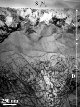
plasma-base ion implantation system described in previous papers [28,29]. The final microstructure is
illustrated with the TEM cross-sectional micrograph in Fig. 1: a compound layer (noted N)
consisting of nano-sized grains of titanium nitride lies at the surface, above a diffusion layer
(noted D) consisting of a solid solution of nitrogen in !-titanium with the same microstructure
as the initial substrate; the entire zone noted D in Fig. 1 is occupied by one !P nodule (the
high density of dislocations is due to tensile testing of the material before TEM observations).
The compound layer is about 500 nm thick and the diffusion layer a few micrometers thick
(the penetration of nitrogen depends on the crystallographic orientation of !-titanium grains
[29]). Note that an additional layer of amorphous Si3N4 lies above the compound layer.
[FIGURE 1]
TEM specimens were first machined using a diamond wire saw in the form of 0.5 x 1 x 3 mm
rectangles. The nitrided layer lies on one of the 3 mm length side of the rectangle. Samples
were then thinned down to a thickness of about 10-12 !m with SiC abrasive papers before
being glued to a copper support grid adapted to the TEM straining specimen holder.
Final thinning of the cross-section was then performed with Ga ions in a dual-beam FIB
(Zeiss 1540 equipped with an Orsay Physics multiple source ionic column), operating at an
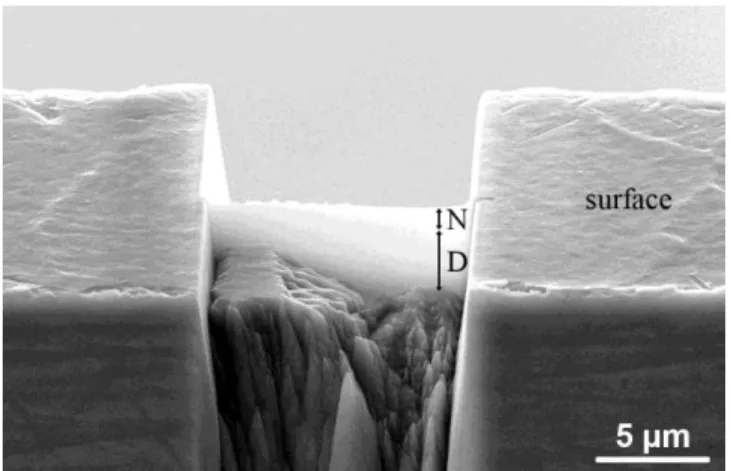
acceleration voltage of 30 kV. The H-bar design of the specimen is sketched in Fig. 2: an
electron transparent window is machined by ion milling in the middle of the top of the
specimen. Fig. 3 shows a scanning electron microscopy (SEM) view of the part of the
specimen containing the electron transparent area machined by FIB. Its dimensions are 12 !m
in width and about 5 !m in depth to allow observations of the entire nitrided zone (both
compound and diffusion layers). Its thickness is about 500 nm, sufficient to obtain electron
using a 150 pA ion beam current, followed by a 10 pA beam current polishing step. Note in
Fig. 3 that the top surface of the thinned part has been slightly damaged during ion milling,
but only the Si3N4 layer is partially removed and the nitrided surface remains damage-free.
The usual deposition of a Pt coating on the surface of the specimen was unnecessary here as
the Si3N4 layer protected the nitrided surface from the ion milling. The principle of this
method could be easily extended to other materials providing an adaptation of the thickness of
the pre-FIB foil and the final electron transparent window.
TEM in situ straining experiments were performed at 200 kV in a JEOL 2010 TEM equipped
with a video-rate Soft Imaging System CCD camera and using a Gatan straining holder.
[FIGURE 2]
[FIGURE 3]
3. Results and discussion
Fig. 4 (a) shows a low magnification TEM view of the electron-transparent zone of the
FIB-designed specimen prior to the in situ TEM straining experiment. Tensile direction lies
parallel to the surface along the horizontal direction of this figure. The compound layer is
visible on the top of the micrograph (denoted N). A nodule pertaining to the diffusion layer
lies below. This grain occupies almost the whole thinned area of the diffusion layer: the thin
part of interest where the plastic deformation was observed during testing is marked 1 and the
thicker part of this grain is noted 2. Fig. 4 (b) shows the same nodule after testing. Plastic
first direction is denoted A and forms an angle of about 45° with respect to the tensile
direction (horizontal direction). The second one, denoted B, is less contrasted than the first
one because of diffracting conditions and forms an angle of about 20° with respect to the
tensile direction.
[FIGURE 4]
Orientation of the slip traces along A in Fig. 4 (b) indicates that prismatic 1 1 0 0
{
}
glide is the first activated slip system and regular indexation method (g.b=0 conditions) shows thatdislocations have a-type 1 3 112 0 Burgers vectors (later called a-dislocations). The
individual motion of these dislocations was unfortunately difficult to observe because the
orientation of their slip planes lies nearly parallel to the electron beam direction. Nevertheless,
movements of several dislocations in the same plane were observed.
A second slip system was then activated: a-dislocations having the same Burgers vector
(1 3 112 0 ) than the previous slip system were observed to glide in first-order pyramidal
planes 1 0 1 1
{
}
. These dislocations did not cross-slip from the previous slip system. Their slip traces are very close to that of the previous slip system and correspond also to the tracesdenoted A in Fig. 4 (b): nevertheless, the two set of planes have a different angle with respect
to the surface of the thin foil and dislocations have thus a different shape depending on their
slip plane. The two slip systems can so be distinguished unambiguously and non-occurrence
of cross slip established. Fig. 5 shows an example of dislocations of this second slip system
with two dislocation loops (numbered 1 and 2) expanding in first-order pyramidal planes.
These dislocation loops are elongated along their screw direction. In these slip planes,
[FIGURE 5]
After a large activity of the two first slip systems, a third one with different a-dislocations was
observed. Dislocations glide in another set of 1 1 0 0
{
}
prismatic planes and form planar pile-ups as exemplified in Fig. 6: three dislocations, numbered 1, 2 and 3, are gliding together inthe same plane. Some dislocations have already slipped in this same plane. Slip traces of this
system are the traces denoted B in Fig. 4 (b).
The two first slip systems observed have Schmid factors (SFs) equal to 0.5 for the prismatic
system and equal to 0.46 to the pyramidal one. The third slip system activated has a SF equal
to 0.22. Note that no basal 0001
(
)
slip systems were observed according to their very low SF (<0.1) in this grain. Activation of these three slip systems is in agreement with previousobservations in the same alloy (without surface treatment): the first activated slip systems are
those with a-type dislocations gliding in prismatic or basal planes with the highest SF and
pyramidal slip systems can be activated if their SF is superior to about 0.46 [26,30]; in
addition, prismatic slip systems with really lower SF can sometimes be activated in already
deformed grains [30]. As the deformation modes are unaffected in comparison to the
macroscopic deformation of the material, one can conclude that:
- deformation modes are not modified by the specimen design and the preparation
process;
- deformation modes in the diffusion layer are not modified by the nitridation surface
treatment.
Moreover, present results show that screw segments of dislocations have a lower mobility
than non-screw segments in the diffusion layer. Thus, the deformation rate is governed by the
micromechanisms are then not drastically modified by nitridation in the diffusion layer. The
only difference between the deformation of the bulk alloy and the deformation of the
diffusion layer is that deformation seems more localized in this last one: deformation (in
prismatic planes) occurs in less numerous planes but with several dislocations in the same
plane. This could be due to a change of the chemical ordering in !P nodules of the diffusion
layer during the nitridation treatment [31]. Nevertheless, the hard compound layer is, as
expected, acting as a barrier to the propagation of dislocations. All these results have been
confirmed by post mortem TEM observations of previously deformed specimens and will be
discussed in a further work.
[FIGURE 6]
During the test, no evidence of plastic deformation in the compound layer was observed:
dislocations from the nodule below stopped at the interface between the two layers and did
not induce deformation in the compound layer. This confirms that this layer is much harder
than the alloy and can serve as an effective protective surface layer. Also, the absence of
crack nucleation during the experiment proved that the specimen design is appropriated to the
study of plastic deformation even in the presence of a fragile compound. Indeed, crack
initiation is often caused by surface damages in brittle materials. Those damages (micro
scratches, irregular shapes), which are hard to avoid in other methods such as standard low
angle ion milling for example [18,19] can be eluded with the precision of the focused ion
beam. Moreover, a protective layer (Pt, W) can be added in the FIB by ion-assisted
deposition.
From the total number of dislocations observed in the grain after the test, the local total
amount of plastic deformation, dislocations in the metallic material piled up against the brittle
material, but in insufficient quantity to provoke cracking or void formation. One can expect to
determine in situ the amount of plastic deformation in the metal layer necessary to cause the
nitride failure by piling up dislocations at the interface. We did not pursue the experiment to
that point.
4. Conclusions
A FIB-based method for the preparation of H-bar cross-sectional specimen for new in situ
TEM straining experiments was described and applied to a surface-nitrided titanium alloy.
The first in situ observations of dislocation motion in a metal/ceramic material were
performed to show the feasibility of the preparation route. This method proved time efficient
and robust to perform. It is applicable to a wide variety of materials and milling parameters,
dimensions and thickness of the electron-transparent window can be easily adapted to a
specific material. Others advantages include:
- Surface preservation and interface integrity. This point is crucial to prevent artificial
crack formation.
- Preservation of the metal properties and structure. This is favoured by the
perpendicular exposure to FIB damages that are blocked by the ceramic-type surface.
This was validated by the fact that the intrinsic deformation mechanisms in the
Ti-6Al-4V alloy were not modified by the design of specimen.
- Specific site inspection. As for most of FIB-based techniques, it is possible to choose
a specific observation site prior to final milling.
- The deformation mechanisms in the diffusion layer are almost the same than in the
bulk alloy, i.e. same dislocation type, same slip planes and a lower mobility of screw
segments.
- The compound layer remains undeformed and acts as a barrier to the propagation of
dislocations coming from the diffusion layer. This confirms the better resistance to
deformation (and thus wear) of the compound layer compared to the bare Ti alloy.
References
[1] G. Dehm, Prog. Mater. Sci. 54 (2009) 664-688.
[2] B.J. Inkson, G. Dehm, T. Wagner, Acta Mater. 50 (2002) 5033-5047.
[3] M. Legros, G. Dehm, T.J. Balk, Mater. Res. Soc. Symp. Proc. 875 (2005) 237-247.
[4] M. Legros, M. Cabie, D.S. Gianola, Microsc. Res. Tech. 72 (2009) 270-283.
[5] H. Saka, T. Kato, M.H. Hong, K. Kuroda, T. Kamino, In: Galvatech'95 Conference
Proceedings, Chicago (1995) 809–814.
[6] M.W. Phaneuf, Micron 30 (1999) 277-288.
[7] R.J. Patterson, D. Mayer, L. Weaver, M.W. Phaneuf, Microsc. Microanal. 8 (2002)
566-567.
[8] Z. Huang, J. Microsc. 215 (2004) 219-223.
[9] R.M. Langford, Microsc. Res. Tech. 69 (2006) 538-549.
[10] J. Li, T. Malis, S. Dionne, Mater. Charact. 57 (2006) 64-70.
[11] Y. Bhandari, S. Sarkar, M. Groeber, M.D. Uchic, D.M. Dimiduk, S. Ghosh, Comput.
Mater. Sci. 41 (2007) 222-235.
[12] B. Yao, K.R. Coffey, J. Electron Microsc. 57 (2008) 189-194.
[14] G. Dehm, M. Legros, B. Heiland, J. Mater. Sci. 41 (2006) 4484-4489.
[15] S.H. Oh, M. Legros, D. Kiener, P. Gruber, G. Dehm, Acta Mater. 55 (2007) 5558-5571.
[16] S.H. Oh, M. Legros, D. Kiener, G. Dehm, Nat Mater 8 (2009) 95-100.
[17] R.D. Field, P.A. Papin, Ultramicroscopy 102 (2004) 23-26.
[18] M.A. Wall, T.W. Barbee, Jr., T.P. Weihs, Microsc. Res. Tech. 36 (1997) 143-150.
[19] T. Foecke, D.E. Kramer, Int. J. Fract. 119 (2003) 351-357.
[20] U. Messerschmidt, M. Bartsch, C. Dietzsch, W. Kurtz, C. Scheu, M. Rühle, Z. Metallk.
95 (2004) 785-792.
[21] R. Morita, K. Azuma, S. Inoue, R. Miyano, H. Takikawa, A. Kobayashi, E. Fujiwara, H.
Uchida, M. Yatsuzuka, Surf. Coat. Technol. 136 (2001) 207-210.
[22] A. Tóth, M. Mohai, T. Ujvári, T. Bell, H. Dong, I. Bertóti, Surf. Coat. Technol. 186
(2004) 248-254.
[23] A.C. Fernandes, F. Vaz, E. Ariza, L.A. Rocha, A.R.L. Ribeiro, A.C. Vieira, J.P. Riviere,
L. Pichon, Surf. Coat. Technol. 200 (2006) 6218-6224.
[24] F. Foucher, C. Coupeau, J. Colin, A. Cimetiere, J. Grilhe, Phys. Rev. Lett. 97 (2006)
096101.
[25] P. Villechaise, X. Milhet, B. Angleraud, V. Fouquet, L. Pichon, A. Straboni, P.Y.
Tessier, Thin Solid Films 482 (2005) 324-329.
[26] P. Castany, F. Pettinari-Sturmel, J. Crestou, J. Douin, A. Coujou, Acta Mater. 55 (2007)
6284-6291.
[27] P. Castany, F. Pettinari-Sturmel, J. Douin, A. Coujou, Mater. Sci. Eng., A 483-484
(2008) 719-722.
[28] J. Perrière, J. Siejka, N. Remili, A. Laurent, A. Straboni, B. Vuillermoz, J. Appl. Phys.
59 (1986) 2752-2759.
[30] F. Bridier, P. Villechaise, J. Mendez, Acta Mater. 53 (2005) 555-567.
Fig. 1. Cross-sectional TEM view of the nitrided Ti-6Al-4V alloy showing the compound layer (noted N) and a part of the diffusion layer (noted D). The amorphous Si3N4 deposit lying
on the nitrided surface is also observable. This sample was thinned with a standard ion milling procedure using a Gatan PIPS.
Fig. 2. Sketch of the shape of the in situ TEM cross-sectional specimen. The electron transparent window is made by FIB. Thick arrows indicate the direction of tensile strain. N represents the nitride layer thickness (displayed in light grey).
Fig. 3. SEM image of the electron transparent window machined with FIB and sketched in the previous figure. N indicates the compound layer thickness and D the diffusion layer one.
Fig. 4. TEM views of the electron transparent zone before (a) and after (b) the straining experiment (diffraction conditions close to [0002] zone axis). The compound layer is denoted N. The thinned part of the grain of the diffusion layer observed during testing is denoted 1 and a thicker part is denoted 2. Two slip trace directions forming an angle of about 60° (A and B) are visible.
Fig. 5. In situ TEM sequence showing dislocations with a-type Burgers vectors expanding in first-order pyramidal planes.
Fig. 6. In situ TEM sequence showing a-type dislocations piling up in a prismatic plane.

![Fig. 4. TEM views of the electron transparent zone before (a) and after (b) the straining experiment (diffraction conditions close to [0002] zone axis)](https://thumb-eu.123doks.com/thumbv2/123doknet/13663170.429783/17.892.300.593.100.780/views-electron-transparent-straining-experiment-diffraction-conditions-close.webp)


