HAL Id: hal-01659180
https://hal.laas.fr/hal-01659180
Submitted on 8 Dec 2017HAL is a multi-disciplinary open access archive for the deposit and dissemination of sci-entific research documents, whether they are pub-lished or not. The documents may come from teaching and research institutions in France or abroad, or from public or private research centers.
L’archive ouverte pluridisciplinaire HAL, est destinée au dépôt et à la diffusion de documents scientifiques de niveau recherche, publiés ou non, émanant des établissements d’enseignement et de recherche français ou étrangers, des laboratoires publics ou privés.
Extended Defects Formation in Nanosecond
Laser-Annealed Ion Implanted Silicon
Yang Qiu, Fuccio Cristiano, Karim Huet, Fulvio Mazzamuto, Giuseppe
Fisicaro, Antonino La Magna, Maurice Quillec, Nikolay Cherkashin, Huiyuan
Wang, Sébastien Duguay, et al.
To cite this version:
Yang Qiu, Fuccio Cristiano, Karim Huet, Fulvio Mazzamuto, Giuseppe Fisicaro, et al.. Extended Defects Formation in Nanosecond Laser-Annealed Ion Implanted Silicon. Nano Letters, American Chemical Society, 2014, 14 (4), pp.1769-1775. �10.1021/nl4042438�. �hal-01659180�
Extended defects formation in nanosecond
laser-annealed ion implanted silicon
Yang Qiu,† Fuccio Cristiano,*,† Karim Huet, ‡ Fulvio Mazzamuto, ‡ Giuseppe Fisicaro§, Antonino La Magna, § Maurice Quillec,ǁ Nikolay Cherkashin, †† Huiyuan Wang, ‡‡ Sébastien Duguay, ‡‡ and Didier Blavette‡‡
† LAAS, CNRS and Université de Toulouse, 7 av. Du Col. Roche, 31400 Toulouse, France ‡ Excico, 13-21 Quai des Gresillons, 92230 Gennevilliers, France
§ CNR-IMM, VIII Strada, I-95121 Catania, Italy
ǁ Probion Analysis, 37 rue de Fontenay, 92220 Bagneux, France
†† CEMES, CNRS UPR 8011 and Université de Toulouse, 29 rue Jeanne Marvig, 31055
Toulouse, France
ABSTRACT Damage evolution and dopant distribution during nanosecond laser thermal annealing of ion implanted silicon have been investigated by means of transmission electron microscopy, secondary ion mass spectrometry and atom probe tomography. Different melting front positions were realized and studied: non-melt, partial melt and full melt with respect to the as-implanted dopant profile. In both boron and silicon implanted silicon samples, the most stable form among the observed defects is that of dislocation loops lying close to (001) and with
Burgers vector parallel to the [001] direction, instead of conventional {111} dislocation loops or {311} rod-like defects, which are known to be more energetically favourable and are typically observed in ion implanted silicon. The observed results are explained in terms of a possible modification of the defect formation energy induced by the compressive stress developed in the non-melted regions during laser annealing.
KEYWORDS: laser thermal annealing, extended defects, transmission electron microscopy, secondary ion mass spectrometry, atom probe tomography, ion implantation.
Laser Thermal annealing (LTA) of ion implanted silicon in the nanosecond regime has attracted a considerable attention as it has been recognized as a promising candidate for numerous state-of-the-art semiconductor applications. Such an ultra-fast, localized and low thermal budget treatment (including both non-melt and melt conditions) has already shown its ability to effectively activate ion implanted dopants, e.g. boron, restrained to a very thin layer near the surface without harming the underlying buried device layers, which is of critical importance for 3D integrated devices, including BackSide Illuminated CMOS Imaging Sensors (CIS) and power devices.1-3
Previous studies over the last decades have demonstrated that during conventional (furnace) and rapid thermal annealing (RTA), such as spike-RTA and flash-RTA, excess Si interstitials created by ion implantation precipitate in the form of small clusters continuously transforming into different types of extended defects that evolve following an Ostwald ripening mechanism. In addition, their effect on transient enhanced diffusion (TED)4-5 and deactivation of dopants6 have been established. The crystallographic characteristics of these extended defects ({311} or {111} rod-like defects and {111} dislocation loops (DLs)), named hereafter “conventional” defects, have been reported.5,7 {111} DLs exhibit Burgers vectors lying along <111> directions (Faulted DLs) or <110> directions (Perfect DLs). In addition, “unconventional” DLs with the (001) habit plane and Burgers vector lying along the [001] direction have also been observed in the past in the presence of high concentrations of boron (above its solid solubility in Si)8-10. These loops are formed in the early stages (i.e. after few seconds anneal at low temperature) of boron and Si interstitials co-precipitation and are known as “large” boron interstitial clusters (BICs). In contrast, the much shorter duration time of excimer laser annealing (<200 ns) is comparable to that of some basic point-defect related phenomena, such as Si interstitial diffusion and
clustering11, which makes the defect-formation mechanism itself questionable in this annealing regime. In addition, most of the existing studies of defect formation in laser annealed silicon have been carried out in preamorphised structures: (i) after non-melt anneals, conventional end-of-range defects ({311} defects and {111} DLs) have been observed12-14; (ii) in the case of melt laser annealing, the defects nature depends on the position of the melt front with respect to the amorphous/crystalline, a/c, interface (stacking faults are observed in the case of incomplete melting of the preamorphised layer,15 defect-free crystalline silicon is found when melting goes beyond the a/c interface16).
Recently, various applications1-3 have been demonstrated, in which laser annealing is performed in structures implanted with non-amorphising implants. Non-amorphising implants are
characterised by a much wider point defect distribution compared to amorphising implants, allowing for a more fundamental investigation of the damage formation as a function of the location of the melt front vs. the point defect distribution. However, no investigations have been carried out for these technologically relevant conditions.
In this work, we present an experimental characterisation of the extended defects formed in silicon after non-amorphising ion implantation and laser annealing, using specific transmission electron microscopy (TEM) techniques together with secondary ion mass spectroscopy (SIMS) and atom probe tomography (APT). Instead of “conventional” Si interstitial defects, DLs with Burgers vector, b, parallel to [001] are found to be the most stable form in both boron and silicon implanted silicon. The observed results are discussed in terms of the modification of the defect formation energy induced by the compressive stress developed in the non-melted regions during laser annealing.
Two CZ (001) Si wafers (200 mm, n-type) were implanted respectively with 30 keV B+ ions to a nominal dose of 1×10¹⁵ ions/cm2 and 80 keV Si+ ions to a nominal dose of 2.75×10¹⁴ ions/cm2. Both the energy and dose were selected using Stopping and Range of Ions in Matter (SRIM) simulations17 in order to achieve a comparable dopant and point defects (Si interstitials and vacancies) depth distribution after the implant: the impurity projected range, Rp, is located at a
depth close to 100 nm while the maximum estimated defect concentration is located at about 80 nm. Several square areas (18x18 mm2) of the implanted wafers were laser annealed using the Excico Excimer LTA system based on UV radiation (λ=308 nm, pulse duration < 200 ns), with laser energy densities (ED) ranging from 1.5 J/cm2 to 2.9 J/cm2 and different numbers of pulses (from 1 to 10). These conditions allowed to investigate different regimes of the Excimer Laser annealing process, including non-melt (10 pulses of 1.5 J/cm2), for which the surface temperature reaches around 1400 ⁰C for about 100 ns without melting, partial melt with melted depth not reaching the peak of the point defect profile, (1 pulse of 2.3 J/cm2), partial melt with melted depth beyond the peak of the point defect profile (1 pulse of 2.6 J/cm2) and full melt (1 pulse of 2.9 J/cm2) of the implanted profile.
Boron concentration profiles were analysed by SIMS using CAMECA IMS-4F and 7F systems. Both plan-view (PV) and cross-sectional (CS) TEM specimens were prepared by standard methods involving cutting, gluing, polishing, dimple grinding and Ar+ ion milling until perforation. Plan-view TEM analysis was performed on a JEOL 2010-HC system available at CEMES-CNRS, Toulouse, using weak-beam dark-filed (WBDF) imaging conditions with various diffracting vectors, g. Cross-sectional WBDF images with g = [004] and high resolution TEM images were taken by using a JEOL JEM 2100F transmission electron microscope with field emission gun (TEM-FEG) operating at 200 kV, available at the TEMSCAN service of the
University Paul Sabatier of Toulouse. Several CS TEM specimens were prepared by tripod polishing only to be studied by geometric phase analysis (GPA) of HRTEM images. The experiments were performed at 200 kV at the spherical aberration corrected FEI-Tecnai SACTEM-Toulouse microscope located in CEMES-CNRS Toulouse. Finally, APT analyses were performed using a CAMECA LAWATAP instrument with an amplified ytterbium doped laser at a wavelength of 343 nm with an energy of 35 nJ/pulse providing a 350 fs pulse duration, spot size of 100 µm, and 100 kHz repetition rate.
Boron concentration profiles measured by SIMS for four different laser annealing conditions are reported in Fig. 1. Each profile is superimposed on the corresponding cross-sectional TEM image. In the non-melt case (1.5 J/cm2), no change in the dopant profile was observed compared to the as-implanted one (not shown), even with multiple pulse conditions (10 pulses case shown in Fig. 1a). In the case of partial melt with melted depth not reaching the peak of the point defect profile (2.3 J/cm2, Fig. 1b), a redistribution of the dopant is observed, with the appearance of a quasi-plateau in the melted region (the liquid/solid, l/s, interface is indicated by a white dotted line) and a depletion near the surface. These two features are more evident in the samples annealed with higher energy density (Fig. 1c-d) which also exhibit a dopant pile-up just below the l/s interface. All of the observed features are typical of boron profiles obtained after ion implantation and melting excimer laser annealing and can be well explained as a consequence of dopant adsorption at the solid-liquid interface during solidification.18,19
The cross-sectional WBDF TEM images, also reported in Fig. 1 and obtained using the [004] diffraction vector, g, show the location of the observed extended defects, which is directly correlated with the corresponding boron distribution profile. The majority of the visible defects are distributed in the range specified by the red lines reported in each figure. TEM image of the
non-melt sample (1.5 J/cm2) indicates that the visible defects occupy a wide region extending from the surface down to a depth of about 160 nm. The defect region is centered on the projected range of the implanted boron. This is in agreement with the consideration that, during annealing in the solid phase, the defects are expected to form in a region containing the maximum amount of impurity and excess interstitial atoms, i.e. in a relatively wide region centered at the boron projection range, Rp. TEM images of partially melt samples with melted depth above (Fig. 1b)
and below (Fig. 1c) the peak of the point defect profile reveal that the observed defects are located in a region extending from ~75 to ~185 nm and from ~135 to ~175 nm, respectively. The upper limit of the defect regions correspond to the thickness of the liquid layer created during laser annealing in both cases. Therefore, the observed defects are formed in the solid phase just below l/s interface. Indeed, high temperatures (in the range of 1400°C) are reached during annealing in this region, so that the residual point defects and implanted impurities present there can precipitate in the form of extended defects, whose nature is discussed below. In addition, the apparent defect size (up to ~10 nm in the upper limit of the defect layer) decreases with
increasing depth. This result is in agreement with the rapid decrease of the substrate temperature below the melted region20,21, as shown in the inset of Fig. 1d, where the depth variation of the peak temperature reached during laser annealing at 2.6 J/cm2 was calculated following the phase-field methodology.34 Finally, no defects are observed in the sample with a melted region
extending well beyond the peak of the point defect profile (2.9J/cm2, Fig. 1d, i.e. no implant-induced point defects are left in the non-melted region).
The nature of the observed defects has been initially investigated using the g·b defect contrast method, which allows the determination of the Burgers vector direction, b, with g being the diffracting vector used for TEM imaging. For this, plan-view specimens were used. Figure 2
depicts plan-view TEM images of the observed samples (1 per each row) using different diffraction vectors, g (1 per each column). For each sample, the first two images from the left, were taken with the electron beam perpendicular to the (001) wafer surface, i.e. using the [00-1] zone axis, with g=<220> and <040>, respectively. The rightmost image in each case was taken in the tilted beam configuration, namely the [1-1-3] zone axis, with g = [2-42] or [-42-2], as specified in the figure. Independently of the laser energy density and number of pulses, it was found that all observed defects exhibit a loop-like contrast, as shown in the insets of the images taken from the sample annealed with 1.5 J/cm2 (Fig. 2, 1st row left and 1st row right). The absence of {311} rod-like defects is in agreement with the extremely high temperatures (~1400°C) reached in the solid phase just below the l/s interface (in the case of melt laser conditions) or below the surface (in the non-melt laser condition).
If the observed loops were conventional {111} interstitial loops (perfect loops with b//<110> and faulted loops with b//<111>), the number of defects with strong inside contrast had to slightly increase when moving from perpendicular (the [00-1] zone axis) to tilted beam (the [1-1-3] zone axis) imaging configuration, which should result in a slight increase of the visible defect density. In contrast, in all the annealed samples investigated in this work, the visible defect density significantly increases when using the [1-1-3] zone axis compared to the [00-1] one, as shown by the TEM micrographs of Fig. 2 (3rd column). In particular, very few defects appear in the first two images of the sample annealed with a laser energy of 2.6 J/cm2 (bottom row in Figure 2). However, the image taken with g= [-42-2] exhibits the presence of a high density of defects with the loop like contrast, suggesting that an additional loop family is present in these samples, with aBurgers vector parallel to the [001] direction and a habit plane parallel to the (001) surface, as indicated by HREM analysis (cf Fig. 3a and Fig. 3b). Indeed, such loops would exhibit no
contrast in images taken in the [00-1] zone axis (g.b=0) while being visible in the [1-1-3] zone axis (g.b≠0).
Based on these considerations, a quantitative method based on the variation of the apparent defect density in plan-view WBDF TEM images (c.f. fig. 2) with changing diffracting vector has been used to estimate the density of the various possible defect types according to their Burgers vector (<111>, <110> or [001]). The results clearly indicate that the vast majority of defects in these samples consist of (001) DLs, whose relative fraction increases from about 60% in the sample annealed with 2.3 J/cm2 laser energy, up to almost 100% in the sample annealed with a laser energy of 2.6 J/cm2. In addition, the total density of observed defects (of the order of ~1x1011 cm-2) is found to decrease when the laser energy density is increased. Indeed, the width of the molten region increases proportionally to the thermal budget, which results in a reduced concentration of residual point defects (and dopant impurities) available for defect formation in the non-melted region22. In order to further confirm that (001) loops are indeed formed in the observed samples, a more detailed analysis was performed using Geometric Phase Analysis (GPA)9 of cs(110) HRTEM images of the sample annealed with 2.6 J/cm2 (1 pulse, cf. Fig.3). Figures 3a and 3b show the HRTEM images of an area containing a loop seen in edge-on position, i.e. with its habit plane being perpendicular to the image plane, and the enlarged image of the defect itself, respectively. The images clearly show that the defect consists of an additional plane of atoms parallel to the (001) plane, as pointed by the two white arrows, i.e. it is of
extrinsic type. After Fourier transform of the original HREM image, the phase images P002 and
P220, corresponding to the 002 and 220 Fourier spots, are calculated, and shown in Figures 3c
and 3d, respectively. These phase images describe the projection of the defect induced displacement field in the image plane and allow to extract the projection of the DL Burgers
vector in the image plane following the procedure described in [9] It is found that no phase variation is observed across the defect in the phase image relative to the [110] direction, P220,
while a clear phase jump of about 2.5 rad is seen in the perpendicular P002 image (c.f. the inset of
Fig. 3c), therefore confirming that the observed loops have a Burgers vector parallel to the [001] direction. In addition, the GPA method gives direct evidence for the sense of the
corresponding atomic plane displacements around the defect, allowing to further confirm that the defect is of extrinsic type, i.e. it contains an additional plane of interstitials. Finally, following the calculation method described in [23,24], it is also possible to estimate the
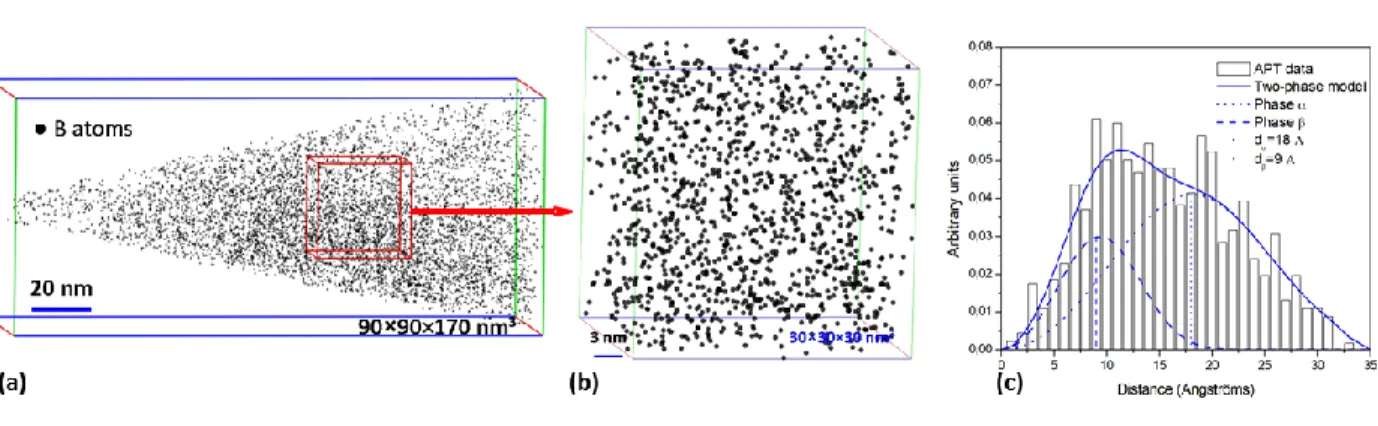
amplitude of the Burgers vector of these dislocation loops, which is found to be ~1/4 [001]. Large loops lying on (001) planes with Burgers vector parallel to the [001] direction, have already been observed in silicon implanted with high boron doses (above solid solubility).8,25 These loops are known as “Large BICs” and their formation occurs during the early stages of boron and Si interstitials co-precipitation, as confirmed by Atom Probe analyses in a previous work10. However, in the samples investigated here, the maximum boron concentration is well below the solid solubility limit26 and no precipitation is expected during annealing. In order to clarify this point, APT analysis was carried out on the sample annealed with 2.6 J/cm2. The APT reconstruction is presented in Fig. 4a, where boron atoms are shown as black dots. The
reconstruction was calibrated in depth using the SIMS profile. A selected volume in the region containing the (001) loops has been magnified in Fig. 4b. No clusters such as B-rich platelets (i.e. Boron precipitates)10 or (001) loops decorated by B atoms27 can be directly evidenced from the image. This is further confirmed after applying, to the same volume of several analyzed specimens, a quantitative statistical method specifically developed for the investigation of Boron clustering and based on the distance distribution between the first nearest neighbors atoms28 (Fig.
4c). The asymmetric shape of the distribution reveals that boron atoms are not homogeneously distributed within the defect region, indicating that some short range ordering exists between B atoms. More precisely, there is a clustering trend (more B-B pairs than expected in a random solid solution), however a well-defined clustered phase is not identified.
The role of boron in the formation of the observed defects seems to be different from that observed in previous works10. In order to assess a possible chemical effect of the presence of B atoms on the structure of the observed defects, Si-implanted samples (i.e. without any boron) were therefore laser annealed and analyzed by TEM. Although the Si+ and B+ implant conditions were chosen in order to achieve a comparable dopant and point defects (Si interstitials and vacancies) depth distribution after the implant, TEM observation of the as-implanted samples (not shown) indicated that the Si+ implant created more damage compared to the B+ one, with the former showing the presence of isolated amorphous pockets. In addition, TEM observations after laser annealing show that the melting depth at a given energy density (visible defect band) is about 40-50 nm smaller in the Si+ implant case. This is thought to be due to a difference in the surface reflectivity linked to the absence of boron in the Si implant sample29. Moreover, the higher damage density in the Si+ implant case may influence the local melt temperature, which in turn may impact the melt depth at a given energy density. However, it is important to note that these differences are not expected to affect the relevance of the investigation of the defect nature formed during laser annealing, which is the main objective of this study.
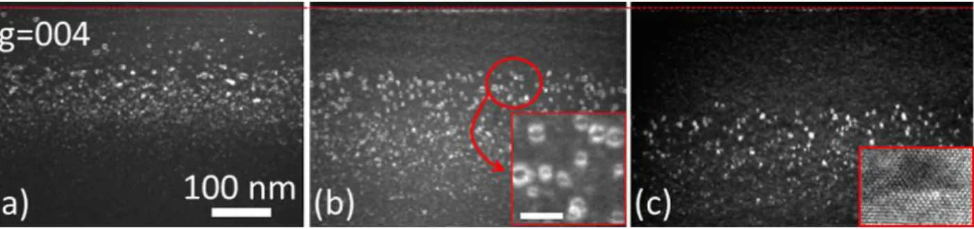
Fig. 5 compares different laser-annealed Si+- implanted samples using CS WBDF images taken with the diffraction vector, g = [004]. Apart from the differences highlighted above, the defect location is again directly related to the laser melt/non-melt conditions. In the case of a non-melt
some of them being located just below the surface. In contrast, for the Si+ implanted sample laser-annealed at 2.6 J/cm² (Fig. 5b), the surface region is defect free down to a depth of about 100 nm, corresponding to the thickness of the melted region. As in the B+ case, the apparent defect size in the defect layer, located below the l/s interface, decreases with increasing depth. Finally, for the Si+ implanted sample laser-annealed at 2.9 J/cm² (Fig. 5c), defects can still be observed, unlike the corresponding B+ implanted sample annealed with the same energy density, in agreement with the higher damage created during the Si+ implant. Again, the defect layer starts below the depth of the l/s interface (~160 nm below the surface), with a defect size distribution similar to that of the sample annealed with 2.6 J/cm² (maximum apparent size: ~ 10 nm).
It is important to note that, similarly to the B+ implant case, all of the observed defects exhibit a loop-like contrast, as evidenced by the inset of Fig. 5b as well as by HREM images, with several loops lying on (001) planes (cf. inset of Fig. 5c). In addition, according to the g·b defect contrast method and GPA analysis (images not shown), the presence of (001) loops with Burgers vector parallel to [001] has also been confirmed. Indeed, independently of the laser energy density, the number of visible defects in the tilted beam configuration ([1-1-3] zone axis) is much higher than in the case of a beam perpendicular to the (001) surface. In particular, no defects were observed when using an electron beam perpendicular to the (001) surface in the sample annealed with 2.9 J/cm², indicating that the totality of the existing defects in this sample are (001) DLs having Burgers vector lying along the [001] direction (their fraction reduces to 80 % in the sample annealed with 1.5 J/cm2 laser energy). Besides, the total density of observed defects (~3x1011 cm-2 in the sample annealed with 1.5 J/cm2) is found to decrease by a factor 10 when the thermal budget is increased to 2.9 J/cm².
After melt or non-melt laser annealing of (001) Si implanted either with B+ or Si+ ions under non-amorphising conditions, the majority of the defects formed in the non-melted region take the form of (001) loops instead of conventional {111} dislocation loops or {311} rod-like defects, which are known to be more energetically favourable, according to calculations of the formation energy30-32. These loops are systematically located below the maximum liquid/solid interface depth and have been observed not only in the LTA boron implanted samples but also in the LTA silicon implanted samples. Therefore, despite being similar in nature to the “Large BICs”
observed in high-dose B+-implanted Si (i.e. Boron precipitates), the defects formed here are not “large BICs” but would rather be large Si interstitial (001) loops potentially decorated by boron atoms (in the B implanted cases).
A possible explanation of the observed results can be proposed considering that the defect formation energy can be modified in the presence of external stress33-34. In particular, for a bi-axial stress in the x-y plane parallel to the surface, (i) the modification of the defects formation energy value is proportional to the projection of the defect Burgers vector in the (001) plane and to the applied stress; (ii) the formation energy of extrinsic type defects, such as those investigated in this work, increases (decreases) in the presence of a compressive (tensile) stress. An important consequence of this effect is that the stress does not modify the formation energy of the defects with Burgers vector perpendicular to the stress plane. Indeed, in previous works35, we have already observed the suppression of some variants of {311} rod-like defects in tensile strained Si, which was explained assuming a stress-induced modification of the {311}s formation energy.
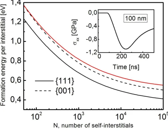
In the case investigated here, it is speculated that, during laser annealing, the strong temperature gradients existing between the solid (crystalline) region immediately below the free surface (in the case of non-melting process) or the l/s interface (in the case of a melting process) and the deeper substrate regions result in a depth-dependent lattice parameter modification and a corresponding compressive biaxial stress field. As an example, the inset of Fig. 6 shows the stress variation as a function of annealing time calculated at a depth of 100 nm for the “non-melt” laser annealing case (i.e. 1.5 J/cm2) at a temperature just below the melting threshold. The calculation was made coupling the phase-field methodology36 for the simulation of the
temperature T and phase fields with the thermo-elastic theory, where the constitutive relations
kl kl(T T0)
ij
E , relating the stress , strain and thermal fields, are calibrated with
the c-Si elastic constants tensor E and expansion coefficient . Here, zero stress conditions are imposed for the stress components zz normal to the free boundary (i.e the free surface or the l/s
interface). A maximum compressive stress xx (or yy) of ~1 GPa is estimated after 200 ns.
According to the model mentioned above, such compressive stress has no impact on the formation energy of (001) loops (Burgers vector perpendicular to the stress plane). In contrast, the formation energy of conventional defects ({111} dislocation loops or {311} rod-like defects), increases under the applied stress. Figure 6 reports the formation energy of both conventional {111} and “unconventional” (001) dislocation loops as a function of defect size in the absence of an external stress field (black lines). As expected, being more energetically favourable, the formation energy of {111} loops is systematically lower than that of (001) loops. However, when calculated at the time of maximum compressive stress, the formation energy of {111} loops (red curve in Fig. 6) overcomes that of (001) loops. The latters might therefore become the
most favourable defect configuration during ultra-fast laser annealing, in agreement with the results found in the investigated samples.
In summary, we have investigated the defect formation in B+ or Si+ implanted Silicon following LTA in both non-melt and melt conditions. Different melting front positions (with respect to the as-implanted dopant depth distribution) were realized and studied: non-melt, partial melt and full melt. We found that the majority of the formed defects take the form of (001) loops instead of conventional {111} dislocation loops or {311} rod-like defects, which are known to be more energetically favourable. These loops are systematically located below the maximum l/s interface depth and have been observed not only in the LTA boron implanted samples but also in the LTA silicon implanted samples. Therefore, despite being similar in nature to the “Large BICs”
observed in high-dose B+-implanted Si (i.e. Boron precipitates), the defects formed here are not “large BICs” but would rather be large Si interstitial (001) loops potentially decorated by boron atoms (in the B implanted cases). The observed results are explained in terms of the modification of the defect formation energy induced by the compressive biaxial stress developed in the non-melted regions during laser annealing.
Figure 1. SIMS boron profiles and corresponding cross-section TEM images from B implanted
samples annealed by (a) 10 pulses at 1.5 J/cm2 (non-melt), (b) 1 pulse at 2.3 J/cm2 (partial melt above the Rp), (c) 1 pulse at 2.6 J/cm2 (partial melt beyond the Rp) and (d) 1 pulse at 2.9 J/cm2
(full melt). Inset: Calculated depth variation of the peak temperature reached during laser annealing at 2.6 J/cm-2.
Figure 2. Plan-view WBDF TEM images of B implanted samples annealed by (top row) 10
pulses at 1.5 J/cm2 (non-melt), (middle row) 1 pulse at 2.3 J/cm2 (partial melt above the Rp),
(bottom raw) 1 pulse at 2.6 J/cm2 (partial melt beyond the Rp). Images are taken using different
zone axes and diffracting vectors. Left column: Z.A.: [00-1], g=<220>; Middle column: Z.A.: [00-1], g=<400>; Right column: Z.A.: [1-1-3], g=<422>.
Figure 3. Geometric phase analysis of a dislocation loop in a B implanted sample annealed by 1
pulse at 2.6J/cm2. (a) HRTEM image in [-110] orientation; (b) enlarged view of the dislocation. The habit plane is (001); (c) geometric phase image of the 002 lattice fringes; (d) geometric phase image of the 220 lattice fringes.
Figure 4. (a) Atom probe tomography (APT) analysis of the boron implanted sample annealed
with 2.6 J/m2, (b) a volume is selected in the region below the l/s interface where the (001) loops are observed, (c) distribution of the first nearest neighbor (1NN) distances between B atoms in the selected volume of two samples. The distribution is fitted with a two phase model (solid line). Dotted and dashed lines represent the distributions related to the α (dα=18 Ǻ, solid
Figure 5. Cross section WBDF TEM images (surfaces are indicated by the red dashed line) of
the Silicon implanted sample annealed by (a) 10 pulses at 1.5 J/cm2 (non-melt), (b) 1 pulse at 2.6 J/cm2 (partial melt above Rp). Scale bar in the inset is 20 nm, (c) 1 pulse at 2.9 J/cm2 (partial melt
Figure 6. Inset: stress variation as a function of annealing time calculated at a depth of 100 nm
for a laser annealing at a temperature just below the melting threshold. A maximum biaxial compressive stress of ~1 GPa is estimated after 200 ns. Main plot: formation energy of
conventional {111} and “unconventional” (001) dislocation loops (black curves) as a function of defect size in the absence of an external stress field. When calculated at the time of maximum compressive stress, the formation energy of {111} loops (red curve) increases and overcomes that of (001) loops.
AUTHOR INFORMATION
Corresponding Author
* E-mail: [email protected]
Author Contributions
The manuscript was written through contributions of all authors. All authors have given approval to the final version of the manuscript.
ACKNOWLEDGMENT
F.C. wishes to thank A. Claverie for inspiring discussions. The research leading to these results received funding from the European Union Seventh Framework Programme (FP7/2007-2013) under grant agreement n° 258547 (ATEMOX).
DISCLOSURE STATEMENT
REFERENCES
1 M. Rahimo, C. Corvasce, J. Vobecky, Y. Otani, and K. Huet, IEEE Electron device lett. 33, 1601 (2012)
2 K. Huet, C. Boniface, R. Negru, and J. Venturini, in ion implantation technology 2012: proceedings of the 19th international conference on ion implantation technology (IIT), Valladolid, Spain, 25-29 June 2012, edited by L. Pelaz, I. Santos, R. Duffy, F. Torregrosa and K. Bourdelle (AMER INST Physics, New York, 2012), pp. 135-138
3 J. Venturini, in Junction Technology (IWJT) 2012: proceedings of the 12th International Workshop on Junction Technology, Shanghai, China, 14-15 May 2012, pp. 57-62
4 S. C. Jain, W. Schoenmaker, R. Lindsay, P. A. Stolk, S. Decoutere, M. Willander, and H. E. Maes, J. Appl. Phys. 91, 8919 (2002)
5 A. Claverie, B. Colombeau, B. De Mauduit, C/ Bonafos, X. Hebras, G. Ben Assayag, and F. Cristiano, Appl. Phys. A 76, 1025 (2003)
6 B.J. Pawlak, R. Surdeanu, B. Colombeau, A.J. Smith, N.E.B. Cowern, R. Lindsay, W. Vanderrvorst, B. Brijs, O. Richard, F. Cristiano, Appl. Phys. Lett. 84 (2004) 2055
7 S. Boninelli, N. Cherkashin, A. Claverie and F. Cristiano, Appl. Phys. Lett. 89 (2006) 161904
8 F. Cristiano, X. Hebras, N. Cherkashin, A. Claverie, W. Lerch, and S. Paul, Appl. Phys. Lett. 83, 5407 (2003)
9 N. Cherkashin, M. Hytch, F. Cristiano, and A. Claverie, Solid State Phenomena 108-109, 303 (2005)
10 O. Cojocaru-Mirédin, F. Cristiano, P.-F. Fazzini, D. Mangelinck, and D. Blavette, Thin Solid Film 534, 62 (2013)
11 H. W. Kennel, M. D. Giles, M . Diebel, P. H. Keys, J. Hwang, S. Govindaraju, M. Liu, and A. Budrevich, in Advanced Thermal Processing of Semiconductors 2006: proceedings of 14th IEEE International Conference, Kyoto, Japan, 10-13 October 2006, pp. 85-91
12 S. Earle, M. Law, R. Brindos, K. Jones, S. Talwar, and S. Corcoran, IEEE transactions on electron devices 49, 1118 (2002)
13 J. A. Sharp, N. E. B. Cowern, R. P. Webb, K. J. Kirby, D. Giubertoni, S. Gennaro, M. Bersani, M. A. Foad, F. Cristiano, and P. F. Fazzini, Appl. Phys. Lett. 89, 192105 (2006) 14 J. A. Sharp, A. J. Smith, R. P. Webb, K. J. Kirkby, N. E. B. Cowern, D. Giubertoni, S.
Gennaro, M. Bersani, M. A. Foad, P. F. Fazzini, and F. Cristiano, Appl. Phys. Lett. 92, 082109 (2008)
15 Y. Takamura, P. B. Griffin, and J. D. Plummer, J. Appl. Phys. 92, 235-244 (2002)
16 K. S. Jones, E. Kuryliw, R. Murto, M. Rendon, and T. Somit, in ion implantation technology 2000: proceedings of the 2000 international conference on ion implantation technology (IIT), Alpbach, Austria, 17-22 September 2000, pp. 111-114
18 M. Hackenberg, P. Pichler, K. Huet, R. Negru, J. Venturini, G. Fisicaro, A. La Magna, Proc. Of the 19th Ion Implantation Technology Conference, AIP conf. proc. 1496 (2012) 241 19 G. Fisicaro, K. Huet, R. Negru, M. Hackenberg, P. Pichler, N. Taleb, and A. La Magna,
Phys. Rev. Lett. 110, 117801 (2013)
20 M. Hackenberg, P. Pichler, K. Huet, R. Negru, J. Venturini, A. Pakfar, C. Tavernier, A. La Magna., Appl. Surf. Sci. 28, 9347 (2012)
21 G. Fisicaro, L. Pelaz, P. Lòpez, and A. La Magna Phys. Rev. E 86, 036705 (2012)
22 Defect density reduction with increasing thermal budget might also be expected as a consequence of Ostwald ripening. However, the timescale associated to laser annealing, is too short to support this explanation. In addition, no significant increase in defect size (an additional consequence of Ostwald ripening) is observed in these samples when the thermal budget is increased.
23 M.J. Hytch, J.L. Putaux, J.M. Pénisson, Nature 423, 270-273 (2003)
24 N. Cherkashin and A. Claverie, “Characterisation of process induced defects”, in “Transmission Electron Microscopy in Microelectronics”, A. Claverie ed., p. 165-197, Wiley (2013)
25 S. Boninelli, S. Mirabella, E. Bruno, F. Priolo, F. Cristiano, A. Claverie, D. De Salvador, G. Bisognin and E. Napolitani, Appl. Phys. Lett. 91, 031905 (2007)
26 S. Solmi, E. Landi, and F. Baruffaldi, J. Appl. Phys. 68, 3250-3258 (1990)
28 T. Philippe, M. Grubera, F. Vurpillot and D. Blavette, Microscopy and Microanalysis 16 (2010) 643
29 G. E. Jelllison, S. P. Withrow, J. W. McCamy, J. D. Budai, D. Lubben, and M. J. Godbole, Phys. Rev. B 52, 14607-14614 (1995)
30 J.P. Goss, T.A.G. Eberlein, R. Jones, N. Pinho, A.T. Blumenau, T. Frauenheim, P.R. Briddon, and S. Oberg, J. Phys.-Condes. Matter 14 (2002) 12843
31 J.P. Goss, P.R. Briddon, T.A.G. Eberlein, R. Jones, N. Pinho, A.T. Blumenau, and S. Oberg, Appl. Phys. Lett. 85 (2004) 4633
32 T.A.G. Eberlein, Point and Extended Defects in Group IV Semiconductors, PhD Thesis, University of Exeter, 2004
33 A.J. Pitera and E.A. Fitzgerald, J. Appl. Phys. 97 (2005) 104511
34 M. Nastasi, T. Höchbauer, J.-K. Lee, A. Misra, J.P. Hirth, M. Ridgway, T. Lafford, Appl. Phys. Lett. 86 (2005) 154102
35 P.F.Fazzini, F. Cristiano, S. Paul, W. Lerch, A. Pakfar, EU-ATOMICS deliverable D304, 2009, unpublished
36 K. Huet, G. Fisicaro, J. Venturini, H. Besaucèle, and A. La Magna, Appl. Phys. Lett. 95, 231901 (2009)