HAL Id: cea-01053352
https://hal-cea.archives-ouvertes.fr/cea-01053352
Submitted on 30 Jul 2014
HAL is a multi-disciplinary open access archive for the deposit and dissemination of sci-entific research documents, whether they are pub-lished or not. The documents may come from
L’archive ouverte pluridisciplinaire HAL, est destinée au dépôt et à la diffusion de documents scientifiques de niveau recherche, publiés ou non, émanant des établissements d’enseignement et de
Effect of electric field on laser induced damage threshold
of multilayer dielectric gratings
Jerome Neauport, Eric Lavastre, Gérard Razé, Gabriel Dupuy, N. Bonod, M.
Balas, G. de Villele, J. Flamand, S. Kaladgew, F. Desserouer
To cite this version:
Jerome Neauport, Eric Lavastre, Gérard Razé, Gabriel Dupuy, N. Bonod, et al.. Effect of electric field on laser induced damage threshold of multilayer dielectric gratings. Optics Express, Optical Society of America - OSA Publishing, 2007, 15 (19), pp.12508-12522. �10.1364/OE.15.012508�. �cea-01053352�
Effect of electric field on laser induced damage
threshold of multilayer dielectric gratings
J. Neauport,1* E. Lavastre,1 G. Razé,1 G. Dupuy,1 N. Bonod,2 M. Balas,3 G. de Villele,4 J.
Flamand,4 S. Kaladgew,4 F. Desserouer4
1
Commissariat à l’énergie atomique, Centre d’études scientifiques et techniques d’Aquitaine, BP 2, 33114 Le Barp, France
2
Institut Fresnel, CNRS UMR 6133, Université d’Aix Marseille III, Domaine Universitaire de Saint Jérôme, 13397 Marseille Cedex 20, France
3
VEDIORBIS, France
4
HORIBA Jobin Yvon, 16-18 rue du canal, 91165 Longjumeau cedex, France *Corresponding author: jerome.neauport@cea.fr
Abstract: This paper studies gratings engraved in multilayer dielectric
stacks for ultra high intensity laser compressors application. We design various grating profiles with high reflected efficiencies for 1780 l/mm multilayer dielectric gratings (MLD). Each grating is defined to exhibit a different electric field maximum value in the pillars of the grating. A damage testing facility operating at 1.053 µm, 500 fs pulse duration is used to damage test the parts manufactured from these designs. It is evidenced that for fixed incident angle and materials the damage of the grating is directly related to the electric field intensity maximum in the material, which depends on the groove profile. Laser induced damage thresholds of 5 J/ cm2 are experimentally reached with very high and uniform efficiencies. ©2007 Optical Society of America
OCIS codes: (140.7090) Lasers and laser optics: Ultrafast lasers; (050.0050) Diffraction and
gratings: diffraction and gratings; (350.1820) Damage; (350.2250) Femtosecond phenomena
References and links
1. "Technical issues in the multi PETAWATT laser facility project on the Ligne d’Integration Laser,” N. Blanchot et al., FIHFP (2004)
2. D. Strickland and G. Mourou, “Compression of amplified chirped optical pulses,” Opt. Commun. 56, 219-221 (1985)
3. N. Blanchot, G. Marre, J. Neauport, C. Rouyer, S. Montant, A. Cotel, C. Leblanc, C. Sauteret, "Synthetic aperture compression scheme for multi-petawatt high energy laser,” Appl. Opt., 45, 6013-6021, 2006
4. M. D. Perry, R. D. Boyd, J. A. Britten, B. W. Shore, C. Shannon and L. Li, “High efficiency multilayer dielectric diffraction gratings,” Opt. Lett. 20, 940-942 (1995)
5. B. W. Shore, M. D. Perry, J. A. Britten, R. D. Boyd, M. D. Feit, H. T. Nguyen, R. Chow, G. E. Loomis, and L. Li, “Design of high-efficiency dielectric reflection gratings,” J. Opt. Soc. Am. A 14, 1224-1136 (1997) 6. H. Wei and L. Li, “All-dielectric reflection gratings:a study of the physical mechanism for achieving high
efficiency,” Appl. Opt. 42, 6255-6260 (2003)
7. B. C. Stuart, M. D. Feit, A. M. Rubenchik, B. W. Shore and M. Perry, "Laser induced damage in dielectrics with nanosecond to subpicosecond pulses," Phys. Rev. Let. 74 12, 2248-2252 (1995)
8. B. C. Stuart, M. D. Feit, S. Herman, A. M. Rubenchik, B. W. Shore and M. D. Perry, "Optical ablation by high power short-pulse lasers," J. Opt. Soc. Am. B 13 2, 459-468 (1996)
9. B. C. Stuart, M. D. Feit, S. Herman, A. M. Rubenchik, B. W. Shore and M. D. Perry, "Ultrashort-pulse optical damage", in Proceedings of Laser-induced Damage Threshold in Optical Materials, Harold E. Bennett, Arthur H. Guenther, Mark R. Kozlowski, Brian E. Newnam, M. J. Soileau, Eds, Proc. SPIE 2714, 616-628 (1996) 10. J. A. Britten, W. Molander, A. M. Komashko, C. PJ. Barty, "Multilayer dielectric gratings for petawatt-class
laser systems", ", in Proceedings of Laser-induced Damage Threshold in Optical Materials, G. J. Exarhos, A. H. Guenther, N. Kaiser, K. L. Lewis, M. J. Soileau, C. J. Stolz, Eds, Proc. SPIE 5273, 1-7 (2003)
11. N. Bonod, J. Neauport, "Optical performances and laser induced damage threshold improvement of diffraction gratings used as compressors in ultra high intensity lasers," Opt. Commun.260, 649-655 (2006)
12. S. Liu, Z. Shen, W. Kong, J. Shen, Z. Deng, Y. Zhao, J. Shao and Z. Fan, "Optimization of near-field optical field of multi-layer dielectric gratings for pulse compressor," Opt. Commun. 267, 50-57 (2006)
13. M. Nevière, E. Popov, Light propagation in periodic medias ; differential theory and design, Marcel Dekker, New York, Basel, Honk Kong, 2003
14. E. T. J. Nibbering, G. Grillon, M. A. Franco, B. S. Prade and A. Mysyrowicz, "Determination of the intertial contribution to the nonlinear refractive index of air, N2 and O2 by use of unfocused high-intensity femtosecond laser pulses", J. Opt. Soc. Am. B 14, 650-660 (1997)
15. I. Jovanovic, C. Brown, B. Wattelier, N. Nielsen, W. Molander, B. Stuart, D. Pennington and C. P. J. Barty, "Precision short-pulse damage test station utilizing optical parametric chirped-pulse amplification", Rev. Sci. Instrum. 75, 5193-5202 (2004).
16. M. Mero, J. Liu, W. Rudolph, D. Ristau and K. Starke, "Scaling laws of femtosecond laser pulse induced breakdown in oxide films", Phys. Rev. B 71, 115109 (2005)
17. http://www.sagem-ds.com/fra/site.php?spage=02020100
18. J.B. Oliver, T.J. Kessler, H. Huang, J. Keck, A.L. Rigatti, A.W. Schmid, A. Kozlov, and T.Z. Kosc, „Thin-film design for multilayer diffraction gratings“, in Proceedings of Laser-induced Damage Threshold in Optical
Materials, Gregory J. Exarhos, Arthur H. Guenther, Keith L. Lewis, Detlev Ristau, M.J. Soileau, Christopher J.
Stolz, Eds, , Proc. SPIE 5991 (2006)
19. S. Liu, J. Ma, Z. Shen, Y. Jin, J. Shao and Z. Fan, "Optimization of thin-film design for multi-layer dielectric gratings," Appl. Surf. Sci. 253, 3642-3648 (2007)
20. C. P. J. Barty, M. Key, R. Beach, G. Beer, C. Brown, S. Bryan, J. Caird, T. Carlson, J. Crane, J. Dawson, A. C. Erlandson, D. Fittinghoff, M. Herman, C. Hoaglan, A. Iyer, L. Jones II, I. Jovanovic, A. Komashko, O. Landen, Z. Liao, W. Molander, S. Mitchell, E. Moses, N. Nielson, H. H. Nguyen, J. Nissen, S. Payne, D. Pennington, L. Risingen, M. Rushford, K. Skulina, P. Spaeth, B. Stuart, G. Tiebohl and B. Wattelier, "An overview of LLNL high-energy short-pulse technology for advanced radiography of laser fusion experiments," Nucl. Fusion, 44, S266-S275 (2004)
21. J. Keck, J. B. Oliver, T. J. Kessler, H. Huang, J. Barone, J. Hettrick, A. L. Rigatti, T. Hoover, K. L. Marshall, A. W. Schmid, A. Kozlov and T. Z. Kosc, "Manufacture and development of multilayer diffraction gratings", in
Proceedings of Laser-induced Damage Threshold in Optical Materials, Gregory J. Exarhos, Arthur H.
Guenther, Keith L. Lewis, Detlev Ristau, M.J. Soileau, Christopher J. Stolz, Eds, Proc. SPIE 5991 (2006) 22. T. Z. Kosc, A. A. Kozlov and A. W. Schmid, "Formation of periodic microscructures on multilayer dielectric
gratings prior to total alblation," Opt. Express 14, 10921-10929 (2006)
1. Introduction
A Petawatt laser called PETAL is under development in the Laser Integration Line (LIL), prototype of the future Megajoule Laser, in France1. It is designed to deliver impulsions of more than 7 PW with pulse duration of 500 fs at the wavelength of 1053 nm. The laser line uses the chirped pulse amplification (CPA) method2. The compressor of PETAL is based on a synthetic aperture scheme3. A first compression stage reduces the pulse duration from few nanoseconds to some hundreds of picoseconds. It is performed with large 420x830 mm² gratings operating in air. A second compression stage reduces the pulse duration down to 500 fs using other gratings operating under vacuum. These last gratings are 420x450 mm² parts operating at 77.2 deg with a 1780 l/mm line density. They are being manufactured at Horiba Jobin Yvon. A diffraction efficiency in the (-1) order of more than 95 % of the incident light over the clear aperture is needed. These gratings shall also present a damage threshold higher than 3 J/cm2 in input beam normal under vacuum for 500 fs pulses. The past decade has seen a progressive replacement of classical gold gratings by multilayer dielectric gratings (MLD) in high energy CPA systems. MLD gratings have the advantage of exhibiting high damage threshold as well as high diffraction efficiency on large areas4-6. Hence this type of grating was retained for the PETAL compressor.
The enhancement of the laser induced damage threshold of MLD grating has been widely studied in recent years. Previous studies have shown that on dielectric material, damage at short pulse duration such as 500 fs can be understood with a multiphoton ionization model7, 8. Therefore damage threshold of dielectric material such as MLD gratings should exhibit a strong dependence on the electric field intensity E² in the MLD stack. Stuart et al. have noticed that damage on 1960 l/mm MLD gratings initiates where the electric field strength is maximal, i.e. on the edge of the groove opposite to the incident light9. More recently, Britten et al. have shown that damage of a 1800 l/mm MLD grating tested at variable incidence is slightly better fitted with an 1/E² law than with a simple 1/cos area projection10. On this basis, theoretical optimization of the near field of MLD gratings in order to improve damage threshold has become widespread11-12. Although, to the best of our knowledge, no one has shown that, for a given line density, different gratings with groove geometries inducing
different field enhancements would exhibit damage thresholds related to their electric field maximum. We address this issue using MLD gratings with 1780 l/mm .
Section 2 provides a description of the numerical method developed to optimize the MLD gratings. It is able to accurately solve Maxwell equations in periodic devices with a trapezoidal modulation. Manufacturer capabilities as well as grating specification and electric field value inside the MLD stack are taken into account. Section 3 is devoted to the damage testing setup we have built. The facility called DERIC is able to damage test the part at the wavelength of 1057nm with pulse duration of 500 fs. 1/1 and S/1 damage testing procedure can be performed. Testing is carried out in dry or wet environment depending of part specifications. Section 4 presents the various MLD parts we manufactured. Both theoretical and controlled grating groove profiles are given. Diffraction efficiency was also measured. Finally, section 5 details the obtained results. Discussions presented in section 6 demonstrate that the damage threshold is related to the electric field intensity value in the MLD grating.
2. Design of grating profiles
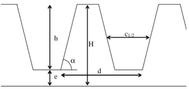
α h
e
c1/2
Multilayer dielectric stack H
d
Fig. 1. A silica layer of thickness H is coated on a dielectric mirror made of HfO2 and SiO2
layers reflecting more than 99.5 % of the incident light (λ=1053 nm and θ=72°). A grating is ion etched in the silica layer with a period d, a groove height h, and a groove width at the half depth c1/2. The residual thickness of the silica layer is denoted e. Pillars present a trapezoidal
geometry with angle of slope α.
We are interested in this section by the design of the grating profile as a function of the variables h, c1/2 and α. The goal is to reach a uniform efficiency on the surface of the grating
(420x450mm²) higher than 95 % in the (-1) order in reflection, and a very low enhancement of the electric field intensity inside the grating. The numerical treatment is made with the use of the differential method which resolves Maxwell equations in periodic media. The recent improvements of the method such as the S-matrix propagation algorithm and the fast Fourier factorization method are included in the code13. The electromagnetic field is developed onto a discrete and truncated Fourier basis, which permits the reduction of Maxwell equations onto a set of first order differential equations. A first integration of this set of equations from the substrate to the superstrate, with the knowledge of the incident field, leads to the calculation of the electromagnetic field in both substrate and superstrate media. A second integration permits the calculation of the electromagnetic field inside the modulated area. The discretization steps Δh=0.05h, Δc1/2=20 nm and Δα=1° are taken approximately equal to the
half of the manufacturing incertitude, i.e. the half of the variations of the variables over the surface of the grating, and the ranges are h=[0;H], c1/2=[300 nm; 420 nm] (d=562 nm) and
α=[82°;84°]. In a first step, reflected efficiencies in the (-1) order are calculated for the whole set of combinations {h, c1/2, α}. Then for each combination {h, c1/2, α}i , the mean and the
variance of the efficiency are calculated for the 27 nearby profiles: h+iΔh, c1/2+iΔc1/2,
α+iΔα with i={−1;0;1}. If the mean reflected efficiency is higher than 95%, then the electric field reconstruction inside the modulated area is undertaken and the maximum of the electric field enhancement in the silica is stored. The mean reflected efficiency has to be maximized
while the variance efficiency and the maximum of the electric field enhancement in silica have to be minimized. It has been shown in previous studies that the electric field is localized inside the grooves, and that thin pillars avoid a large penetration of the strong electric field inside pillars10-12.
3. Short pulse damage test setup
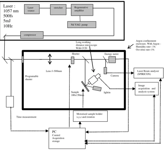
The experimental setup (Fig. 2) developed for laser damage testing uses a chirped-pulse-amplified laser system, developed in the laboratory. The source laser is a commercial diode pumped laser (TBW GLX200), producing a 10 nJ pulse at 100 MHz. The pulse duration is 200 fs at 1057 nm with 8 nm spectral bandwidth. The laser is stretched with a four-pass grating device (1740 l/mm groove density) and amplified through a Ti:Saphire regenerative amplifier. The pump laser is a frequency-doubled Nd:YAG laser Quantaray GCR150 (SPECTRA PHYSICS) operating at a repetition rate of 10 Hz. Before compression, the pulse duration is nearly 1 ns and the energy can reach 5 mJ. After compression with a four-pass gratings device, the duration is reduced down to 500 fs. Pulse duration is controlled with a single shot autocorrelator.
Laser : 1057 nm 500fs 5mJ 10Hz Camera Lens f=500mm Long working distance microscope With CCD
Motorised sample holder x,y,z and rotation
Laser Beam analyser (SPIRICON) Image acquisition and analysis system Sample 100x150mm lightin Energy meter PC Control Acquisition storage Programable shutter Time measurement Laser source stretcher Regenerative amplifier Nd YAGpump compressor Argon confinement enclosure. With Argon : Humidity rate< 1% Oxygène rate<1% Shutter
Fig. 2. Experimental setup for laser damage testing
For damage testing, the beam is focused with a 500 mm focal-length lens. The sample is set on a three axes motorized holder, at the lens focal plan. A rotation stage allows testing the sample at various angles of incidence, while keeping the front surface at the focal plane. The beam profile is nearly a gaussian profile with a diameter of 200 µm at 1/e² (Fig. 3).
Fig. 3. Spatial profile of the focused laser used for testing. Diameter of 200µ m at 1/e²
By using a half-wave plate before the compressor, the energy can be adjusted on the sample. The energy of each pulse is measured from a split-off portion of the beam by an energy meter (OPHIR PD10) first calibrated with an energy meter OPHIR PE10. The fluctuation of the energy is ± 5 % (deviation at 2σ). The beam profile is measured with a CCD (COHU 7713) placed in a plane equivalent to the sample optical plane. A beam-analyzer system LBA PC400 is used to record each spot. A programmable shutter inserted after the lens allows choosing the kind of test performed on the sample: 1 on 1 or S on 1 procedure.
During the test, the irradiated site of the sample is monitored with a long-working-distance microscope equipped with a CCD camera (resolution of about 10 µm). The bench is located in a confinement enclosure (glove box) to operate under dry air (RH<10%) or argon atmosphere (RH<1%). These conditions limit potential self focusing effects or plasma generation in air.
The density if energy is given by Eq. 1:
eq S
F= ξ , (1)
where ξ is the energy and Seq is the equivalent area for each pulse. The equivalent area Seq
is measured from the spatial profile given by the beam analyzer as the ratio of the entire energy by the maximum density of energy:
pixel i i i eq S Fi Fi n S × × =
∑
= = max max min ) ( , (2) where Spixel is the elementary area of a pixel, ni is the number of pixels of fluence Fi andFimax is the intensity maximum.
Fluences are given in beam normal and the fluctuation is ± 9% (deviation at 2σ). The threshold damage data are deduced from the probability of damage. A minimum of 200 sites are exposed to a burst of 100 laser pulses at a specified fluence. The damaged sites are observed with the microscope and the number is recorded. This operation is repeated for different fluences to express a damage probability as a function of fluence.
Self focusing is known to be an important parameter for the design of short pulse laser damage setups. Consequently, we numerically estimated the B-integral through the focal volume prior to the test surface. In our system B-integral is due to the self focusing in the air after the last focusing lens of focal f = 0.5 m. For a Gaussian beam with a wavelength λ and waist radius w1, let's define the Rayleigh distance ZR:
λ π 2 1 w ZR= ⋅ (3)
The intensity I at the focal spot is given by the relation: 2 1 . . 2 w I π τ ξ = (4)
Where ξ is the energy and τ the pulse duration. The B-integral can be estimated by:
∫
= R Z dz z I n B 0 2 ( ) 2 λ π (5)If we assume that the intensity I is constant within the Raleigh distance ZR, combination
of Eq. (3), (4) and (5) gives:
τ ξ λ π 2 2 4 n B= (6)
With our system, we have tested samples up to 8 J/cm² in the beam normal at 500 fs. This fluence is obtained with an energy of 0.9 mJ. For testing carried out in air, nonlinear refractive index14 is n2 = 3.10-19 cm²/W and Eq. (6) gives a B-integral value of B ~ 0.6. We are therefore
below but not so far from the self focusing limit which can be taken at B ~ 1. Let's outline that Jovanovic et al15 while evaluating the capabilities of a rather similar short pulse testing damage setup have shown that self focusing appears when the energy increased above 1.5 mJ for 200 fs pulses. We are well below this ξ/τ ratio in our experiment.
From an experimental point of view, we also checked that while increasing the fluence during the test of a sample well above the damage threshold up to 10 J/cm², the damage probability kept constant at 100%. We have not noticed any random probability at high fluences as it could be suspected in presence of non linear effects. Moreover, damage morphology stays elliptical with no pinpoints typical of self focusing.
An example of a 1740 l/mm gold coated grating tested at 72.5° in TM polarization is given on Fig. 4. It can be seen that the threshold measured is in good concordance with previous works7-9.
0,000 0,100 0,200 0,300 0,400 0,500 0,600 0,700 0,800 0,900 1,000 0,00 0,25 0,50 0,75 1,00 1,25 1,50 1,75 2,00 2,25 Fluence (J/cm²) P ro b a b il it y
Fig. 4. Example of damage probability on a 1740 l/mm gold grating. Testing is done at an incidence of 72.5° in TM polarization. The damage threshold i.e. maximal value at which damage probability is null is 0.67 J/cm²
Finally, we damage tested a 1740 l/mm grating manufactured in 2005 at Horiba Jobin Yvon on a MLD mirror coated by the Laboratory for Laser Energetics (LLE) of the University of Rochester. This grating had been damage tested at LLE in april 2005 and was cross tested on the DERIC setup. The damage threshold measured on DERIC is 2.1 J/cm² in normal beam while being tested at an incidence of 72.5° and 500 fs while the damage threshold measured at LLE was 4.487 +/- 0.089 J/cm² at an incidence of 61° for 10 ps pulses in N/1 mode. This threshold is equivalent to ~2.7 J/cm² at an incidence of 72.5° for 500 fs pulses using an angular projection and a 0.33 temporal scaling law16. The damage threshold measured on DERIC setup is close from the result obtained by LLE. The relatively small difference can be due to the temporal scaling law and angular projection approximations, the differences of the damage setup (focal spot size, number of shots per site…) and the part possible aging since tests were carried out in two years time.
4. Design and manufacturing of MLD grating
Optimization of a MLD grating begins with the design of the dielectric mirror stack. The MLD mirror stack is a modified quarter wave HfO2/SiO2 (HL)7H mirror manufactured by
SAGEM17 on Pyrex substrates with an additional low index top layer dedicated to the grating modulation. The stack is engineered to cope with various specifications18, 19. Both transmitted orders of the grating must be reflected. For our line density of 1780 l/mm, the mirror must have a reflectivity of more than 99.5% at 1.053 µm for an incidence of 70.6° under vacuum. The mirror shall keep its integrity while being processed during the grating etching and the MLD grating operation under vacuum. It shall typically not craze.
Once the mirror stack is retained, the grating pattern is optimized thanks to the numerical method presented in section 2. Four 120 x 140 mm² 1780 l/mm MLD gratings were manufactured by Horiba Jobin Yvon. The samples were then controlled in terms of diffraction efficiency, groove profile and damage threshold. Groove profile is measured with an Atomic Force Microscope (AFM) on various position of each sample. Figure 5 shows an example of such a measurement on PW08 sample. Finite width of the AFM tip induces incertitude on the profile measurement. Measurements on calibrated references have shown that incertitude on h is +/-3% and on groove width over period ratio (c1/2/d ratio) is +/-0.03.
Fig. 5. AFM measurement on PW08 sample – section analysis
Diffraction efficiency is measured at 77.2° incidence and wavelength of 1053 nm in TE polarization on a dedicated scanning photometer on the whole clear aperture of the part with a 2 mm x 4 mm sampling step. Figure 6 is an example of such a measurement on the PW08 sample.
Fig. 6. -1R diffraction efficiency in % measured on PW08 sample, coordinates in millimeters
Diffraction efficiency is very uniform. Table 1 present the characteristic of the different MLD gratings obtained. We took care to evaluate the diffraction efficiency on an area close to the one used for the AFM measurement; this measurement is confirmed by a calculation using the AFM profile data. Sample PW02 is a mirror without grating engraved on top; the mirror is the same as those of the other MLD samples.
Table 1. MLD gratings manufactured. Sample PW02 is a mirror without a grating
Serial number e (nm) h (nm) c1/2 (nm) -1R diffraction efficiency, TE,77.2° E² maximum calculated in the MLD, TE, 77.2° PW01 0 303 264 95% 2.34 PW04 75 386 433 96% 1.43 PW08 18 440 365 95.8% 1.40 PW10 64 396 382 96.2% 1.69 PW02 458 0 0 - 0.20
It can be seen that the E² value in the MLD is distributed from 2.34 to 1.4. The E² and data are calculated with the groove pattern obtained from the AFM measurements.
(a)
(b)
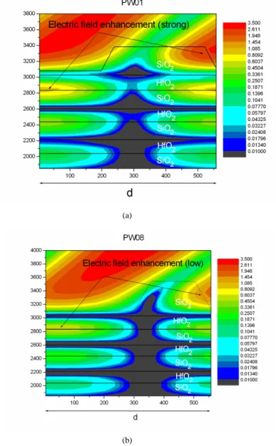
Fig. 7. Reconstruction of E² in the top area of gratings PW01 (a) and PW08 (b)
Figures 7(a) and 7(b) respectively show the reconstruction of the normalized electric field intensity E2 in the top area of the samples PW01 and PW08. The small values of h and c1/2 of
sample PW01 compared to sample PW08 explain the strong enhancement of the electric field inside the pillars made of silica in grating PW01.
We also tested parts PW01 and PW04 at 64.05°, the angle paired with 77.2° through grating diffraction. At this incident angle, the electric field enhancement is increased while the diffraction efficiency remained the same as shown in table 2.
Table 2: Electric field intensity enhancement Serial number e (nm) h (nm) c1/2 (nm) -1R diffraction efficiency, TE, 64.05°
E² maximum calculated in the MLD, TE, 64.05°
PW01 0 303 264 95% 4.46
PW04 75 386 433 96% 3.09
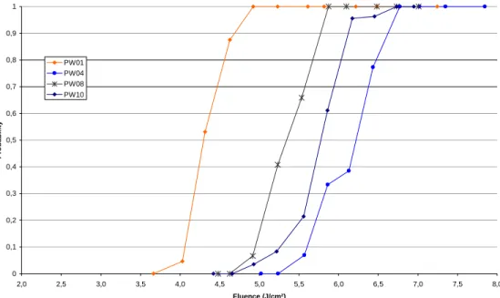
5. Results
The four samples detailed above were tested on the DERIC facility described in section 3. Testing is carried out under 10% RH air environment at an incidence of 77.2° in TE polarization. Damage probability is evaluated on the zone used for AFM and efficiency measurement in order to be sure to associate a given threshold with a E² value corresponding to the real groove pattern. Thresholds are expressed in beam normal. Obtained results are presented on Fig. 8. 0 0,1 0,2 0,3 0,4 0,5 0,6 0,7 0,8 0,9 1 2,0 2,5 3,0 3,5 4,0 4,5 5,0 5,5 6,0 6,5 7,0 7,5 8,0 Fluence (J/cm²) P ro b a b il it y PW01 PW04 PW08 PW10
Fig. 8. Damage performance at 1.053 µm, 77.2°, TE polarization, 500 fs of 4 MLD samples
Damage testing procedure was repeated on different zones on each part. Figure 9 shows the variation of the damage threshold on the surface of sample PW01. The damage threshold is defined with the norm NF EN ISO 11254-1 as the last null point of the statistic.
0 0,1 0,2 0,3 0,4 0,5 0,6 0,7 0,8 0,9 1 2,0 2,5 3,0 3,5 4,0 4,5 5,0 5,5 6,0 6,5 7,0 7,5 8,0 fluence (J/cm²) P roba bi lit y PW01 Zone 1 95% PW01 Zone 2 94,2% PW01 Zone 3 97,6%
Fig. 9. Damage performance at 1.053 µ m, 77.2°, TE polarization, 500 fs on different zone of PW01 sample with corresponding measured diffraction efficiency
Damage threshold stays quite constant. We notice that the better threshold corresponds to the highest diffraction efficiency where the profile presents the best concordance to the calculated design. This behaviour is similar on the other samples.
6. Discussion
Figure 10 gives the dependence of damage threshold with the electric field enhancement calculated using AFM measurement (see section 4) and DERIC damage testing (see section 3) of the manufactured samples.
R2 = 0,965 0 1 2 3 4 5 6 7 8 9 0 1 2 3 4 5 1 / F. E D a m a g e th re s h o ld in b e a m n o rma l (J /c m²) PW01 @ 77.2° PW04 @ 77.2° PW10 @ 77.2° PW08 @ 77.2° PW02 Mirror @ 77.2° PW01 @ 64,05 PW04 @ 64,05
Fig. 10. Damage performance at 1.053 µ m, 77.2° or 64.05° of incidence, TE polarization, 500 fs versus 1/ E² maximum on four different MLD samples and a mirror (PW02).
The ratio of the damage threshold (DT) value of two gratings (g1 and g2) is equal to the inverted ratio of their field enhancement (F.E):
DT (g1) / DT(g2) = F.E. (g2) / F.E. (g1) (3) As a consequence, the points are found on a linear fit with a correlation factor of 0.96. With a given grating profile, the damage threshold can be predicted by calculating the maximum electric field enhancement in the grating material.
It can be noticed for PW08 that while exhibiting a slightly lower field enhancement than PW04, PW08 exhibits a rather lower damage threshold. We believe that this can be attributed to the incertitudes of both the damage threshold and AFM profile measurements.
The mirror damage threshold point stands apart from this law. We see two possible explanations for this. First, as detailed in section 3, the B-integral becomes close to unity when fluence increase up to 8 J/cm². Measured damage threshold can therefore be erroneous. Second, the position of the electric field maximum in the mirror is different from the grating. In a MLD grating this maximum is located about 100 nm below the top layer along a pillar while in a mirror it is located in the middle of the top low index layer. The SiO2 low index
material is probably not in the same state in these two cases. Moreover, grating manufacturing process shall also modify the SiO2 layer. Consequently, it is difficult to conclude on the mirror
sample.
Regarding damage thresholds values, they are in the range of 3.5 J/cm² to more than 5 J/cm² in normal beam at an incident angle of 77.2°. These values are quite a bit higher than previously published data on MLD gratings. Barty20 reports a damage threshold of 2.5 J/cm² at 1 ps on a 1780 l/mm MLD grating at 77.2°. It is equivalent to ~2 J/cm² at 500fs using a 0.33 temporal scaling law16. Keck21 reports a damage threshold of 5.16 J/cm² on 1740 l/mm MLD gratings at 10 ps. It is equivalent to ~2.6 J/cm² at 500fs for a 1780 l/mm part at 77.2° using the same temporal scaling law and an angle projection. If our thresholds are beyond the experience of other laboratories, they are still below the damage threshold of fused silica measured at 2 to 2.5 J/cm² at 500 fs and normal incidence8. They are also below the threshold of a SiO2 monolayer deposited by Ion Beam Sputtering (IBS) measured by Mero16 at 5 J/cm² for a 500 fs pulse duration, normal incidence and a wavelength of 0.8 µm.
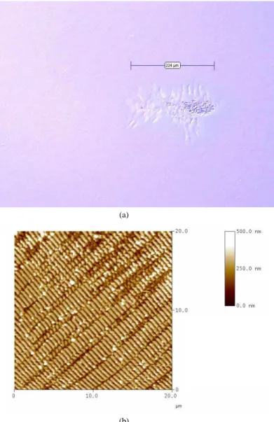
We have also studied the damage morphology. Large field observation is made on a REICHERT Nomarski microscope. More precise observations are made on an AFM. Damage morphology is very similar on samples PW01 and 08. We noticed a periodic pattern perpendicular to the grating line. The pattern seems to exist prior to the total ablation and was previously reported by Kosc22. The period of the ripples is approximately 2 µm.
(a)
(b)
Fig. 11. Damage on sample PW01. (a) A periodic pattern perpendicular to the gratings lines is lightly visible on the periphery of the damage. (b) an AFM observation of the periodic ripple.
On sample PW04, this specific behaviour is less present, and the pattern could be seen only on two damage sites. Damage morphology is quite different from the previous samples with more completely ablated damages as depicted on Fig. 12.
Fig. 12. Damage on sample PW04. No ripples are observed.
We could not find any correlation between MLD grating profile and the existence of this specific pattern.
We also tried to have a look at damage of the grating grooves. For this purpose, AFM measurements were made on damage sites of different samples. We could not see the specific damage morphology noticed by Stuart9 with damage initiating on the edge of the groove opposite to the incident light where the electric field is maximal. The S on 1 damage testing procedure retained in our experiments might be responsible for that. With about 200 shots per sites, damage growing is the prevalent phenomenon resetting the signature of damage initiation. Despite this, some evidence of the role of the electric field can be seen on the damage morphology. Figure 13 shows a section analysis made on a damage of sample PW04. We notice that the grooves are destroyed and that the damage depth (approx. 700 nm) corresponds to the second E field maximum at the second SiO2/HfO2 interface (see Fig. 7).
Fig. 13. AFM scan on a damage on PW04 sample. Top: section analysis. Bottom left: 2D view. Bottom right: spectrum
7. Conclusion
Damage testing at 500 fs, 1.053 µm wavelength was carried out on various 1780 l/mm MLD gratings and mirror samples. Testing was done at a fixed angle of incidence around the Littrow angle. Each sample was manufactured to exhibit a different electric field enhancement inside the MLD stack. This enhancement was calculated using a numerical treatment using the differential method to solve Maxwell equations in periodic media. Close optical and AFM inspection of damage sites shows that damage occurs where the electric field is maximum. Periodic ripples observed by Kosc22 were also noticed but not related to a specific grating and testing geometry. Experiments and electric field calculation evidenced that, for a given line density, and given materials, damage threshold of MLD grating at 500 fs is governed by the value of E².
Acknowledgments
This work was supported in part by the Conseil Régional d’Aquitaine and is performed under the auspices of the Institut Lasers et Plasmas. DERIC damage testing facility development was performed under the auspices of Laserlab European program. We thank the ALISÉ team for access to and modular capabilities of ALISÉ facility. We thank the Laboratory for Laser Energetics of the University of Rochester for providing a 1740 l/mm MLD grating with its measured damage threshold for cross testing purposes. We thank C. Rouyer and H. Bercegol for helpful discussions and corrections of our work.