Development of an Architectural Design Tool
for 3-D VLSI Sensors
by
Brian Tyrrell
B.S.E., University of Pennsylvania (1998)
Submitted to the Department of Electrical Engineering and Computer Science in partial fulfillment of the requirements for the degree of
Master of Science in Electrical Engineering at the
MASSACHUSETTS INSTITUTE OF TECHNOLOGY
Author
June 2004
©
Massachusetts Institute of Technology 2004. All rights reserved... ... ...
Department oi rAec1ricai Iiiiimimri-, -. mputer Science
May 7, 2004 C ertified by ...
Associate Department Head and Professor
Certified by... Assistant Leader L. afael Reif of Electrical Engineering -sis Supervisor .... ... 1 ... Robert K. Reich achnology Group 'ksiSupervisor Accepted by ... ... Arthur C. Smith ulnairman, Department Committee on Graduate Students
This work was sponsored by the United States Air Force under Contract F19628-00-C-0002. Opinions, interpretations, conclusions, and recommendations are those of the author and are not necessarily endorsed by the United States Government.
MASSACHUSETTS INSMMTUT
OF TECHNOLOGY
APR
0
4
2006
BARKER
Development of an Architectural Design Tool
for 3-D VLSI Sensors
by
Brian Tyrrell
Submitted to the Department of Electrical Engineering and Computer Science on May 7, 2004, in partial fulfillment of the
requirements for the degree of Master of Science in Electrical Engineering
Abstract
Three dimensional integration schemes for VLSI have the potential for enabling the development of new high-performance architectures for applications such as focal plane sensors. Due to the high costs involved in 3-D VLSI fabrication and the fabri-cation complexity of 3-D integration, analysis of the design and process tradeoffs for a particular application is essential. An architectural and topological design tool is presented that enables the high-level analysis and optimization of sensor architectures targeted to a variety of 3-D VLSI process options. This design tool is based on an inference chain evaluation framework, and allows for a high-level structural represen-tation of a circuit architecture to be considered in conjunction with low-level process models. Approximation strategies for projecting circuit area and performance are incorporated into the inference chain relations.
Thesis Supervisor: L. Rafael Reif
Title: Associate Department Head and Professor of Electrical Engineering
Thesis Supervisor: Robert K. Reich
Title: Assistant Leader of the Lincoln Laboratory Advanced Imaging Technology Group
Acknowledgments
First, I would like to thank the Lincoln Scholars Program (LSP) Committee at MIT Lincoln Laboratory for its support of this work. I am especially indebted to Dr. Robert O'Donnell, who encouraged me to pursue graduate study through the LSP. A special thanks also goes out to my advisors, Prof. Rafael Reif of the MIT Electrical Engineering and Computer
Science Department and Dr. Robert Reich of Lincoln Laboratory.
I also owe a debt of gratitude to many Lincoln staff members in the Advanced Sili-con Technology and Advanced Imaging groups who provided much needed assistance and feedback throughout the research process. A particular thanks goes out to Dr. Robert Berger, Dr. Charles Stevenson, Dr. Brian Aull, Dr. David Shaver, Bruce Wheeler, Antonio Soares and Keith Warner. Just as important are those who provided critical administrative support, especially Susan Moriarty. The library staff at Lincoln Laboratory also provided a tremendous resource and helped shave off valuable hours by streamlining the research process.
Finally, without the support of my family, academic work would have been impossible.
My wife, Lanaanne, and sons Jacob, Jonathan and Jeremiah have put up with my long hours
and crankiness for quite some time. I am also grateful for the useful feedback Lanaanne provided concerning both the content and the presentation of this thesis work.
... as we know, there are known knowns; there are things we know we know. We also know there are known unknowns; that is to say we know there are some things we do not know. But there are also unknown unknowns - the ones we don't know we don't know. And if one looks throughout the history of our country and other free countries, it is the latter category that tend to be the difficult ones.
-Donald Rumsfeld 12 February 2002
Contents
1 Introduction 15
1.1 M otivation . . . . 15
1.2 Concise Background . . . . 16
1.3 Objective of This Thesis Work . . . . 19
1.4 Technical Approach . . . . 21 1.5 Nom enclature . . . . 23 1.5.1 Term inology . . . . 23 1.5.2 Typographical Conventions . . . . 25 2 Essential Background 27 2.1 3-D Fabrication Technologies . . . . 27
2.2 Image Sensor Architectures . . . . 28
2.2.1 Focal Plane Array Design Constraints . . . . 28
2.2.2 Analog-to-Digital Converter Technologies . . . . 30
2.3 Foundational EDA Infrastructure . . . . 31
2.3.1 The GTX Framework . . . . 32
2.3.2 Verilog-AMS Capabilities . . . . 34
3 GTX Model Development for 3-D VLSI Processes 37 3.1 New GTX Literals and Parameters . . . . 37
3.2.1 Process Flow Representation . . . . 39
3.2.2 Inter-tier Via Interactions . . . . 42
3.2.3 Quantitative Process Parameters . . . . 42
3.2.4 Error Propagation and Production Volume . . . . 43
3.2.5 Alignment Methods . . . . 53
3.2.6 Calculation of Inter-tier Via Design Rules . . . . 55
3.2.7 Design Grid . . . . 57
3.2.8 Determination of Exclusion Regions . . . . 57
3.2.9 Case Study: Active-Dominated vs. Interconnect-Dominated C ircuits . . . . 61
3.3 Sum m ary . . . . 63
4 Interconnect Modeling for Conceptual Design 65 4.1 Level Representation . . . . 66
4.1.1 Ordering of Levels . . . . 66
4.1.2 Definition of Level Usages . . . . 66
4.1.3 Example of Interconnect Skeleton: Snapshot Mode Imager with Very Short Integration Time . . . . 68
4.2 Representation of Grid-Type Interconnect . . . . 68
4.3 Supply Rail Droop Modeling . . . . 71
4.3.1 Nodal Analysis of 1-D Supply Rail . . . . 73
4.3.2 Nodal Analysis of 2-D Supply Rail . . . . 74
4.3.3 Voltage Divider Superposition Analysis of 1-D Supply Rail . 75 4.3.4 Voltage Divider Superposition Analysis of 2-D Supply Rail . 76 4.3.5 Input Parameters for Droop Voltage Modeling . . . . 81
4.3.6 Droop Voltage Evaluation Using Direct Nodal Analysis . . . . 82
4.3.7 Droop Voltage Evaluation Using Voltage Divider Superposition A nalysis . . . . 84
4.4.1 M iller M ultipliers ... . 91
4.4.2 Evaluation of Parasitic Capacitances . . . . 91
4.4.3 Case Study: Slew-limited Line Driver . . . . 96
5 Module Placement Optimization Using Simulated Annealing 99 5.1 Optimization Heuristic . . . . 99
5.2 Case Study: Application of Simulated Annealing to a LADAR Imager 101 5.2.1 LADAR Modules . . . 103
5.2.2 Floorplan Construction Using Actual Design Parameters . . . 103
5.2.3 Effect of Number of Tiers . . . . 106
5.2.4 Sum m ary . . . . 107
6 Verilog-AMS and SPICE Interface 109 6.1 Template Files: Verilog-AMS Output Example . . . . 109
6.2 Template Files: SPICE Deck Output Example . . . 112
7 Conclusion 115 7.1 Sum m ary . . . . 115
7.2 Future W ork . . . . 117
7.2.1 Interface Improvements . . . . 117
7.2.2 Enhancements to Process Models . . . . 117
7.2.3 Enhancements to Circuit Performance Projection Models . . . 118
7.2.4 Generalization of Simulated Annealing Cost Function . . . . . 118
7.2.5 Improvement of Computational Efficiency . . . . 119
A Discovered GTX Flaws and Limitations 121
B GTX Disclaimer 123
D Known Limitations To 3-D Process Models for GTX and Suggestions
for Future Development 129
E Summary of Parasitic Capacitance Model Equations 131
E .1 N otation . . . . 132
E.2 Survey of Empirical Models ... ... 132
E.3 Models Presented in 1998 by Wong et al. [54] ... 134
E.4 Nearbody capacitors with no ground plane . . . . 137
F 3-D Fabrication Technologies 139 F.1 The MITLL Post-bond 3-D Via Process . . . . 139
F.2 The MIT MTL Pre-bond 3-D Via Process . . . . 146
List of Figures
1-1 Typical signal flow path for an imager system . . . . 18
1-2 Power consumption for a typical signal path . . . . 19
1-3 EDA flow for conceptual design of 3-D sensors . . . . 22
2-1 Two 3-D integration methods . . . . 28
2-2 Structure of the GTX framework [11] . . . . 33
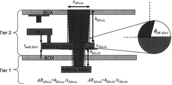
3-1 Illustration of dimensional parameters for pre-bond inter-tier via im-plem entation . . . . 47
3-2 Illustration of dimensional parameters for post-bond inter-tier via im-plem entation . . . . 47
3-3 Example of alignment tree . . . . 54
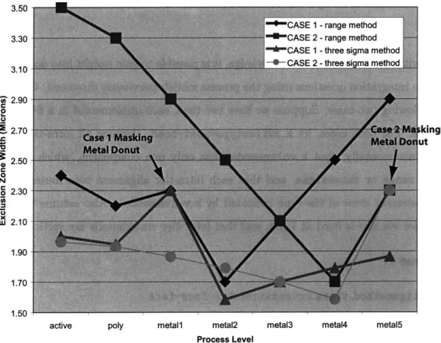
3-4 Example exclusion zone study . . . . 62
4-1 Example of interconnect skeleton: snapshot-mode imager with short integration tim e . . . . 69
4-2 Resistor line segments for 1-D supply grid modeling . . . . 73
4-3 Resistor grid for 2-D supply grid modeling . . . . 74
4-4 32 x 32 array with one 0.1 mA source at (4,4) . . . . 86
4-5 32 x 32 array with one 0.1 mA source at (12,12) . . . . 87
4-6 32 x 32 array with one 0.1 mA source at (7,7) and various resistor ratios 88 4-7 Droop peak for various resistor ratios . . . . 89
4-9 Scaling of droop calculations to large arrays . . . . 4-10 Simulated nearbody capacitance and capacitance to substrate for
var-ious ILD thicknesses . . . . 4-11 Some parasitic capacitances in a 3-D circuit . . . . 4-12 Interconnects in an example pixel . . . . 4-13 Required line driver current vs. pixel size . . . .
5-1 Concept (a) and 3-D implementation (b) of LADAR imager [6, 7] . . 5-2 LADAR imager pixel size vs. number of tiers for three different sets of design rules . . . .
C-1 Two intersecting circles of arbitrary size and spacing . . . . E-1 Parasitic capacitance components . . . . E-2 Primitive capacitance structures [54] . . . . F-1 Individually processed SOI and bulk wafers .
F-2 First wafer bonding step . . . . F-3 First set of 3-D vias . . . . F-4 Second wafer bonding step . . . . F-5 Second set of 3-D vias . . . . F-6 3-D imager configured for backside imaging. F-7 3-D via layout examples . . . . F-8 Initial set of processed SOI wafers . . . . F-9 Definition of inter-tier vias . . . . F-10 Formation of Cu bond pads . . . . F-11 Two-tiered structure after Cu-Cu bonding .
90 94 96 97 98 102 106 12b 133 135 140 141 141 142 142 143 145 147 147 . . . . . 148 . . . . . 148
List of Tables
3.1 Process flow description parameters . . . . 40
3.2 Process parameters relating to alignment . . . . 44
3.3 Process parameters relating to default widths and spacings for certain classes of levels . . . . 45
3.4 Process parameters representing feature widths, spacings, and thicknesses 46 3.5 Additional process parameters relating to physical measurements . . . 48
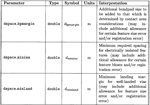
3.6 margin parameters . . . . 49
3.7 Calculated exclusion region parameters. . . . . 58
3.8 GTX rules for modeling 3-D processes . . . . 64
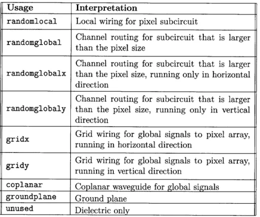
4.1 Level usages in k-usage-levelsTX . . . . 67
4.2 Signal param eters . . . . 70
4.3 Topological parameters . . . . 72
4.4 Capacitances of wires over gratings and groundplanes . . . . 95
5.1 Modules in the LADAR pixel . . . 104
5.2 Simulated annealing results for actual LADAR design conditions . . . 105
F.1 Version 5.11 (Jan. 2002) and *version 6.mosaic (July 2003) MITLL 3-D process design rules . . . 144
Chapter 1
Introduction
1.1
Motivation
Over the past several decades, transistor technology development has focused on reduction of process critical dimensions (CD) and supply voltages. This has been primarily driven by high-volume digital applications. For many analog applications requiring a large dynamic range, further scaling beyond the 0.25 Pm-node has yielded diminishing benefits. Now, as device-to-device interconnect limitations begin to dom-inate in digital VLSI systems, new technologies are emerging that may also prove beneficial for many analog and mixed signal applications. One especially promising new technology is three-dimensional (3-D) integration.
Three-dimensional integration schemes for VLSI have the potential for enabling the development of new high-performance sensor architectures for applications such as focal planes, chemical and biological agent detectors and micronodes. In particular, 3-D VLSI technology is well suited to problems that can benefit from the use of parallel signal detection and processing paths, as well as those for which various stages of the signal path are best implemented in different technologies.
Because of the high costs involved in 3-D VLSI fabrication and the modular na-ture of 3-D integration, analysis of the design and process tradeoffs for a particular
application is essential. An architectural and topological design tool is developed to enable the high-level analysis and optimization of sensor architectures targeted to a particular set of 3-D VLSI process options. The ultimate goal of this research is the development of a tool that can be used in the conceptual phases of a design to analyze the tradeoffs inherent in the available architectural and process options. This information is particularly useful in cost-benefit analyses of proposed systems, and in selection of appropriate wafer processes for each tier of a potential 3-D integrated die. The ultimate goal is to facilitate the determination of the most promising approach for a particular application.
By its very nature, electronic design automation (EDA) for 3-D mixed signal circuits is an important but technically difficult problem. This work will provide the groundwork for a 3-D EDA tool. Further enhancements by future investigators are to be expected.
1.2
Concise Background
Over the past several years, increasing attention has been directed toward the three-dimensional integration of VLSI circuits. This development has primarily been driven by the demands of digital applications, but tangible benefits are projected for analog applications as well. It has been demonstrated that the three-dimensional stacking of multiple active device layers can significantly reduce the number of long global and semi-global interconnects. [35, 36] Since digital VLSI systems are increasingly limited by the performance of the back end, significant speed and power benefits are anticipated.
There are a number of 3-D integration schemes presently under development. One approach uses low temperature silicon epitaxy to achieve vertical integration. [12] Although there exists the potential for high vertical connectivity with this method, thermal budget considerations would likely limit such processes to a small number of
active device layers. An alternative method uses low temperature wafer bonding of processed wafers to form a multi-tiered structure.[9, 37] Since each tier of the final die corresponds to an individually processed wafer, a tremendous degree of process flexibility is possible with this method. For example, multiple material systems may be used, thermal budgets for each tier are essentially independent, and the number of active device tiers is limited primarily by the yield and reliability of the bonding process and other mechanical and thermal constraints. The particular 3-D processes considered in this study are discussed in further detail in chapter 2.
Wafer-bonded 3-D processes may offer considerable benefits for analog and mixed signal designs. 3-D stacking of state-of-the-art digital CMOS devices on top of analog-optimized wafers with larger gate CD has been getting increasing attention.[25] One possible early application of wafer-bonded processes is in the area of solid state im-agers. This is an area of considerable ongoing research. [9, 24, 28, 29] The EDA design aid presented here finds its intended application in this area of integrated imagers.
The EDA infrastructure necessary for enabling design of commercial 3-D inte-grated circuits is not yet in place for digital applications. There has been exten-sive research pertaining to the modeling of interconnects in such systems.[16, 35, 36] Based on these interconnect models, some digital place and route algorithms have been implemented. [33, 34] For full-custom design, a 3-D extension of the MAGIC CAD tool has been developed. [4] However, very few EDA design aids exist for analog and mixed signal design, even for conventional 2-D integration.
The conceptual stages of 3-D imager design are well suited to automation. Any proposed imager architecture can be described as a set of signal processing paths, each composed of well-understood sub-blocks. For most 2-D imager designs, the topology of the imager is easily anticipated, thus eliminating the need for semi-automated pre-design. In this conventional case, the size of the pixel places a strict limit on the complexity of the per-pixel circuitry, thus limiting the design options. With the introduction of 3-D integration technology, the set of achievable architectures
increases tremendously since more of the signal processing can be implemented within the pixel itself. This leads to a new set of design tradeoffs, not the least of which is that between the parallelism of the signal processing and the number of tiers of active devices.
The purpose of the described tool is to facilitate the exploration of these new tradeoffs in the initial stages of architectural design. It will allow circuit architectures to be defined at a high level so that their performance may be evaluated prior to the more expensive phases of the design cycle. It will also aid in the determination of an initial floor plan that makes good use of the process flexibility that wafer bonding technology offers the circuit designer.
For most imaging systems, the signal processing path is generally described as follows.[27] As illustrated in the signal flow diagram of figure 1-1, the incident radia-tion, here indicated as "light," generates an analog response in the detector. This is typically subject to analog conditioning prior to analog to digital conversion (ADC) and subsequent digital processing. In some applications, particular components of this signal flow are eliminated. For example, in Geiger mode avalanche photodiode based photon counting and LADAR imagers, the photodetector is designed to pro-duce a full digital swing, which can then serve as a direct input to digital signal processing. [6]
Detector Analog A/D Digital
Processing Conversion Processing
Figure 1-1: Typical signal flow path for an imager system
The detector and the input to the analog processing are always implemented in a per-pixel manner. The remainder of the analog processing stage, the ADC and the digital processing may be implemented in a per-pixel manner, shared by a set of pixels, or implemented once for the array. In addition, the functions of each of these blocks may be broken up into a per-pixel component or a shared component.
Increased functionality within the pixel can provide the benefits of improved signal to noise ratio, increased speed, and reduced power. The primary constraint limiting the addition of new functionality to the pixel is the maximum pixel area. 3-D integration can increase the available area for per-pixel processing, but this capability comes at the expense of an increased process cost and decreased yield.
A simplified illustration suggesting some of the tradeoffs inherent in the design of an imager is shown in figure 1-2.[27] Expressions for estimated power consumption of the analog processing, ADC, and digital processing are given. Note that the opti-mization of this system requires an understanding of the coefficients KA, KADC, and KD, which are technology and implementation dependent. Such an optimization is necessary in determining what aspects of signal processing are best managed at the analog front end or the digital back end.
Signal Analog - ADC N Digital
Input Processing Processing
Power = KA * BW -VDR2 Power = KADC -BW -VDR Power = KD -BW - log(VDR) VDR = voltage dynamic range BW = bandwidth
Figure 1-2: Power consumption for a typical signal path
In a 3-D design, new possibilities are introduced that affect this tradeoff. In particular, the analog processing may be made much more sophisticated and the ADC may be implemented at the pixel. It is even possible to place digital processing immediately behind the pixel array, allowing for massively parallel inputs.
1.3
Objective of This Thesis Work
Due to the high costs involved in 3-D VLSI fabrication and the modular nature of 3-D integration, analysis of the design and process tradeoffs for a particular
appli-cation is essential. This work investigates the incorporation of technology analysis into the front end architectural and topological design toolset to enable the high-level analysis and optimization of sensor architectures targeted to a particular set of 3-D VLSI process options. By combining Verilog-AMS behavioral modeling [1] with in-ference chain based technology extrapolation [11], automated analysis of technology constraints within the context of the circuit design process is implemented.
The intended inputs to this EDA flow are based on the combination of a param-eterized Verilog-AMS behavioral model and a set of associated GTX parameters and rules. (The GTX technology extrapolation framework is described in section 2.3.1.) Process data is likewise specified in terms of additional GTX parameters and rules. In a practical setting, a process library may be envisioned that contains a set of available process options, thus allowing for the exploration of optimal process technologies for each wafer tier. Sub-block models are constructed to be parameterized according to the available process technology space. The library of sub-block models may consist of a combination of existing precharacterized reusable intellectual property (IP) and generalized topological models that use empirical performance metrics to estimate the achievable performance of a proposed subsystem. Likewise, it is also feasible to allow for certain sub-block selection operations to be performed using an inference chain method similar to that used for deriving the behavioral parameters.
The intended output files consist of Verilog-AMS cases that are suitable inputs to conventional simulation engines, along with a set of inference chain derived metrics that provide the designer with an initial insight into the system performance even prior to behavioral modeling. After a number of iterations, a proposed system-level floor plan may be derived that suggests the optimum technology for each tier of the 3-D wafer stack, the optimum placement of subblocks within the stack, projected performance and other meaningful information.
The ultimate goal of this work is the development of a tool that can be used in the conceptual phases of a design to analyze the tradeoffs inherent in the available
architectural and process options. This tool may then be used in determination of the most promising approach for a particular application. This information is particularly useful in cost-benefit analyses of proposed systems, and in selection of appropriate wafer processes and circuit architecture for each tier of a potential 3-D integrated die.
1.4
Technical Approach
This work focuses on the development of an EDA solution that combines behavioral modeling with technology extrapolation to facilitate the tradeoff analysis required for architectural design of 3-D imagers. An attempt will be made to build upon much of the existing analog/mixed signal hardware description language (HDL) infrastructure. For that reason, a generalized output interface has been implemented that allows for projected circuit parameters to be used in conjuction with HDL representations in languages such as Verilog-AMS [1]. The technology extrapolation infrastructure of GTX, the MARCO GSRC Technology Extrapolation System [11] is used for inference chain evaluation. GTX is described further in section 2.3.1.
The EDA flow that has been implemented is illustrated in figure 1-3. The requisite "general knowledge" concerning 3-D integration, interconnect schemes, optimization algorithms etc. is represented in the form of GTX parameters and rules. Additional library data provides specific parameters and rules for a particular set of processes and circuits. By supplying process selections, design options, constraints, and application-specific models, a designer may initiate the inference chain implemented as part of the general knowledge, thus evaluating relevant descriptive parameters pertaining to predicted system performance. Some of these parameters may be used by an HDL model builder or SPICE model builder to allow for behavioral modeling. The designer then closes the feedback loop of the design flow by altering inputs based on knowledge gained.
DESIGNER
USER INPUT
-Process selections
-Possible design decisions
-Design constraints
-Circuit-specific models
GENERAL KNOWLEDGE
-Models for types of processes
-Models for types of interconnects
-Models for fundamental circuits
-Optimization algorithms
LIBRARY DATA
-Process Parameters *Library circuit knowledge
Figure 1-3: EDA
I
HDL INTERFACE -HDL model builder ecrinputs Pre-packagedThe foci of this work are the
"General Knowledge" and "HDL
Interface" blocks.
flow for conceptual design of 3-D sensors
interface" blocks of the design flow. Particular emphasis is given to the formulation of approximation startegies that allow for rapid projection of circuit performance parameters for various process and implementation configurations. Throughout this work, elements of the design flow are evaluated in two ways. First, assumptions and approximations are validated using accepted modeling techniques. In particular, Synopsys HSPICE and Silvaco Exact2 have been respectively selected as a circuit level simulator and a field solver. The utility of the developed EDA flow is demonstrated through its application to actual design situations. Thus, case studies are included that focus on particular aspects of the proposed flow.
1.5
Nomenclature
1.5.1
Terminology
Since 3-D VLSI technology is still in the early stages of development, much of the applicable terminology is not well established. The following definitions are used throughout this thesis work. In general, the terminology will follow that used in the design guide for the MIT Lincoln Laboratory 3-D FDSOI process.[2]
3-D via See inter-tier via.
design layer device plane inter-tier via interconnect plane level masking metal mating metal
A set of polygons in a layout database represent-ing a common design purpose. For example, the design layer METAL1 may define features on the first metal level of a VLSI process.
A plane of circuit features on levels correspond-ing to active area, implants, polysilicon gates, etc. which form active devices.
A via that connects interconnect planes on two tiers.
A plane of circuit features on metal and via levels.
A fabricated set of features formed in a particular lithography step.
In a post-bond 3-D via process, a metal layer that serves as both a hard mask in 3-D via formation and as an electrical contact. See section F.1.
In a post-bond 3-D via process, the metal layer onto which a 3-D via lands. See section F. 1. In a
pre-bond via process, the metal layer onto which each via from a Cu bond pad lands. See section F.2.
pre-bond 3-D via process A 3-D integration process in which part of the inter-tier via is formed on each of the wafers prior to bonding. The two surfaces are subsequently mated, forming the interconnected tiers. See section F.2.
post-bond 3-D via process A 3-D integration process in which inter-tier vias are etched after the wafers corresponding to the connected tiers have been bonded. See section F.1.
stratum See tier.
tier A combination of a device plane and one or more
proximate interconnect planes. A three-dimensional circuit is formed through the stacking of multiple tiers. In some sources, the term stratum is used in a synonomous manner.
In cases where the level of an intra-tier or inter-tier via must be referenced using a single number, it will be referenced using the level on which it lands, i.e. the lowest of the two level numbers. For example, a via connecting the first and second metal levels may be described as "vial." Likewise an inter-tier via connecting tiers two and three may be described as "3Dvia2." This convention will be useful in cases where index numbers must be used to refer to via levels. A similar situation arises in referencing an alignment step, particularly for the case of tier-to-tier alignment. In this case the index number of the referenced alignment will be the lowest tier number. Thus for an alignment of the second and third tiers of a 3-D stack, the alignment will be described as "number 2."
Discussion of the GTX inference-chain based technology extrapolation system also requires a few definitions [11]:
implementation
knowledge
parameter
rule
rule chain
For purposes of discussion of the GTX system, "im-plementation" refers to the derivation engine and the user interface.
For purposes of discussion of the GTX system, "knowl-edge" refers to parameters, rules, and rule chains.
Parameters contain data. Each has a particular name, data type, and associated units.
A rule is a potential inference between parameters, i.e. a model.
A rule chain is a study in which a set of rules is used to obtain a particular result.
1.5.2
Typographical Conventions
In this work, software code is presented in courier font. Numerous languages are used, including Perl, Verilog-AMS, SPICE and GTX. In cases where the purpose of the included code is to demonstrate syntactic details, the following additional conventions are used:
1. Lower case words are used to denote syntactic categories. These may contain underscores. Examples include: expression, list-of _arguments.
2. Bold face words are used to denote reserved keywords, operators, and syntacti-caly required punctuation. Examples include: module, parameter.
4. Square brackets enclose optional items, except when printed in bold, in which case they represent themselves.
5. Braces enclose a repeated item unless they apear in bold, in which case they stand for themselves. Such a repeated item may appear zero or more times, with the repetitions occuring from left to right.
6. If the name of a category starts with an italicized ("slanted" for TeX purists) part, it is equivalent to the category name without the italicized part. However, the italicized part conveys some additional semantic information. For example node-identifier is an identifier used to identify a node.
7. When GTX rules and parameters are referenced, they are presented in courier font, with slanted text representing a numeric index such as a tier number. Tokens used in string parameters are also presented in courier.
In addition to these conventions, the languages used in this work each have their own conventions for variable names, etc. These are documented in the various refer-ence works for these particular languages.
Chapter 2
Essential Background
By its very nature, EDA software stitches together the somewhat independent de-velopments in fabrication technology and circuit design. Hence, it is necessary to include some background on each. First, two example 3-D integration processes are discussed. Following this is a discussion of image sensor architectures, from the opti-cal system and analog front end through the subsequent A/D conversion and digital signal processing. Lastly, the state-of-the-art EDA capabilities on which this work is based, including the GTX framework and Verilog-AMS are reviewed and discussed.
2.1
3-D Fabrication Technologies
Two 3-D integration processes are considered in this work. These are discussed in de-tail in appendix F. Both processes are based on wafer bonding of silicon-on-insulator (SOI) tiers. In the pre-bond method, illustrated in figure 2-1(a), inter-tier vias are formed prior to wafer bonding. The inter-tier interconnect is formed by mated copper bondpads. This pre-bond method is under development at the Microsystem Tech-nology Laboratories (MTL) at MIT[19, 36, 37]. In the post-bond method, illustrated in figure 2-1(b), inter-tier vias are formed after wafer bonding. In this case, one tier must be completely etched through to form the 3-D via. This method was
devel-oped at MIT Lincoln Laboratory (MITLL)[9, 2] and is presently available for circuit prototyping.
Tier 2 Iner-tier vias are formedvias
on each mating metal Tier 2 cut completely
surface. These are capped tro te
with bonding pads that top tier.
are then mated. s ... . .
Tier 1 Tier 1
(a) Pre-bond flow (b) Post-bond flow Figure 2-1: Two 3-D integration methods
The method of 3-D via formation has a direct effect on the available area on each tier for pixel implementation. See appendix F for more details.
2.2
Image Sensor Architectures
The essential function of an image sensor is to collect photons over a spatial extent and to convert those photons into a meaningful set of electrical signals. Other types of sensors perform a similar function, i.e. converting physical effects into electrical signals through the use of an array of transducers. Throughout this work, the focus is directed on a subset of image sensors, but much of what is developed may be applied to a wide range of applications.
2.2.1
Focal Plane Array Design Constraints
A focal plane array (FPA) is an array of phototransducers and associated circuitry that is placed at the focal point of the optical axis of an imaging system. FPA designs tend to be targeted toward particular applications, and thus vary widely in architecture. This section presents a brief and partial survey of constraints driving
FPA technology. Further information is widely available in the literature. [18, 27, 31, 45, 51, 52]
Each imaging application requires sensitivity to a particular range of wavelengths. The radiation of interest may range from x-rays to long-wave infrared (LWIR). The transducer must be selected according to its wavelength sensitivity. In addition, the minimum useful pixel pitch is determined by the resolution of the optical system, which is a function of both the lens design and the wavelength. For infrared tele-scopes, the minimum diameter of the first Airy disk can be found using the following equation:[31, pages 60-63]
d = 2.44 x A,, x (f/#) (2.1)
where A,, is the cut-off wavelength of the optical system and (f/#) is the effective F/number of the optical system. This is simply a statement of the Rayleigh resolution criterion. Thus for an f/1.8, 8-11-pim LWIR telescope, d = 2.44 x 11pm x 1.8 = 48pm. So for this case, the FPA pixel size has a lower limit of about 48 pm. Note that a cost tradeoff exists between the complexity of the optical system and the size of the pixel.
For visible wavelengths (400 nm to 700 nm), a similar tradeoff exists. [48, pages 157-173] However, the complexity of the optical system is often limited by the nature of the targeted applications. For most consumer visible imaging applications, it is generally accepted that the minimum useful pixel pitch is approximately 5 Pm.[51]
The photon flux and image contrast also vary with the application. Visible ap-plications may require sensitivity to low light levels, capacity for collection of large photon counts or, in many cases, a compromise between the two. For IR applications, the image is often a relatively low-contrast scene superimposed on a very high back-ground pedestal which also contributes to detector shot noise. [43] The small bandgap of the IR detector materials and the need to minimize electronic noise often makes cryogenic cooling of the IRFPA essential. Thus the analog FPA circuitry must be
designed to operate in a low-temperature ambient.
Many other application-driven constraints are encountered in FPA design.[27] Large-format imagers present new design and process challenges, particularly with respect to circuit yield. In some cases, integrated color focal planes with multi-ple transducer structures are required. Curved FPAs are useful for wide-field imaging. Some applications require very short integration times or very high frame rates. For low light level imaging, or high temporal resolution imaging, digital photon counting FPA architectures may be preferred.[6]
These application specific constraints determine the pixel modules that must be placed at the front end of the signal processing path. If low-noise spatial transfer of signals or binning of charge is required, charge-coupled devices (CCDs) may be implemented. Fixed pattern and - noise may be mitigated through the use of corre-lated double sampling. For imaging applications where there is a low-contrast image superimposed on a bright pedestal, background subtraction may be required. Both spatial and temporal filters may be included. In some cases, photon counting or ramp-and-fire architectures may be employed.
Given the vast array of applications and architectures, it is necessary that any EDA tool or methodology be sufficiently general to address specific design challenges. Thus, there is a need to generalize the various functional blocks of FPA modules and to construct a framework whereby an imager chip may be represented functionally and structurally in terms of these modules. In this work, the starting point for this representation will utilize the Verilog-AMS hardware description language (HDL).
2.2.2
Analog-to-Digital Converter Technologies
Recall from figure 1-2 that the signal flow path includes analog processing, ADC, and digital processing. In any performance projection, the power consumption for each of these must be considered. For the case of the analog processing, the circuit design is strongly dependent on the application. The digital processing, while also application
dependent, is usually easily understood through conventional digital VLSI considera-tions. It is the ADC stage of the signal flow that in many cases will provide the most opportunities and challenges during the conceptual phase of a highly-integrated FPA design.
For a given technology, ADC power dissipation is empirically proportional to both the sampling rate and resolution. Recognizing this in 1993, the ISSCC Program Com-mittee suggested a performance metric to normalize out these quantities. [22] This was further revised to take into consideration the difference between the stated number of bits, i.e. the number of output leads, and the effective number of bits as determined by the signal-to-noise ratio (SNR) and distortion. [47] For high-speed converters, the SNR and distortion typically become degraded as the frequency of operation increases, thus requiring the use of effective resolution bandwidth instead of the sampling rate.[20] However, these high sampling rates are not typically encountered in image sensors, and so the following equation shall be used for determining the ADC quantization energy for use as a performance metric:
EQ EQ = PADC
2Beff .F8 22
where PADC is the ADC power dissipation, Beff is the effective number of bits, with
SNR and distortion taken into account, and F, is the sampling rate.
2.3
Foundational EDA Infrastructure
Before developing any new EDA solution, four questions must be answered:
1. What aspects of the problem can be addressed using the existing software in-frastructure?
3. Are there aspects of the proposed new methodologies that require development of new user interfaces, library formats, scripts, and other EDA aids?
4. Are there aspects of the problem that the existing EDA tools cannot solve adequately or efficiently? That is, must new tools be developed?
There are several existing tools that are promising components of a 3-D sensor architectural design solution. These are described below.
2.3.1
The GTX Framework
The ability to integrate multiple process technologies into a 3-D process opens the door to many new design opportunities. This flexibility comes at a cost. A designer is forced to make process technology decisions near the start of the design cycle, but now many aspects of the process are available as design variables. These decisions relate to questions such as:
1. What is the optimum number of tiers?
2. What process technology should be selected for each tier?
3. How do design rules for inter-tier vias affect the achievable pixel pitch?
4. How does the selection of 3-D via process affect the cost/performance tradeoffs?
All of these questions essentially pertain to the interaction of process technol-ogy and design. The MARCO GSRC Technoltechnol-ogy Extrapolation System (GTX) [11] was developed to answer similar questions regarding the development of the inte-grated electronics infrastucture itself. GTX serves a parallel function to technology roadmaps, allowing engineers in the many disciplines and industries that are engaged in the evolution of VLSI to understand technology trends. As illustrated in figure 2-2, the GTX architecture aims to separate "knowledge" from "implementation," thus allowing for a wide range of applications.
Figure 2-2: Structure of the GTX framework [11]
GTX allows for prediction of achievable design using a high level of abstraction. By designing an appropriate rule chain and applying it to known parameters, a wide range of studies may be performed. Knowledge can be specified using ASCII code, thus allowing for easy implementation of custom investigations. For rules that are too complex for ASCII specification, compiled "code rules" are also possible.
The following simple example illustrates the structure of GTX. Suppose an ap-plication requires a photodiode of a particular area. Suppose also that an estimate of the length of a photodiode edge is needed to project the required pixel pitch. We might define a parameter for that photodiode edge length as follows:
#parameter dl-diode #type double #units {m} #default le-6 #description photodiode length #endparameter
The GTX engine might use a rule such as the following to determine dl-diode.
#description
example rule to calculate photodiode edge length #output
double {m} dldiode; / photodiod
#inputs
double {m^2} dA-diode; // photodiod
#body
sqrt{dA-diode} #endrule
e length
e area
Because rules must be explicitly derived for each calculated parameter, this tool is not well suited to the problem of circuit design. Rather, it is a useful tool for ex-ploring achievable design when relationsips between parameters are reasonably well understood. For particular subcircuit modules, however, deriving a relationship be-tween technology parameters and achieveable performance is feasible. In addition, when rules may be specified in a sufficiently general way as to allow input parame-ters to be derived from structural representations of circuits, high-level architectural considerations may be explored. Therefore, it is beneficial to combine this technology extrapolation capability with that of a behavioral modeling tool.
2.3.2
Verilog-AMS Capabilities
The Verilog-AMS HDL[1] is a behavioral language for analog and mixed-signal sys-tems. This HDL allows a designer to create and use high-level behavioral descriptions and structural descriptions of systems and components. Modules may be described mathematically in terms of ports and external parameters. Verilog-AMS may be used to describe systems in many disciplines: electrical, mechanical, fluidic, and thermo-dynamic.
Among the various disciplines for which this HDL is useful, there exist conservative disciplines that specify potential and flow and follow Kirchhoff's flow law, and non-conservative disciplines that only specify a potential nature. One use of only the potential nature is in a signal flow model.
In chapter 6, an interface that allows modeling languages such as Verilog-AMS to be used in conjunction with GTX will be presented.
Chapter 3
GTX Model Development for 3-D
VLSI Processes
In this section, several GTX models for 3-D VLSI are presented that will serve as a starting point for more complex design studies. The goal is to investigate the potential of incorporating models such as these into the design flow. In some cases, models are fully implemented and demonstrated, while in other cases, the modeling approach is only proposed. In a practical implementation, most of this process knowledge would be incorporated into process library files, with relevant parameters pertaining to process options available to a designer for studies of circuit implications.
3.1
New GTX Literals and Parameters
In order to promote consistent parameter naming, the GTX documentation outlines a convention for parameter names.[10] Parameter names are composed of "literals" divided by underscores. The allowed literals are grouped in different "literal lists": preposition literals, principal literals, place literals, qualifier literals, adverbial literals, index literals, and unit literals. A parameter has the following form:
[preposition] -principal{ [qualifier] -place}_{qualif ier} -[adverbial] _[index] _ [unit]
For this work, several new literals are defined. These will be described as necessary when new parameters are discussed. Symbols corresponding to certain parameters are defined for use in describing rules in terms of mathematical equations. These definitions appear in the appropriate parameter listing table.
3.2
Design Rule Modeling
In a conventional circuit design methodology, design rules and process parameters are treated as constant. However, in 3-D VLSI multiple process technologies and multiple process options within a particular technology may be applied to a proposed design. Hence, design rules and process parameters must exist as sets of discrete options.
Design rules for the technologies of interest will constrain the layout of a proposed circuit, making necessary a means of investigating their impact on achievable design. It is particularly important to understand the effect of misalignment on design rules and the requirements for exclusion zones to provide inter-tier vias with adequate clearance. These issues are discussed in detail in sections F.1 and F.2 of the appendix. In this section, implementation of the GTX model and related analysis is presented.
In addition to serving as inputs to models, design rules serve to constrain the exploration space. GTX provides "constraint rules" that ensure that computational resources are not wasted on invalid cases. When a constraint rule is violated, GTX discontinues computation for that particular input parameter set and discards any data obtained for that case. For example, a constraint might be set that particular metal spacings must not violate a minimum metal spacing design rule.
3.2.1
Process Flow Representation
Process flow description parameters provide information on attributes such as the process type, production volume and level order. Some flow parameters that relate to design rule modeling are listed in table 3.1. These parameters tend to be qualitative in nature.
Intra-tier Process Description Parameters
The fabrication process for each individual tier is represented using several param-eters. The k-levelsTX parameter lists the process levels for tier X. These levels align to the levels listed in k-alignto-levelsTX. Inter-tier vias connecting to tier X align to the levels specified by k-alignto-vias-intertierTX. Alignment analysis is described further in sections 3.2.3, 3.2.4 and 3.2.5. Inter-tier vias land on tier X at the levels indicated by k_3Dviasstopat_TX.
3-D Process Flow Type
As outlined in sections F.1 and F.2, there are multiple methods of forming 3-D vias. Each of these cases has a particular method in which certain design rules must be derived. The parameter k_3Dflowtype selects the appropriate method for deriving these rules. In this work, two values of k_3Dflowtype are supported: pre-bond and post-bond.
For the case where k_3Dflowtype=post-bond, it is assumed that all inter-tier vias cut through the higher-number tier and land on the lower-number tier. For a flow in which a tier may serve as a landing tier for post-bond inter-tier vias from both directions, a new value for k_3Dflowtype would be necessary, along with additional parameters to represent the new degree of freedom of via directionality.
Parameter Type Interpretation
k-3Dflowtype string Selects pre-bond or post-bond 3-D via flow Each element indicates which inter-tier vias cut through the corresponding level in k-levelsTX (binary values converted to dou-ble for vector storage)
000 if none 100 if X only
k3Dvias-cuttingthru vector 010 if unmasked part X-1 only _evelsTX <double> 011 if masked part X-1 only
110 if X and unmasked Dart X-1
111 if X and masked part X-1
(landing via is considered cut through, mask-ing metal is considered cut through by un-masked part)
Comma-delimited list of levels on which
inter-k_3DviasstopatX string tier vias X and
(X-1) land
k-alignmethod-tiers string Selects orientation of aligned tiers X and X+1
_orientationiX
Comma-delimited list of levels to which each
kalignto~levelsTX string lee.nkeesXainlevel in k-levelsTX aligns
k-alignto-vias . Comma-delimited list of levels to which
in-_intertierTX tertier vias from above and below align
Selects whether pre-bond via bondpads are formed directly on the mating metal
k-level-naskingiX string Masking metal for post-bond inter-tier via X k-levelsTX string Comma-delimited list of levels on tier X k-volumemodel string Selects error propagation method for design
rule derivation
Additional Inter-tier Via Options
For the case where k_3Dflowtype=pre-bond, when bondpads are formed on the face side of a tier, they may be formed either directly on the top-level metal, (as is the case for tier 2 in figure F-10) or on top of an overglass layer and connected to the top-level metal by vias. The latter case is similar to that of an inter-tier via making contact to the underside of the first-level metal, except the inter-tier via cuts through the face side of the tier. The k-direct-prebond parameter is a boolean that allows for selection between these two cases.
For the case where k_3Dflowtype=post-bond, a masking metal level is needed in addition to a mating metal level. This is indicated for inter-tier via X by the parameter k-1eveLmasking-X. The masking metal for inter-tier via X is always on tier (X+1).
Orientation of Tiers
For tier-to-tier alignments, the parameter k-alignmethod-tiers-orientationX se-lects one of four possible cases for the orientation of the aligned tiers: f ace-f ace, back-back, f ace-back and back-f ace. The orientation of the lowest number tier is described by the first token in the string value. The index X in the parameter name corresponds to the number of the lowest tier, which is also equivalent to the inter-tier alignment number.
The k-alignmethod-tiers-orientationX parameter is constrained by the con-dition that the first token of k-alignmethod-tiers-orientation_(X+1) cannot be the same as the second token of k-alignmethod-tiers-orientationX. Error checks are implemented to ensure that this constraint is met.
3.2.2
Inter-tier Via Interactions
The rule DPS3Dk_3Dvias cutt ingthru-levels_TX uses process description parame-ters to determine which process levels on each tier potentially interact (geometrically) with inter-tier vias. For each level on tier X, three booleans are computed to form a three-digit binary number. The most significant bit (MSB) of binary result, i.e. bit 2, is set to one (1) if inter-tier via X cuts through or lands on the space allocated to that particular level. Bit 1 is set to one (1) if inter-tier via X-1 cuts through or lands on the space allocated to that particular level. For k_3Dflowtype=post-bond, bit 0 is one (1) if the masked part of via X-1 cuts through the level in question. For the masking metal level, bit 0 is set to zero (0), i.e. the level is considered to interact with the wider, unmasked inter-tier via feature. For k_3Dflowtype=pre-bond, bit 0 is always zero (0). The three-digit binary result for each level is converted to type double so that it may be stored as a vector<double>, with indices corresponding to levels in k-levelsTX.
3.2.3
Quantitative Process Parameters
Alignment ParametersTable 3.2 lists quantitative parameters used in calculating intra-tier and inter-tier alignments. Note that the parameters with the prefix "dspace-error-loc-" indicate placement errors for certain classes of levels in k-levelsTX, with respect to corre-sponding levels indicated within the k-alignto-levelsTX parameter. These have a statistical interpretation determined by k.volumemodel. For intra-tier alignments, the dspace-error-loc- parameters may be used by the rule DPS3DAk-aligntol-levels _TX to generate the parameter k-aligntol-levelsTX. The k-aligntol-levelsTX parameter is a vector of error vectors corresponding to the placement error of each level listed in k-levels-TX. For cases where the DPS3Dkaligntol_levelsTX rule is not adequate, the k-aligntol-levelsTX parameter may be directly specified. Error
vectors are discussed in section 3.2.4.
The parameter kalignmentmatrix-TX is a two-dimensional matrix of error vec-tors relating the relative position errors of all levels in k-levelsTX. For both matrix dimensions, index i = 0 corresponds to the wafer flat level, and other indices corre-spond to the level indicated by k_1evelsTX[(i - 1)]. This matrix is generated by the rule DPS3DalignmentmatrixTX which is discussed in section 3.2.5.
Feature Sizes, Spacings, and Thicknesses
Tables 3.3 and 3.4 lists parameters that are used to define relevant feature widths, spacings, and thicknesses. Table 3.5 also contains parameters used in calculating par-ticular derived physical design rules. In many cases, it is useful to derive these physical sizes from drawn sizes based on an additional set of rules. However, for this study, physical sizes are specified directly for the sake of simplicity. Selected parameters are graphically indicated in figures 3-1 and 3-2. The default parameters in table 3.3 are used by rules such as DPS3D-dw_min_1evels_TX and DPS3D_dspacemin_1evels_TX to generate design rule parameters such as those listed in table 3.4. In some situations, it is desirable to set the design rule parameters directly, in which case such rules are not applied. Derivation of inter-tier via design rules is discussed in section 3.2.6.
3.2.4
Error Propagation and Production Volume
Design rules for the back end of semiconductor processes largely have their basis in the propagation of process error parameters. As levels are subsequently fabricated, process errors that affect alignment of features propagate. In addition to this propa-gating component of placement error, there is an additional registration component of feature placement error that relates the alignment feature positions on a particu-lar level to other feature positions on the same level. Although registration error is properly modeled as level-dependent, for the purposes of this study, this intra-level error component is included in the value of a number of global "margin" parameters,
Parameter Type Symbol Units Interpretation
Placement error vector for
dspace-erroriloc vector
.APallTX <double> EapALL:tX m each active and polysilicon (gate) level on tier X Placement error vector for
dspace..erroriloc vector
_bondpad..TX <double> Ebp:tX m each bondpad formed on tier X (pre-bond process)
dspace-error-loc vector Tier-tier alignment error
_intertierX <double> Etiers:3Dvx m vector for tiers X and X+1
dspace-error-loc vector Placement error vector for
_Mall-TX <double> EmALL:tX m each metal level on tier X dspace-error-loc vector Default alignment of first
.toflat-def ault <double> Etoflaidefault m level to wafer flat
dspace-error-loc vector Placement error vector for _VallTX <double> CvALL:tX m each via level on tier X dspaceerrorloc vector
Placement error vector for
_via-intertier <double> E3DvALL m inter-tier vias
_all
Matrix of error vec-tors relating all levels vector in k-levelsTX to each k-alignmentmatrix <vector other. For both matrix _TX <vector kadignmatrix:tx m imensions, index i = 0
<double>> is for the wafer flat level, other indices are for k-levelsTX[i - 1J
Vector of error vectors
vector indicating the placement
k..aligntol error of each level in
_levelsTX <vector kaignto:tx m k-levelsTX relative to the corresponding level in k-aligntoilevels-TX
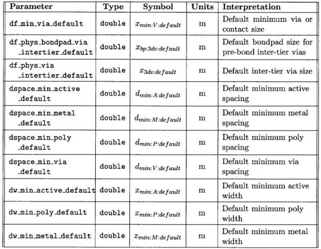
Parameter Type Symbol Units Interpretation
Default minimum via or df -ninvia-def ault double xmin:V:default m conact sie
contact size
df _phys-bondpad-via Default bondpad size for
dfntertier-def
ault pre-bond inter-tier vias
dfiphydvia double X3dv:default
m Default inter-tier via size Aintert ier-def ault
dspace-minactive double d m Default minimum active
_def ault spacing
dspace-ninmetal double d* Default minimum metal
-default spacing
dspace-min-poly double d m Default minimum poly
_def ault spacing
dspace-min-via double d m Default minimum via
-def ault spacing
dw-minactive-def ault double Xmin:A:default m Default minimum active width
dw-min-poly-def ault double Xmin:P:default m Default minimum poly width
Default minimum metal
dw-in-metal-default double xmin:M:default m Dt
width
Table 3.3: Process parameters relating to default widths and spacings for certain
Parameter Type Symbol Units Interpretation
Minimum bondpad size for
df -min..bondpad..
via.intertierX double min:bp:3DvX m inter-tier via X (pre-bond
dfvia.intertierjl dul bp3v ntrte i pebn
process)
df -pys-bodpadPhysical bondpad size for -vi-iteti.- double -Tbp:3Dx In inter-tier via X (pre-bond
process)
Inter-tier via X physical feature sizes (For pre-bond vias, first element is for via from bondpad to landing dfphys-via vector (X3DvXai on tier X+1, second
ele-I m IeIeiL is IOr via irom DOII0
-_intertierX <double> X3DvXbl nit 1
pad to landing on tier X. For post-bond, first element is litho-defined via cut, sec-ond element is physical cut in masking metal.)
dspace-min-bondpad Minimum spacing for bond-_viaintertierX pads of inter-tier via X
vector Vector of minimum spac-dspace-min-levelsTX <double> dmin:tx m ings for corresponding
lev-els in k-levlev-elsTX
Buried oxide thickness on
dt..boxTX double XbOX:tX m .
tier X
dt-overglassTX double Xoverglass:tX m Overglass thickness on tier
X
vector Vector of minimum widths dw-min-levelsTX <double> Xmin:tX m for corresponding levels in
k-levels-TX
vector Vector of pairs indicating
relative z location of top
loc-levelsTX <vector Zlevels:tx m
<double>> and bottom of each level in k-levelsTX

![Figure 2-2: Structure of the GTX framework [11]](https://thumb-eu.123doks.com/thumbv2/123doknet/14733140.573507/33.918.131.691.115.342/figure-structure-gtx-framework.webp)