HAL Id: hal-00469645
https://hal.archives-ouvertes.fr/hal-00469645
Submitted on 24 Jan 2020
HAL is a multi-disciplinary open access
archive for the deposit and dissemination of
sci-entific research documents, whether they are
pub-lished or not. The documents may come from
teaching and research institutions in France or
abroad, or from public or private research centers.
L’archive ouverte pluridisciplinaire HAL, est
destinée au dépôt et à la diffusion de documents
scientifiques de niveau recherche, publiés ou non,
émanant des établissements d’enseignement et de
recherche français ou étrangers, des laboratoires
publics ou privés.
ultra-flexible micromachined polydimethylsiloxane
(PDMS) polymer
S. Hage-Ali, N. Tiercelin, P. Coquet, R. Sauleau, H. Fujita, V.
Preobrazhensky, P. Pernod
To cite this version:
S. Hage-Ali, N. Tiercelin, P. Coquet, R. Sauleau, H. Fujita, et al.. A millimeter-wave microstrip
antenna array on ultra-flexible micromachined polydimethylsiloxane (PDMS) polymer. IEEE
An-tennas and Wireless Propagation Letters, Institute of Electrical and Electronics Engineers, 2009, 8,
pp.1306-1309. �10.1109/LAWP.2009.2037590�. �hal-00469645�
.
Abstract — The use of Polydimethylsiloxane (PDMS), an ultra flexible polymer, as a substrate for the realization of reconfigurable microwave devices in the 60-GHz band is presented. As bulk PDMS is demonstrated to be lossy at millimeter waves, membrane-supported devices are considered. A new reliable and robust technological process has been developped to micromachine membrane-supported transmission lines and microstrip antenna arrays. It is shown that transmission lines printed on 20-µm thick membranes exhibit similar performances as bulk substrates commonly used at millimeter-wave frequencies. A microstrip antenna array has been also designed and fabricated to demonstrate the feasibility of directive antennas supported by large membranes. Promising applications for mechanical beam-steering, beam forming and frequency tunable antennas are expected.
Index Terms— Flexible polymer, Membrane, Polydimethylsiloxane (PDMS), Reconfigurable antennas.
I. INTRODUCTION
here is an increasing need for reconfigurable and deformable antennas for high-speed wireless communications and high-resolution sensing systems at millimeter waves [1]. Multipoint wireless indoor communications, automotive radars, target acquisition systems or wireless sensor networks require specific features for the antenna such as beam-steering, beam-forming, polarization diversity and tunability. For beam-steering applications, mechanically tunable antennas [2] have gained a strong attention because they offer unique features like controllability of the beam direction, nearly constant gain and reduced cost, while usual beam-steering strategies involving phased-array antennas or switched beam antennas face high cost, high loss and complexity issues in the 60-GHz band.
One of the key issues for elaborating mechanically reconfigurable antennas at millimeter waves consists in finding dielectric substrates with suitable electromagnetic and Manuscript received Jun. 19, 2009, revised Oct. 12, 2009. This work was supported partly by the French Délégation Générale pour l’Armement (DGA). S. Hage-Ali, N. Tiercelin, P. Coquet, V. Preobrazhensky, and P. Pernod are with Joint European Laboratory LEMAC, IEMN UMR CNRS 8520, ECLille and Université des Sciences et Technologies de Lille, 59651 Villeneuve d’Ascq, France. (e-mail: [email protected] ).
R. Sauleau is with the Institut d’Electronique et de Télécommunications de Rennes (IETR), UMR CNRS 6164, Université de Rennes 1, 35042 Rennes cedex, France.
H. Fujita is with the Institute of Industrial Science (IIS), The University of Tokyo, 4-6-1 Komaba, Meguro-ku, Tokyo 153-8505, Japan.
mechanical properties. Reconfigurable antennas based on Kapton polyimide (EYoung=5.5 GPa) [3], benzocyclobutene
(BCB) (EYoung=2.9 GPa) [2] and Liquid Crystal Polymer
(EYoung=2.5 GPa) [4] were reported. In this work we propose to
use Polydimethylsiloxane (PDMS), an extremely flexible polymer with a very low Young’s modulus (EYoung=2 MPa)
and which is compatible with many silicon micromachining techniques. PDMS exhibits many attractive features: it is low-cost, light-weight, biocompatible and chemically resistant. It can be formed to any size or thickness down to a few micrometers by spin coating or replica molding [5]. In addition its flexibility enables one to conform it to any shape and to fabricate multilayered structures by simple bonding techniques [6]. In a previous work [7], some of the authors demonstrated the technological feasibility of PDMS membranes as millimeter-wave antenna substrates for a single patch antenna. Several reliability issues arose when trying to fabricate larger membranes for patch array antennas using that process. Here we introduce an improved technological process with enhanced reliability, and we report results obtained on large membrane antenna arrays.
In this paper, we first study numerically and experimentally the insertion loss of transmission lines (TLs) printed on bulk PDMS and PDMS membranes (Section II). The corresponding fabrication process is then described in Section III and applied to fabricate a 4×2 element microstrip antenna array printed on a 20-µm thick and 21.5mm×10.3mm wide self-supported PDMS membrane (Section IV.A). The impedance and radiation characteristics of this array are discussed in Sections IV.B and IV.C, respectively. Conclusions and perspectives are given in Section V.
II. INSERTION LOSS OF TRANSMISSION LINES PRINTED ON BULK PDMS AND PDMSMEMBRANES
The dielectric properties (εr=2.68, tanδ=0.04) of PDMS
(Dow Corning’s Sylgard 184TM) have been measured in W-band using a quasi-optical measurement system [7]. Here microstrip TLs matched to 50 Ω and printed on bulk PDMS and PDMS membranes (Figs. 1a, 1b, and 1c) are studied numerically and experimentally to evaluate the potential interest of PDMS as a dielectric substrate in the 60-GHz band. Their insertion losses were computed using HFSS commercial software and measured with a V-band Anritsu Universal test
A Millimeter-Wave Microstrip Antenna Array
on Ultra Flexible Micromachined
Polydimethylsiloxane (PDMS) Polymer
Sami Hage-Ali, Student Member, IEEE, Nicolas Tiercelin, Philippe Coquet, Ronan Sauleau, Senior
Member, IEEE, Hiroyuki Fujita, Member, IEEE, Vladimir Preobrazhensky, and Philippe Pernod
fixture 3680V (Fig. 1b) connected to an Agilent E8361A network analyzer with TRL calibration. The simulated and measured insertion losses per unit-length are shown in Fig. 2 from 50 GHz to 60 GHz.
(a)
(b) (c)
Fig. 1. (a) Schematic view of 50-Ω transmission lines printed on bulk PDMS and PDMS membranes. H=200µm, h=20µm, W1=540µm, W2=931µm,
L=2mm, εr=2.68 and tanδ=0.04. (b) Bulk PDMS transmission line in the impedance measurement setup based on an Anritsu Universal test fixture 3680V. (c) 50-Ω transmission line on a PDMS membrane.
Fig. 2. Measured and computed insertion loss of 50-Ω transmission lines printed on bulk PDMS and 20 µm thick PDMS membranes. Bulk PDMS: HFSS simulation; Experiment. PDMS membrane: HFSS simulation; Experiment.
These results show that the insertion loss of TLs fabricated on bulk PDMS reaches about 3dB/cm in the 60-GHz band, which is not acceptable for the fabrication of printed antenna arrays and feed networks. Thus a new membrane technology has been developed to overcome this limitation and demonstrate the promising features of micromachined PDMS substrates. To this end, a set of TL supported by a 20µm-thick PDMS membrane has been fabricated using the microfabrication process described in Section III. In this case, in the 60 GHz band, the measured insertion loss drops down to about 0.5dB/cm, a value comparable to the insertion loss of TLs on RT/Duroid 5880 (≈0.45dB/cm) but higher than that of TLs printed on fused quartz substrates (≈0.20dB/cm). Insertion loss can be reduced by decreasing the membrane thickness but
at the expense of the mechanical robustness of the membrane. A 20µm-thick membrane appears to be a good compromise.
III. TECHNOLOGICAL FABRICATION PROCESS
Fabricating thick (1.5µm) and high quality metal patterns on PDMS is a technological challenge because PDMS exhibits a very high thermal expansion coefficient (α=9×10⁻⁴ K-1) and weak adhesion to metal [8] [9]. This explains why PDMS is not suitable for direct metallization by conventional evaporation and sputtering techniques. Consequently we have elaborated a new metal transfer process from a silicon wafer to the PDMS substrate with a specific adhesion layer. This process overcomes the aforesaid technological issues and allows the manufacturing of metal patterns on PDMS with any size, shape or thickness with a high quality and micron-scale resolution.
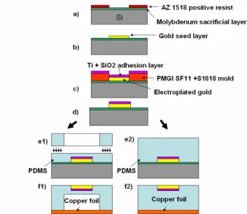
Fig. 3. Main technological steps for manufacturing microstrip lines and planar antennas printed on PDMS membrane (e1 and f1 steps) and bulk PDMS (e2 and f2 steps).
The main technological fabrication steps are described in Fig. 3. The process flows for PDMS membranes (e1 and f1
steps) and bulk PDMS (e2 and f2 steps) structures are similar
until step d. First a 100-nm molybdenum sacrificial layer is deposited on a 3’’ silicon wafer, followed by the patterning of a AZ1518 resist layer by photolithography using the mask defining the shape of the device (step a). Then a 20-nm gold seed layer is deposited by evaporation and patterned by lift-off (step b). During step c, a mold formed with PMGI SF11 and S1818 photo-resists is fabricated by photolithography and a 1.5µm-thick gold layer is electroplated on top of the seed layer. Two adhesion layers (sputtered nm Ti layer, and 50-nm SiO2 layer deposited by PECVD) are fabricated and
patterned by lift-off (step d). For the membrane process (steps
e1 and f1), a 20µm-thick PDMS membrane is first spin-coated
on the wafer. After UV-Ozone activation, a 180-µm PDMS frame, which is hollowed out to form an air cavity, is bonded on the structure. For the bulk PDMS case (steps e2 and f2), a 30 mm
200-µm PDMS layer is spin-coated and baked on the silicon wafer at 110°C for one hour. The molybdenum sacrificial layer is then etched by hydrogen peroxide (H2O2), and the structure
released. Finally the device is placed on a thin copper foil serving as microstrip ground plane (steps f1 and f2).
IV. MICROSTRIP ANTENNA ARRAY ON PDMS MEMBRANE
A. Design
A 4×2 elements microstrip antenna array supported by a 20-µm thick PDMS membrane has been designed. Its layout and 3-D view are represented in Figs. 4a and 4b, respectively. The array is fed by a 50-Ω microstrip line, first printed on a long bulk PDMS section (length L3 in Fig. 4a), then on the
membrane. A taper section has been optimized (length L2 in
Fig. 4a) to minimize the return loss. The radiating elements are entirely supported by a large PDMS membrane (21.5mm×10.3mm). Due to the elastic properties of the PDMS, the membrane is easily stretched by pulling the structure above the ground plane, in contrast to other membrane-based technologies where mechanical stress has to be optimized [10]. As shown in zoomed part of Fig. 4a, each discontinuity is slightly rounded to avoid stress concentration in the gold metallization, which could lead to microcracks. The fabricated prototype is shown in Fig. 4c.
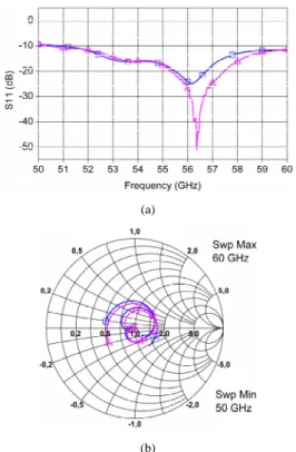
B. Impedance measurements
The return loss and input impedance of the antenna prototype were computed using HFSS and measured in the 50-60 GHz band (Figs. 5a. and 5b.) after TRL calibration. The antenna is well matched at resonance, and the agreement between experiments and simulations is excellent: the relative shift between the predicted (56.2 GHz) and measured (56.3 GHz) resonance frequencies is less than 0.2%.
C. Gain and radiation patterns measurements
The radiation patterns and gain were measured in a far-field millimeter-wave anechoic chamber. When measuring the radiation performance, a V-type connector and a WR-15 waveguide-to-coaxial transition were used. Under these conditions, a maximum gain of 12.3 dBi was found at around 55 GHz, which leads to a radiation efficiency of 28% (the theoretical directivity is 17.7 dBi). This low value is due to the 14.7mm long feed line (L3) printed on bulk PDMS, which
lowers the gain by about 4.1dB. If we consider a feeding scheme fully supported on membrane, with a section L3
supported on membrane and no L2 taper section, the antenna
gain would reach: 12.3 dB + [(2.8-0.5)×1.47] dB + 0.7 dB = 16.38 dB, where 12.3 dB is the measured gain of the fabricated antenna, 2.8 dB/cm and 0.5 dB/cm are the insertion loss per unit-length of bulk PDMS and membrane-supported transmission lines at 55 GHz respectively, 1.47 cm is the length of section L3, 0.7 dB is the HFSS-simulated loss in
section L2 taper. The antenna radiation efficiency would reach
74 %, which is comparable to values obtained on bulk fused quartz [11].
(a)
(b) (c)
Fig. 4. (a) Layout of the microstrip antenna array supported by a PDMS membrane and zoom to see rounded angles. Lacc=4544µm, L2=470µm,
L3=14732µm, Lgap=1855µm, Lp=3100µm, Wp=2225µm, Wgap=1600,
Wacc=170µm, W3=540µm. (b) 3-D schematic of the antenna array (c) Photograph of the fabricated prototype.
(a)
(b)
Fig. 5. (a) Reflection coefficient and (b) input impedance of the antenna array. : HFSS simulation. : Experiment.
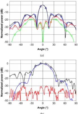
The measured and computed radiation patterns at 55 GHz are represented in H- and E-planes in Figs. 5a and 5b, respectively. The agreement between experiments and simulations is excellent in H-plane. The cross-polarization level at broadside is lower than -32dB. The pronounced ripples observed in E-plane are due to reflection and diffraction effects on the feed connector.
zoom
z y x
(a)
(b)
Fig. 6. Measured and computed radiation patterns of the membrane supported microstrip antenna array at 55 GHz. (a) H-plane, (b) E-plane. : Measured co-polarization component. Computed co-polarization component. : Measured cross-polarization component. : Computed cross-polarization component.
D. Mechanical and thermal stability of the antenna
As mentionned in Section IV.A, PDMS membranes are stretched above the ground plane, which makes them reasonably flat and stable. Optical profilometry characterizations have shown that the total thickness H was varying between 185µm and 210 µm, corresponding to a -7.5%/+5% dimensional variation with respect to the nominal design value H=200µm. The corresponding impact of these geometrical variations is a ± 0.2% resonance frequency shift and negligible differences on the antenna bandwidth and radiation patterns, leading to the conclusion that small variations of the membrane structure in the z-direction are not very critical for the characteristics of the antenna. Thermal dilatation caused by the high thermal expansion coefficient (α=9×10⁻⁴ K-1), 3.6% for 40K for example, may lead to inadequate membrane bending. In this case prestretching the membrane during the manufacturing can compensate future thermal dilatation.
V. CONCLUSIONS AND PERSPECTIVES
A new microfabrication process for millimeter-wave microstrip antennas printed on micromachined PDMS substrates has been elaborated, implemented and validated. The insertion loss of microstrip lines fabricated on 20µm-thick membranes is about 0.5dB/cm at 60 GHz. A 4×2 patch antenna array supported by a large ultra flexible PDMS membrane has been fabricated and fully characterized in impedance, gain and radiation patterns. A very good
agreement between measurements and simulations has been obtained.
Large membranes were easily fabricated using the proposed microfabrication process. The very high softness of PDMS material coupled to MEMS actuators recently developed in [12] is extremely promising for the design of mechanical wide angle beam-steering, beam-forming and frequency tunable antennas.
ACKNOWLEDGMENT
The authors would like to thank the IEMN and IETR technical staff (Laurent Le Coq) for the experimental characterization in impedance and radiation, respectively.
REFERENCES
[1] J. T. Bernhard, “Reconfigurable antennas,” Encyclopedia of RF and
Microwave Engineering, Ed. K. Chang (New York: Wiley), 2005.
[2] W. Baek, S. Song, J-H. Park, S. Lee, J-M. Kim, W. Choi, C. Cheon, Y-K Y-Kim, and Y. Y-Kwon, “A V-band micromachined 2-D beam steering antenna driven by magnetic force with polymer-based hinges,” IEEE
Trans. Microwave Theory Tech., vol. 51, no. 1, pp. 325–331, Jan. 2003.
[3] R. Goteti, R. Jackson, and R. Ramadoss, “MEMS-based frequency switchable microstrip patch antenna fabricated using printed circuit processing techniques,” IEEE Antennas and Wireless Propag. Lett., vol. 5, pp. 228–230, 2006.
[4] G. DeJean, R. Bairavasubramanian, D. Thompson, G. E. Ponchack, M. M. Tentzeris, and J. Papapolymerou, “Liquid crystal polymer (LCP): a new organic material for the development of multilayer dual-frequency/dual-polarization flexible antennas arrays,” IEEE Antennas
Wirel. Propag. Lett., vol. 4, pp. 22–26, 2005.
[5] J. C. McDonald, D. C. Duffy, J. R. Anderson, D. T. Chiu, H. Wu, O. Schueller, and G. Whitesides, “Fabrication of microfluidic systems in poly(dimethylsiloxane),” Rev. Electrophoresis, vol. 21, pp. 27–40, 2000.
[6] B.-H. Jo, L. Van Lerberghe, K. Motsegood, and D. Beebe, “Three-dimensional micro-channel fabrication in polydimethylsiloxane (PDMS) elastomer,”J. Microelectromech. Syst., vol. 9, pp. 76–81, 2000.
[7] N. Tiercelin, Ph. Coquet, R. Sauleau, V. Senez, and H. Fujita, “PolyDiMethylSiloxane membranes for millimeter-wave planar ultra flexible antennas,” J. Micromech. Microeng., vol. 16, pp. 2389–2395, 2006.
[8] N. Bowden, S. Brittain, A. G. Evans, J. W. Hutchinson, and G. M. Whitesides, “Spontaneous formation of ordered structures in thin films of metals supported on an elastomeric polymer,” Nature, vol. 393, no. 6681, pp. 146–149, May 1998.
[9] H. Schmid, H. Wolf, R. Allenspach, H. Riel, S. Karg, B. Michel, and E. Delamarche, “Preparation of metallic films on elastomeric stamps and their application for contact processing and contact printing,” Adv.
Funct. Mater., vol. 13, no. 2, pp. 145–153, 2003.
[10] M. Stotz, G. Gottwald, H. Haspeklo, and J. Wenger, “Planar millimeter-wave antennas using SiNx-membranes on GaAs,” IEEE Trans.
Microwave Theory Tech., vol. 44, no. 9, pp. 1593-1595, Sept. 1996.
[11] Ph. Coquet, R. Sauleau, K. Shinohara, and T. Matsui, “Multi-layer microstrip antennas on quartz substrates. Technological considerations and performance at 60 GHz,” Microwave and Optical Technology
Letters, vol. 40, no. 1, pp. 41–47, Jan. 2004.
[12] P. Pernod, V. Preobrazhensky, A. Merlen, O. Ducloux, A. Talbi, L. Gimeno, R. Viard, and N. Tiercelin, “MEMS magneto-mechanical microvalves (MMMS) for aerodynamic active flow control,” J. Magn.