Analysis and Design of Regular Structures
for Robust Dynamic Fault Testability
The MIT Faculty has made this article openly available. Please share how this access benefits you. Your story matters.
Citation Bryan, Michael J., Srinivas Devadas, and Kurt Keutzer. “Analysis and
Design of Regular Structures for Robust Dynamic Fault Testability.” VLSI Design 1, no. 1 (1993): 45–60. © 1993 Hindawi Publishing Corporation
As Published http://dx.doi.org/10.1155/1993/38536
Publisher Hindawi Publishing Corporation
Version Final published version
Citable link http://hdl.handle.net/1721.1/96136
Terms of Use Creative Commons Attribution
1993, Vol. 1,No. 1,pp.45-60
Reprintsavailabledirectlyfrom the publisher Photocopying permitted bylicenseonly
Printed in the UnitedStatesof America
Analysis and
Design
of
Regular
Structures
for Robust
Dynamic
Fault
Testability
MICHAEL J. BRYAN
and
SRINIVAS DEVADAS
DepartmentofEECS, MITCambridge, Massachusetts,USA
KURT
KEUTZER
Synopsys, Mountain View, California, USA
Recent methods ofsynthesizing logicthat isfullyandrobustlytestable for dynamic faults, namely path delay,
transistorstuck-openand gatedelayfaults,relyalmostexclusivelyonflattening given logic expressionsinto sum-of-products form,minimizingthe covertoobtaina fully dynamic-faulttestabletwo-levelrepresentation of the functions, andperformingstructural transformationstoresynthesizethecircuit into a multilevel network, while also maintainingfulldynamic-fault testability. Whilethistechniquewillwork well forrandomorcontrol logic,
itis not practical formany regularstructures.
Todeal with thesynthesisofregularstructures fordynamic-fault testability,we present amethodthat involves thedevelopmentof a library of cells for theseregularstructuressuch thatthecellsareallfully path-delay-fault, transistor stuck-open fault orgate-delay-fault testable. Thesecells can thenbe utilizedwheneveroneof these standard functionsisencountered.
We analyzevariousregularstructures such as adders,arithmeticlogicunits,comparators, multipliers,andparity generatorstodetermine iftheyaretestable fordynamicfaults, or howtheycan be modifiedtobetestable for dynamicfaults while still maintaining goodarea andperformancecharacteristics. Inadditiontominimizing the area anddelay, anotherkeyconsideration istoget designswhichcanbe scaledtoan arbitrary numberof bits while still maintainingcomplete testability. In each case, the emphasis is onobtaining circuits which are fully path-delay-fault testable. Intheprocessofdesignmodificationtoproduce fully robustlytestable structures, we have derived a number ofnewcompositionrules that allow cascading individualmoduleswhilemaintainingrobust testabilityunderdynamicfault models.
KeyWords: Synthesisfortestability; Dynamicfaults;Regularstructures; Compositionrules
ecentmethods ofsynthesizing logicthatisfully
testablefor dynamicfaults, namely path delay,
transistor stuck-open and gate delay faults (e.g.
Kundu and Reddy, and Kundu et al.
[6, 7]),
relyalmost exclusively on flattening given logic
expres-sions into sum-of-products form, minimizing the
cover to obtain a fully dynamic-fault testable
two-level representationofthe functions, andperforming
structural transformationstoresynthesize thecircuit into a multilevelnetwork,whilealso maintaining full dynamic-fault testability. While this technique will
work well for randomorcontrol logic,it is not
prac-tical for many regular structures.
Thereare twomajorproblemswithapplyingthese synthesis techniquesto.regular structures. First, for
manyof thesetypeof circuits, the number ofproduct
terms intheflattenedstructurebecomes prohibitive.
Consider abinaryadderas anexample.
In
anadder, the number ,ofproduct
terms grows exponentiallywiththe number ofbits.
For
anN-bitadder, themostsignificantbitof thesumoutputhas 2u+2 4product
terms in its flattened representation. Another
ex-ample is aparity generator.
An
N-bit paritygener-ator has 2N-1
product
terms in the flattened repre-sentation ofthecircuit.As
aresult ofthisexponentialgrowthinthe number ofproductterms,itcanquickly
become prohibitive in terms of both the CPU time
required and the memory requirements to flatten even relatively smallregularstructuressuchasadders andparitygenerators.
A
second problemisthat inflatteningthe original logic expressions, the structure that the designer has created in the overall architecture is lost. This canresult in a number ofproblems if the optimization
algorithms cannot synthesize an implementation
which has similar area or performance
characteris-tics, which is often the case for regular structures.
For example, often a bit-slice approach works best for many data path structures. The basic building block can be optimized and laid out, and then the overall circuity constructedbysimply replicatingthis one block many times. Once the structure is flat-tened,all oftheinformationabout the
original
struc-tureislostwhichmaynotbe recoverablebysynthesisprocedures.
As a result of the problems identified with trying
toflatten regular structures and then synthesizing a
dynamic-fault testable implementation,it isdesirable
to develop an alternative method for dealing with such circuits. In Devadas and
Keutzer
[4]
a simple composition rule for robustly path-delay-faulttest-able circuits was developedthatallowed for the
de-velopmentofarobustly path-delayfaulttestable
rip-ple-carry-adderand aparity generator.
A
number ofnew compositionrules are developed here in order
to develop alibrary of cells for theseregular
struc-tures which are allfullydynamic-fault testablewhich canthen beutilizedwheneveroneof these standard
functions isencountered.
The following sections use and extend thetheory
ofDevadas and Keutzer
[3,
4]
tocreate alibrary ofregular structures suchas avariety ofadders, arith-meticlogic units, comparators, multipliers, and
par-ity generators. The theory is used to determine if
common structures are testablefor dynamic faults,
orhowtheycanbe
modified
tobe testablefor
dynamicfaults
while stillmaintaininggoodareaandperform-ance characteristics. In addition to minimizing area anddelay,anotherkeyconsideration istogetdesigns
which can be scaled to an arbitrary number of bits while stillmaintaining completetestabilityfordelay
faults. Ineach section, the emphasisis onobtaining
circuits whicharefully robustly path-delay-fault
test-able.Thisimpliesthattheyarefully robustlytestable forgate-delay-faultsandstuck-openfaults as well
[3].
When this is not achievable withoutsignificantarea or speed penalties, methods of obtaining transistorstuck-open-fault testable and robustly
gate-delay-fault testablecircuits are analyzed.
PREVIOUS
WORK
Because
oftheimportanceofregulararithmetic and logical structures in digital design, anumber ofre-searchershavesoughttodeveloptesting methods for these structures, but most of the attention has
ap-parently been focussed on functional testing
(for
asurvey see Abramovici et al.
[1]
chapter8).
These functional tests areusefulindetecting faults that af-fectthe logicalbehaviorof circuits, but they donotaddress the temporal behavior of the circuit.
Fur-thermore, many implementations of regular struc-tureswhich arecompletelytestable functionally,may
bepoorlytestable for faults suchaspath-delay-faults,
even when the functionalvectors can be applied at speed.
Inlight of this,if there is interestindetectingdelay
faults then attention must be given to the precise
logic-gate-level implementation of regular logic
structures. The testability of transistor-level design ofarithmeticregularstructures isconsideredin
Mon-toye
[8].
Unfortunately, delay defects are notex-plicitly considered there and the results are tied to
particular transistor structures in an nMOS custom
designmethodology.
DEFINITIONS
A
gate has an input/output stuck-at-1 if the logicalvalue associated with the input/outputis 1
indepen-dentlyof the valuepresented atthe input. Stuck-at-0 can be defined similarly. If a fault is stuck-at-1 untestable then the input net or gate in the circuit associated with that faultcan be
replaced
by acon-stant 1. Similarly for stuck-at-0.
A
circuithasagate delayfault if thereisonegatein the circuit such that the output of the circuit is slow to make a 0--> 1
(or
1 --->0)
transition even whenone or moreofthegate’s
inputschangevalues.Eachsingle gate delayfault is assumedtobe so
cat-astrophicas tocause a delay along any path to any
output.
A
gate in a CMOS circuit has a transistorstuck-open fault ifthere is one transistor in the gate that
is permanently non-conducting.
A
circuit has a path delay fault if there exists apathfrom aprimaryinputto a primaryoutputviaa set ofgates andinterconnectingnetssuch that a
pri-maryinputevent isslow topropagate alongthepath
to the primary output.
Necessary
andsufficient conditionsforpath-delay-fault testability weregiven inDevadas and
Keutzer
[3].
Inorder for agatedelayfaultto be detected, it is sufficientforapath throughthe gatetoberobustlytestable. Similarly,inorder forastuck-openfaultat
the inputofagate tobe detected, it issufficient for
apath throughthat input to be robustlytestable.
A
robusttest foradynamic(gate
delay,transistorunder arbitrary delays and is therefore not
invali-datedbyhazards orraces.
Throughoutthispaperwewillassumethatarobust
testfor a dynamic fault inacircuit Cis a vectorpair
(v, v2)such
thatC(v)
0 andC(v2)
1. Let theexpectedtransitiontime onthevectorpairbe z. The
applicationof thevectorpairisasfollows: VectorVl
is applied to C and the values on nets are allowed
to settle for an arbitrary amount oftime. Vector v2
is then applied to C. At time
"
the output of C issampled; ifthe value is 1 then no fault isdetected,
otherwise a fault is detected.
Next,
the vector pair(v2, v)
is applied to propagate the opposite eventalongthepathand detect faults correspondingtothe 1
-
0event.ADDERS
There are numerous types of adder designs which
providevariousperformanceandareatradeoffs.We
have analyzedvariousadderstructurestodetermine iftheyaretestable for thevariousclasses of dynamic faults, or how they can be made to be testable for these classes of faults. Since data path structures
oftenform the criticalpathin asystem,it isimportant
that these paths be testable for delay. We will not describe the analysis in its entirety
(the
reader isreferredto
Bryan
[2])
butwillsimplypresentanoveldesign ofacarry bypassadderwhich isfullytestable for path delayfaults.
The composition rule below was proved in
De-vadas and
Keutzer
[4].
All of thecircuitimplementationsin thispaperare
given in terms of AND gates, OR gates, and
in-verting buffers, as wellas exclusive ORgateswhich aremodeledusingthese threetypesofgates.
In
someof the cases the inverters are not explicitly
repre-sented in the logic diagrams, but are impliedby in-versionbubblesontheinputsoroutputsof theother gates.
In
the actual models these inverters must beexplicitly represented in order to accurately
repre-sent all possible gate delay faults. Describing the
circuits in this manner provides a good method to
easilyanalyzewhether theimplementationistestable for robust path-delay-faults as well as the other classes of dynamic faults. Thepathsinanactual
tran-sistor-level implementation in a particular
technol-ogyand designstyle
(such
asstaticCMOS)
willhavea one-to-onecorrespondencetothepathsinthe gate-level implementations usedin thispaper.
The carry lookahead and bypass adders create
both the propagate
(P)
and generate(G)
terms for each bit. The propagate term is asserted whenevera carry input would propagate through the adder
section based on the values of the operands. Thus for a 1-bitsection, P
A
B. Thegenerate term isassertedwheneveracarryisgenerated byanaddersectionbasedononlythe valuesoftheoperands
(i.e.
regardlessof thevalue of thecarry input). Thusfor a 1-bitsection, G
A
B. Thecarry outputwhich iscreated from the propagate and generateterms is defined as CO G+
P
CI.In
Figurel(a),
thestandard logic for generating the propagate,
gener-ate, and sum outputs for each bit is shown.
An
al-ternate representationisshown in Figurel(b).
Composition Rule: Given a setof
robustlypath-delay-faulttestablecircuits, C1, C2,
CN,
if
for
1<-<
Nasingle outputof
Ci,namelyli
feeds
Ci+
andfor
1 <- i, <- Nwhen j the inputsof C
andC
are disjoint, then the composition is fully robustly path-delay-faulttestable.
Carry
Bypass
AdderThecarry bypassadderisjustanoffshoot of thecarry
lookahead adder. It becomesvery inefficient to
ex-tend thecarrygeneration scheme for lookahead
ad-A
(a)Conventional Implementation (b)AlternateImplementation
4-bitadder 4-bitadder A S S{4:7} B(0:3) G B G Cl Cl P
Cl,
P COFIGURE 2 Carrybypass adderimplementation.
ders to very large bit-widths. Typically, the carry
signals are only calculated in this mannerfor up to 4-bit sections.
By
creatingapropagateandgenerate signal foreach4-bit section, the carry signal canbebypassed through each stage as shown in Figure 2. The logic for thecumulativepropagateand generate signal for each 4-bitstage can beexpressedin terms ofthe propagate and generate signals for each bit, where P P0. P1. P2. P3 and G G3
+
G2. P3+
G1 P3. P2+
GO. P3. P2. P1. Animple-mentation isshown inFigure3.Usingacarrybypass
scheme allows eachN-bitstage
(4-bit
in thiscase)
tobe identical, and thus makes layout simpler since
only one stage needs to be laid out, and then an
arbitrary number of these blocks can be
intercon-nectedto form alarger adder..
The carry bypass generation is an algebraic
fac-torizationofthecarrysignal.Thiscircuit isthusfully
testable assuming thatthe individual propagate sig-nals for each bit are implemented as
P
A+
B,
i.e. the alternate implementationofFigure
l(b).
If the propagate signalisimplementedasP
A
(B,
then the circuit will not be fullytestable.
For a 28-bit carry select adder composed of7
4-bit stages, the longest path for a carry select adder would be 10 stages of logic
(each
stage being twolevels).
For
the carry bypass adder, the worst casedelay for the carry output signal would be 8 stages
of logics7 carry bypass chains and the propagate/
generatelogicinthe firststage. The worstcase sum
output would go through10stages oflogics6upto
the carry input of the last stage, and 4 in the last
stageoftheaddertogenerate the sums (assuming a
Note that the commonly used implementation of the carry bypassadder has a single stuck-at faultredundancy. Removing this stuck-at faultredundancyresults ina circuit that is consid-erablyslower than theoriginalcircuit. In Keutzeretal. [5],an implementationof acarry bypassadder that wasfullytestable for stuck-atfaults withequalorbetterperformancethan the redun-dant adder wasgiven.However,the circuit ofKeutzeretal. [5]
was notfully robustly path-delay-faulttestable. The circuit
pre-sented hereiscompletely robustly path-delay-faulttestable, and maintainstheperformanceof the original circuit.
ripple
adder).
By
adjusting the stage size, theper-formance of thecarry bypass addercan be made to
exceed that of the carry select adder.
However,
thesignificantadvantageof thecarry bypassadderis that it does not need to generate two different sums at
each stage and then multiplex the outputs, creating
a large savingsin area.
Summary
of Testability ofAddersItwasshown
[2]
thatall fourtypesofaddersanalyzedcan be madetobe fullytestable forall threeclasses
ofdynamic faults. It was also shown that the carry
select adder becomes inferior to the carry bypass
adder andhas nosignificant advantageswhichwould resultin itbeing chosen over thecarry bypassadder..
While versions ofthecarrylookahead andcarry by-pass adder were shown that are fully testable, the
mostcommonlyusedimplementationofthese adders
isnotfullytestable. The testableversionaddsasmall
amount of logic to the common implementation
(1
OR gate per adder
bit),
but retains the sameper-formance characteristics or improves the
perform-ance slightly. G3 P3 G2 P2 G1 P1 PO FIGURE 3 tion. G
implementa-A>Bin_
A<Bin A-Bin
FIGURE4 1-bit extensiblecomparator implementation.
A>B
A<B
COMPARATORS
Binary magnitude comparators are another type of
regularstructure.
It
is desirable tohaveacomparatorwhich isfullytestablefordynamic faults thatcanalso
bescaledtoan arbitrary number ofbits.Performance
is also an important cost function when evaluating alternate comparator designs.
In
this sectionthetest-ability of some typical comparator implementations and methodstocascade comparators are analyzed.
Ripple
Comparator
An
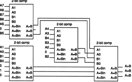
N-bit comparatorcan be constructed by simply connectingN 1-bit extensible comparatorsin series.An
implementationof a 1-bit extensiblecomparatoris shown in Figure 4. It has five inputs, 2 ofwhich are the operands A and
B,
and the remaining threeare theresults ofthe comparison ofthe less signifi-cant bits. The three outputs indicate whether
A
isgreater than, less than, or equal to B. The
imple-mentation showninFigure 4isfully testablefor
dy-namicfaults.
It
has 14gates, 25 links, and 15paths,all ofwhich are robustly testable.
The 1-bit extensible comparator shown in Figure 4 can be cascaded together to form an N-bit
com-parator by simplyconnecting thecomparisonoutputs of the ithstage tothe comparison inputs of the
+
lthstage.A
3-bitripple comparatorisshowninFig-ure 5.
Note
that the first stage has been simplified by using the fact thatA >
B
0,A <
Bg 0, andA
B,
1. The ripplecomparator
is fullytestable forpath delayfaults sinceeach stageisfully
testable and the inputs that affect each output ofa
given stagearefullycontrollable.
Note
that theentireinput set for a given stage isnot fully controllable,
since the inputs
A >
B,
A
<
B;,
andA
B
foragivenstage canonlytakeonthe values
(100),
(010),
or(001).
However,
theoutputA
>
Boftheithstageonly depends on the inputs
A,
B;,
and A> Bi-l.
Thus for
A
> Bi
tobe testable forpath delay faultsonly requires that
A;,
B,
andA>
B;-1 beindepen-dently controllable and that the stage itselfbe fully
testable.
A >
Bg_ isindependentofAgandBg, soA
>
Bisfullytestable.Similarargumentscanbe made forthe outputsA<
B andA B.Figure 5 above indicates a more general
compo-sition rule than the rule given in Devadas and
Keutzer
[4].
Composition Rule: Considera set
of
robustly path-delay-faulttestablecircuits,C,
C2,Cu,
wherefor
1 <-<
Noutputs li!, lipfrom
Ci
feed
Ci+
1, each1-bitcomp
AIB1
0 A<Bin A<B B2._ 1-bitcomp A>Bin A>B A=Bin A=B A<Bin A<BFIGURE5 3-bit ripple comparatorimplementation.
AB A-B
Ci
blockreceivesanothersetof
inputs, namelyI
such thatfor
1 <- i, ] <- N whenL
I
andI
have no commoninputs.If,
for
1 <- <-N, 1 <- k<- P,li
only depends onIi
and li-, then the composition isfully robustly path-delay-fault testable.Each circuit C can be brokenup intoP parallel
cir-cuits, each receiving
Ii
and l_1,. Then, givenCom-position Rule on
Carry
Bypass
Adder, we have the above result.one additional comparator is required. This
com-parator receives as inputs the A
>
B andA <
B outputs ofthe other comparators,with the resultofthe comparison of the most significant input bits
being connected to the most significant bits of the
finalcomparator.
Theparallel comparatorimplementationinFigure 6 is not fully testable for dynamic faults. The
un-testabilityoccurs sincethe
A
andBinputsof the finalcomparatorare not fullycontrollable.
Parallel
Comparator
While anarbitrarysizeripple comparatorcanbe
con-structed, delays become prohibitive when perform-ing comparisons of large operands. An alternate method of performing comparisons ofoperandswith alarge number ofbits is to construct aparallel
com-parator.
A
parallelcomparator oftwo N-bitoperandscanbe constructedoutofN/MM-bit extensible
com-parators. Animplementationof an 8-bitcomparator constructed out of4 2-bit extensible comparatorsis
shown in Figure 6. In this commonly used imple-mentation, the comparatorwith the least significant
bitsof the operandsisconnected inthe typical man-ner.
However,
thecomparatorsthatreceivethe otherbits of the operands can accept one additional bit,
with the operand
Ai
being connected totheA > Bin
input, andthe operand
Bi
being connected totheA<
Bi,input.TheA
B,
inputis tiedlow.In
addition tothe comparatorswhich receivethe primary inputs,Alternate Parallel
Comparator
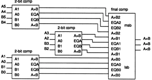
Figure 7 is an alternate method for implementing a
parallel comparator. The comparator in Figure 7 is a 6-bitcomparator, andiscomposedof3initialstages
each of which doesa2-bitcomparison, and then an
output stage which performs the final comparison.
This implementationisfully testable for path delay
faults. It has a total of 85 gates, 187 links, and 144
paths,
all of which arerobustly testable.Figure8shows thedetailedimplementation of the
initial 2-bit stage used intheparallel comparatorof
Figure 7. Thereare4 outputs from each of the
com-parators in the input stage. These outputs areA
>
B,
A< B, EQA,
andEQB.
Output
A>
Bisasserted wherleverA isgreater thanB,
andA < B
isasserted wheneverA
isless thanBfor thebitsof theoperandswhichareinputstothe particularstage.
Output EQA
is the minimalexpression obtainedfrom using
A
B as the
ON-set,
andA >
B as the DC-set. Thus2-bitcomp A6 A0 B7 B1
i_.1
A5A>Bin A>BI 2-bitcomp
0 A-Bin A-B A4 B5 A<Bin A<B
,
A1
2 A>Bin A-Bin B2 A<Bin AI__ AO__ BI__ BO._. 0 0 2-bitomp A1 A0 B1 B0 A>Bin A>B A-Bin A=B A<Bin A<B A>B" A-B A<B" 2-bitcomp A>Bin A=Bin A<BinFIGURE6 8-bitparallel comparator implementation.
A>B A>B
A=B A-B
A5 A1
’A1
A0 A0 B1 B1 B0 B0 2-bitcompA1 A>B finalcomp
B1 EQ A>B2
EQA2
msb B0 A<
2-bitcomp EQB2
A3 A1 A t_,..__. A>B1 A2 A0
EQA
L__. EQA1 B3 B1 EQ EQB12-bitcomp B2 B0 A<
A<B1 A>
B
A>BOEC,_A
EQAO IsbEQBBI
EQBO A< A<BOFIGURE7 Alternateparallel comparator implementation.
A>B A-B A<B
whenever
EQA
is asserted,A is either greater thanorequalto
B,
butEQA
A >_ B. Likewise, output EQBisthe minimal expressionobtainedfrom usingA
B as theON-set,
andA<
B as the DC-set.Thus whenever
EQB
isasserted,Ais eitherlessthanor equalto B.
Figure 9 shows thedetailedimplementationofthe final comparison stageused in.the parallel
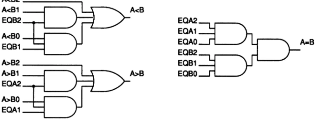
compar-ator of Figure 7. This logic takes as inputs the 4
outputsof each of the input stages and generates the final outputs ofthe comparator. The output
A >
Bis asserted whenever input A
>
Bi
and inputs EQA/:,,_ areasserted,nbeing the numberofinput comparator stages, numbered from0 ton 1. TheEQA
terms canbe considered the equivalentof the propagate terms in the carry lookahead adder. Inorder foran assertion oftheA
> B
outputofagiveninput stagetocause an assertion ofthe
A >
Boutputof the overall circuit, all of the
EQA
terms of themore significant input stages mustbe asserted. The
A
< B
outputis definedsimilarly, with itdependingon the
A
<
B andEQB
inputs. TheA
B
outputisassertedwhenever all of the
EQA
andEQB
inputsareasserted. Figure 7 givesrise tothe following
com-position rule.
Composition Rule: Given a set
of
individuallyro-bustly path-delay-faulttestablecircuits, C1, C2,
CN
A1
B1
A1
B1
FIGURE8 Alternate2-bitcomparatorinitialstage.
A<B
A<B2 A<B1 EQB2 A<B0 EQB1 A>B2 A>B1 EQA2 A>B0 EQA1 EQA2 EQAO_._J-I J
--L"
’
A-B EQB2 / /’--EQB0FIGURE9 Alternatecomparatorfinalstage.
and Dsuch thatC1, C2, CN
feed
D,if
for
1 <- i, j<- N when j the inputs
of C
andC
are disjoint,for
1 <- <- Noutputsli,lie
from
Ci
feed
D, and the side-inputson thepathsinD beginningfrom
anyli
can becontrolledtoO1 by lm, k i, 1 <- rn <- P,then the compositionisfully robustlypath-delay-fault
testable.
Since each
C
is fully testable, a transition through any pathcan bepropagatedto anoutputli.
A
tran-sition on
li
can be propagated through paths inD,
given that the appropriate values can be produced bythe other
C
blocks,that have disjoint inputsfromc.
There are two major disadvantages with this al-ternateparallelcomparator. Thesedisadvantagesare
theextraarearequiredtoimplementthecircuit, and theproblemswhich occurwhenscalingittoalarger
number of bits. For small comparators, the size is
comparable to that of the other comparators
pre-sented.
For
a 3-bit comparator, the ripplecompar-ator, parallel comparator constructed out of ripple comparators,
and
the alternate parallel comparatorwould each have 48literals in their multilevel cover.
However,
for an 8-bit comparator, the size of the first two would scale linearly to 128 literals, whilethe alternate comparatorwould increaseto
approx-imately 220 literals. The testability ofthe alternate comparatorcanbe maintainedforlargerdesigns, but the area penalty becomes increasingly worse. Thus the design does not scalewell. From aperformance
standpoint, the alternateparallelcomparatorisfaster than the originalparallelcomparatorpresented. For
the case ofan 8-bitcomparator, the longest path in
the original comparator would be through
8
gates,while the longest path in the alternate comparator
willbethrough4 gates. Thisadvantageinspeedwill
gradually be lostfor larger comparators.
From a functionalstandpoint, anequivalent
com-parator to that shown in Figure 7 could be
con-structed by generating a single A B output from eachinputcomparatorstage. Thissignal could then
be used inplaceofthe EQA and
EQB
terms inthefinal comparison, with A
>
B only being assertedwheninputsA
> Bi
andABi+
l:n-Iareall asserted.However,
this implementation is not fully testable. Allof the 70gates and 172links arerobustlytestable,but only 144 out of 192 paths are robustly testable.
It can be shown that all 48 untestable paths
corre-spondtostuck-atfault redundancies, andiftheyare
all removed from this comparator implementation,
the circuit of Figure7 would result.
However,
thisdesign does not scale well to generate arbitrarily
large comparators, and in general the design is in-feriorto the otherspresented in this section.
Itisof interest to note thatwhen the comparator
"propagate"
signals EQA and EQB are defined tobe simplyA
B,
this isequivalenttothe case when the propagate signal for the carry lookahead adderwas defined tobe P
A
B. Both of these cases define the propagate signalto allow asignal from a lowerstagetopropagate through onlywhenthesig-nal canpropagatethroughand when the signalis not
generated at the current stage. Both of these cases arealsonotfullytestable forpath delayfaults.
How-ever, when the propagate signal is defined toallow
asignalfrom alower stagetopropagatethrougheven if the signal is generated at the current stage, the circuits both becomefully testable.
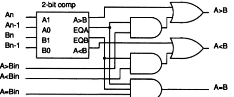
Bypass Comparator
The disadvantage of the parallelcomparator of
Fig-ure7 overthat of Figure 6isthat thecomparatorof
de-An An-1 Bn Bn-1 A>Bin A<Bin A-Bin 2-bitcomp A1 A>B A0 E( B1 E( B0 A<B
FIGURE10 Bypasscomparator.
A>B
A<B
signed and laid out. In addition, it does not scale well, andrequires more area to implement. A
com-paratorwhich isfullytestablefordynamicfaults but
which only requires a single cell type is shown in
Figure 10. This comparator is similar to the carry bypass adder
(see
appropriatesection).
Each stageis composedof a comparatorwhichgenerates theA
> B,
A< B, EQA,
andEQB
signals such as that shown in Figure 8. The stage also receives theA>
B,
AB,
andA<
B signalsfrom the precedingstage, andaddssome additionallogictogenerateA
> B,
A<
B, and A B signals which reflect thetotalresult of the comparisontothat point. Thusno final output stage is needed. The disadvantage is
slower
performance.
In the case of the N-bitcom-parator constructedoutof stages ofM-bitseach, the
longest pathwould be through oneM-bit
compara-tor, and N/M 1 stages of bypass logic. This
im-plementation is, however, much fasterthanthe
rip-ple comparator of said named section. This design does
.require
more areathan the comparatorswhich were notfullytestable, but the area isless thanthat of the comparator of theprevious
section. An 8-bitcomparatorwould have 195literals in themultilevel cover for the circuit. This is about 50% more than for theripplecomparator, butsincetheareaforthis
designscales linearly with the number ofbits ofthe comparator, theareapenaltywillnotgrow anyworse
for largerdesigns.
Comparator Tree
StructureIn
the preceding sections, three fullytestablecom-paratorswerepresented. Each ofthese designs has
someweaknessesassociated with it.The ripple
com-parator has a delay which
grows
linearly with the number ofbitsinthecomparator. Itdoes, however, have a compact area. The alternate parallelcom-parator has a delaywhich is largely independent of the size of the comparator. However, ithas a large
area penalty which becomes increasingly worse for
large comparators. Thebypasscomparator hasa
de-laywhichalsogrowslinearlywiththenumberofbits,
although it is faster by a constant factor than the
ripplecomparator. This increaseinperformance
re-sultsin a 50% increase in area overthe ripple
com-parator.
In
this section, another comparator ispre-sented which has good performance and area
characteristics, but which has somewhat reduced testability.
Iffull robustpath-delay-fault testability isnot
es-sential, a comparator can be constructed which is
fully gate-delayandstuck-openfault testable,has an areaapproximately 30% less thanthatof the ripple comparator, and which has performance
approach-ingthatof theparallel comparator. Ablock diagram of this comparator is shown in Figure 11. It is
im-plemented using a binary tree structure. The input
cells determine if a given bit of the operand A is
greater thanorlessthanthe correspondingbit of the
operand B. The subsequent stages
compare
sets oftwo A
>
B and A<
B signals from the previous level and generate a single pairofA>
B andA <
B signals. This continues until a final result is achieved. The basic cells for this comparator are
shown inFigure 12.
The structure of Figure 11 inspires the following rule. The rule can be used repeatedly to show that
thecomparatortreeisrobustly stuck-openand gate-delay-faulttestable.
Composition Rule: Given a robustly stuck-open
fault
(gate delayfault)
testablecircuit,C,
anda ro-bustlypath-delay-faulttestablecircuitC2
suchthatout-puts 11,
Ip
from
C1
feed
C2,if
a transitioncan berobustly propagated through every link (gate) in
C
tosomeoutput
of
C,
namelyl,
while holding thelk,k j atconstant values that allow the robust
prop-agation
of
this eventthrough somepath in C2, then the composition isfully stuck-openfault
B2, A>B
A1 A<B
B1 A0 B0
FIGURE11 4-bitcomparatortree.
Holding the lk, k jto constant valuesisnecessary
toensurethat the transition on
l
canbepropagated robustly throughC2.
Stuck-openorgate delayfaultsin
C2
can be detected by robustly propagating an event along a path that passes through theappro-priate links or gates.
Thedelay throughthiscomparatorisproportional to log2
N, N
being the number of bits beingcom-pared. Itisalso possibletoimplementasimilar
com-parator using a scheme in which each subsequent
stagecombines theresults of three stages atthe
pre-viouslevel, making thedelay proportionaltolog3 N.
Theareasavingin thisbinarytreecomparator design
isaresult ofnotgeneratinganA Bsignalatevery
level in the design. This signal is
generated
with asingleNORgateatthe output of the circuit, and thus
a30% area improvement can be obtained over the ripple comparator foran 8-bitcomparator
(90
literalsversus 128
literals).
This samepercentageimprove-ment in area is also maintained for larger
compar-ators. Thusthis design scales wellin terms of area,
performance, and testability. The disadvantage is
that it is not fully testable for the most restrictive
class ofdelayfaults,namelyrobustpath-delayfaults.
ARITHMETIC
LOGIC
UNITS
Arithmetic logic units are another type of regular
structure for which it is highly desirable to be fully
testable for dynamic faults sincetheyoften comprise thecriticalpathwithinthe design.Typicallyan
ALU
contains a high degree of shared logic and thus is
generally not fully testable. We refer the reader to
Bryan
[2]
for the analysis and design ofadder/incre-menter circuitsandadder/substractorcircuitsfor
dy-namicfault testability. We summarizethe
composi-tionrulesthatareusefulindesigning suchstructures.
Wedo not restrictthe subcircuits to have disjoint inputsasin the Composition Rule dealingwith
Carry
Bypass
Adder.Composition Rule: Given a set
of
robustly path-delay-fault testable circuits,C,
C2,Cu
such thatfor
1 <-<
Nasingle outputli
of
Ci
feeds
Ci+
andcommon inputs 1, Ip that
feed
all the Ci,if
the remaining inputs toCi
can damp atransition on anyinputlj
before
convergence withpathsfrom
l, then the composition isfullystuck-open
fault
andgate-delay-faulttestable.
Stuck-openfaultscorrespondingto
I
links are prop-agatedtol
orthe outputsofsomeC.
In
the former case, thetransition can bepropagated
throughC+
robustly,sincethetransition onljneverreconverges. We also giveaconditiondifferentfrom the
Com-position Ruleon Arithmetic Logic Units that main-tains testability.
Composition Rule: Given a set
of
robustly path-delay-fault testable circuits, C1, C2,Cu
such that(a)Initialcomparestage
A>B
A>B0
(b)Subsequentcomparestage
FIGURE 12 Comparatortreebasiccells.
for
1 <-<
Nasingle outputli
of
Ci
feeds
Ci+
1, andcommoninputs11,
Ie
thatfeed
all the Ci,if
for
eachCi
(1)alllinksfrom
inputsljinCi
aretestableatsomeoutput
of
Ci
not equal toli
and(2)
a path throughotherlinks in
C
isrobustlytestable up tothe pointof
outputl
orsomeother outputof C
byplacingconstantvalues on the
I,
then the composition isfullygate-delay-faultandstuck-open
fault
testable.Linksconnectedto any
Ii
ofaC
blockaretestedatoutputs that do not feed other blocks, without
re-convergence occurring between
Ii
transitions. Otherlinks do not require
I
transitions andcan be testedthrough
1
(further
propagationisrequired)oratthe outputs ofCg.PARALLEL
MULTIPLIERS
A
binarymultipliercanbe implementedas anadderalongwith some additional logic. As a result,
mul-tipliercircuitshave anumber of thesameproperties that adders exhibit.
However,
it is much more dif-ficult todesignamultiplierwhich isfullytestable for dynamic faults due to the large amount ofrecon-vergence present in a multiplier.
In
this section the testability ofparallel multipliersisanalyzed,both forpipelined andnon-pipelined designs.
To
perform a parallel multiply, the bitwise ANDof each pairwise combination ofthetwooperandsis
performed, andthen the appropriate AND outputs
are addedtogethertoform theproductoutputs. The
sumof theindicesof theoperandswhichareANDed
together determines whichproducttermthe bitwise
AND
contributesto.For
example, XOYOcontributes to P0, while X2Y2 contributes to P4. Theserela-tionshipsbetween themultiplierpartialproductsare
shownin Figure 13 fora 4-bitby 4-bitmultiply.
X0:3
andY0:3
are thetwo operandsto be multiplied, andP0:7
is the product.A parallel multiplier of n bits by rn bits can be constructedtobe an
x
rn arrayofcellswhichcom-pute the partialproductsandperformthesums.Each of these cells computes the partial product of the
operand bits which intersect at that cell, and then
adds that value to the incoming sum passed to the cell and generatesanoutgoingsumandcarry.There
aretwotypicalwaysin which thismultiplierarrayis
constructed. One method uses rows ofcarry prop-agate adders, the other uses rows ofcarry save ad-ders. Wewill analyzethecarrysavemultiplierhere.
Carry
Save MultiplierFigure 14is ablock diagram ofa4-bitby4-bitparallel multiplierusingcarrysaveadder rows,withoperands
X
andY,
andproduct P. Figure15(a)
shows the pin assignments for thebasiccell labeledA-ADD
inFig-ure 14, whileFigure
15(b)
is agate-levelimplemen-tationofthecell.Thiscell issimplyafull adderwith two inputs A1 andA2 which are ANDed together
toformoneof theoperands. Inthe multiplierarray,
the outgoing sums
(S)
are passed to the incomingsum
(B)
of the cellthat isbelow and to the right of the current cell. If the current cell is on the rightedge of the array then the outgoing sum is one of thefinalproductoutputs. Thecarryoutputispassed to thecarry input of the cell immediately below the
current cell. Thecarry inputs of the toprow of cells
aretiedtoalogic low, and the incoming sumsofthe
toprow and left column are also tiedto logiclow.
By
implementing the multiplier array using carrysave adder rows, an additional set of full adders needstobe added after the bottomrow topropagate
the finalcarry betweenthe most significantproduct
bits.
In
the multiplier showninFigure 14,thisadderisrepresentedbythe three cells labeled
ADD
atthe bottom of the array. Each cell is a 1-bit full adder,withthetwooperandsentering atthe top, the carry
X3 X2 X1 XO
Y3 Y2 Y1 YO
X3.YO X2.YO XI.YO XO.YO
X3.YI X2.YI XI.YI XO.YI
X3. Y2 X2.Y2 XI Y2 XO.Y2 X3.Y3 X2. Y3 XI Y3 XO.Y3
P7 P6 P5 P4 P3 P2 P1 PO
Y0 Y1 Y3 X3 X2 X1 X0 T i ,I l i A-ADD T A-ADD T A-ADD
A-ADD A-ADD A-AD
’1
A-ADD A-AC A-ADD ADD A-ADD"’]
A A-ADDoI-O
P4FIGURE14 Carrysaveparallelmultiplierimplementation.
P0
P1
P2
P3
input on the right, and the carry output leaving on
the left and thesum on the bottom.
Whileeachcell inthe multiplierarraycanbe iden-tical with some of the inputs tied to logic low as
explained in the preceding paragraphs, typically
someoptimization isperformed. Optimizing the cir-cuitcan improve area, performance, and testability. Eachofthe cells in the toprowand the left column
can be replaced simply with AND gates since the
carryinput andsum inputforeachofthese cellsare
bothalwayslow. Likewise, sincethe secondrow
re-ceivesonly a suminputand nocarryinputfromthe
first row, these cells can also besimplifed.
The multiplier showninFigure 14isnotfully
test-able for dynamic faults due to the large amountof
reconvergence. Consider output P2 as an example. In the
A-ADD
cell that generates P2, there isre-convergence of inputs X0, X1, Y0, and Y1. This
reconvergenceresults in only24out ofthe 48paths
passing through output P2 being robustly testable.
Figure 16 shows thecombined logic for output P2.
Gates 1-3 generate the incoming sum to the cell,
B A1 A2 CI
co
S(a) A-ADDcell
CI
(b)A-ADDcell implementation
FIGURE15 Carrysavemultiplierbasiccell.
Y1 Y
FIGURE16 Combined logic for P2outputofcarrysavemultiplier.
gates 4-6 generate the carry input to the cell, and gates 7-9 are in the
A-ADD
cell that outputs P2.To illustrate the untestability caused by
reconverg-ence, considerthe twopathsoriginatingatinput X1 and passing through gates 4, 6, and 9. In order to propagate a transition on input X1 to the output of
gate 6 requires that Y0 1, X0 1, and Y1 1.
When these three inputsareallhigh, atransition on
input X1 willalso propagatethrough gates 1, 3, and 8, and a blockage will occur atthe input ofgate 9. Thus these two paths from input X1 to output P2
through gates 4, 6, and 9 are not robustly testable. Testability analysis usingourprogramindicatesthat
similar reconvergencecauses an additional 22paths through the circuitof Figure 16 to be untestable.
Modifications tothe carry saveparallel multiplier
couldbe madetoachieve afully robustly
path-delay-fault testablecircuit.
However,
doingsowouldresult in losing the regularstructure ofthe design, and anarbitrarilylarge multiplier couldnot be constructed simplyby connectingupanumber of basicbuilding block cells.
A
large area penalty would also.occur sincemuchofthe sharing of logic wouldalso belost.An alternate approach to building a fully testable multiplier by using pipelining which maintains the
regular structure is described inthe following para-graphs.
Apipelinedversion ofthe4-bitby4-bitcarrysave
multiplier isshown in Figure 17. Thismultiplier
in-corporates some optimizations, and has three types
of basic cells. The cell
A-ADD
is the same as was shown in Figure 15, the AND cell is simply a twoinput AND gate, and the A-ADD0 cel is a AND
gate and simplified adder (using the fact that CI
0).
Typically large multipliers are implemented in apipelined manner to increase the total throughput.
Pipelining the multiplieralso increasesthe testability
by reducing the amount of reconvergence in each combinational logic block between sets ofregisters.
In
the case of the multiplier in Figure 17 in which each section iscomposedoftworows,reconvergenceis limited toonlytwo signalsineach of the
A-ADD
cellsatthe bottomof eachstage. Thereis no
recon-vergenceinthefirststage of themultiplier, or in the final adder stage.
The
reconvergence
of the signals in theA-ADD
cellsatthe bottomofeach stagedoesresult in some
untestablepaths.Consideroutput P3asanexample. In the
A-ADD
cell that generates P3, there isre-convergence of inputs X0 and Y2. This
reconverg-enceresultsin2 of the 128pathspassingthroughthis cell being untestable. All 80 of the paths through
outputP3 arerobustlytestable, but 2ofthe48paths throughthecarryoutputof thiscellare notrobustly testable. Figure 18shows the combinedlogic forthe
outputs ofthis.cell. Gates1-3generate the incoming
sum to the cell, gates 4-8 generate the carry input
to the cell, and gates 7-15 are in the
A-ADD
cellthat outputsP3. Thetwountestablepathsaregiven
bythe
{X0,
4, 6, 8, 12,15}
and{X0,
4, 7, 8, 12,15}.
These paths are blocked at. gate 12 since the other inputtothat gateisdependenton X0andcannotbe
forced to a non-controlling value (high) when X0 transitions.
Inordertoeliminatetheblockagedescribedinthe preceding paragraph, the logic for the carry output
canbe restructured.
In
theA-ADD
cell(Figure15),
the carry outputisimplementedin sum ofproducts
form, CO
A
B
+
A
CI+
B CI. Since theuntestable paths originate on the carry input, the
circuit can be made fully testable by implementing the carry output by factoring out the carry input. That is, implement thecarry output asCO
A
B+
CI.(A
+
B).
Thismodificationtothebasiccarrysave multiplier cellisshown in Figure 19.
Figure 20 shows thecombinedlogic for theoutputs
of the cell containing output P3 when the cell in
Figure 19isusedinplaceofthe
A-ADD
cell. Usingthis implementation makes both outputs ofthis cell
fully testable for dynamic faults. It also makes the
entire pipelined multiplier shown in Figure 17 fully
testable. It should be noted that the modified
A-ADD
cell only needs to be used in the second rowX3 X2 X1 X0 Y2 registers
’,
1
’
’,
A-ADD A-ADD Y3 AND A-ADD0 A-ADDAND A-ADD A-ADD A-ADD
registers
P6
DD
P5 P4
FIGURE 17 Pipelined carrysaveparallelmultiplier implementation.
P0
P1
P2
P3
usingit inbothrowsdoesnotdestroythe testability,
andkeepsthe cellsuniform.
Theproblemwith theapproachusedin this section
togenerateafullytestable pipelined multiplieristhat each stage in the multiplier cannot be scaled to an
arbitrary depth. Each stage canbe arbitrarily wide, butcan be atmost2bitsdeep. A fullytestable
mul-tiplier of arbitrary size canofcourse be createdout
of
I
and2 bitstages. The approachusedinthecase ofthe ALUcircuitscould be utilizedby duplicatingsome or all of the latches generating the
X
and Yinputstothemultiplier array.Theoptimalapproach toutilizingthisapproachremainstobeinvestigated. The cell of Figure 19canbe used toproduce an n
x rnmultiplier
(that
isnotnecessarilypipelined)thatis completely gate-delay-fault and stuck-open fault
X0, Y3 R2 R3 X0 Y2 R4
;)
P3I,
A1 A
B-
COFIGURE19 Modifiedcarrysavemultipliercell.
testable. Figure 14 suggests the following two-di-mensional composition rule.
Composition Rule: Given a set
of
robustly path-delay-fault testable circuits,Cll
CN1
C1M
CNM
such thatfor
1 <-<
N,
1 <- j<
M, a singleoutput
lij
of
Cijfeeds
Ci+
v, a single output miof
Ci/
feeds
Ci+
v+,
thereexists acommon inputXx
toeachCx#
1 <-j <- Mand a commoninputYy
toeach Ciy,1 <- <- N, anda transition on
Xi/Y/can
bedamped byY/X
before
convergence with inputsfrom
pre-vious cells, then the composition isfully stuck-open
fault
andgate-delay-faulttestable.Transitions through links and gates in
Cii
are firstpropagatedoutto
l
orm.
Inthe former case,ifthetransition began fromXg, it can be robustly
propa-gated down the array to an output, without ever
encounteringanyother transition,since the Yk, k
>
jcan dampthe
Xi
transition. Ifthe transitionbeganfrom
Y/,
it can be propagateddownward asbefore.Inthe lattercase, thetransition ispropagatedtothe
C+li+
block, and then downward withoutencoun-teringeither
X
orY
transitions.For a discussion ofthe testability ofcarry
propa-gate multipliers, see
Bryan [2].
CONCLUSIONS
Few commonly used designs for regular structures are completely robustly testable for path and gate
delay ortransistorstuck-openfaults. However, in a vastmajorityof the cases, wehave developed
mod-ified designs with good area and performance
char-acteristics that are scalable to an arbitrary number
of bits, and which are completely path-delay-fault
testable. Insomecaseswherecompleterobust path-delay-fault testability is not achievable, we showed that completely stuck-open or gate-delay-fault test-able circuits could be designed. In summary, we
have, in
Bryan [2]:
shown that minor perturbations in existing
de-signs of ripple andcarry lookahead addersthat arenotfully path-delay-faulttestablecanresult
incompletelytestablecircuits.Thesecircuits re-taintestability when extendedtoanynumber of bits. x0 Y2 R1 R2
xo
Y2 R3 R4co
shown that a carry select adder ofup to 4 bits can be designed to be completely
path-delay-fault testablewithnegligible overhead and4-bit
blocks can be replicated to form arbitrarily
large, completelytestable adders.
shown that a carry bypass adder can be made
fully path-delay-faulttestable andextensible for
anynumber of bits with negligible area and no
performanceoverhead.
designedaripplecomparatorthat iscompletely path-delay-fault testable and extensible to an
arbitrary number of bits.
developedtwoparallel comparatordesigns, the
first of which iscompletely path-delay-fault
test-able, has negligible performanceoverhead, but a significant area overhead. The second has
comparable area and performance characteris-tics to the traditional parallel comparator de-sign, andisnotcompletely path-delay-fault
test-able,butisfully gate-delay-faultandstuck-open
fault testable.
analyzed various realizations of parity
genera-tors andALUsfor dynamic fault testability. designed acompletely path-delay-faulttestable
n 2parallel multiplier,forarbitrary n, and a
completely
gate-’delay-fault
andstuck-openfault testablen rnparallel multiplier,for arbitraryn andm.
In
the process of design modification to produce fully testable structures, we have derived a number of new composition rules that maintain robusttest-ability in dynamic fault models. These composition
rules can be usedtoanalyzeand designotherregular
structures forrobust dynamic testability andto
com-pose regularstructures with control sectionstocreate
register-bounded subcircuits that arerobustly testa-ble for all dynamic faults.
Acknowledgments
Thiswork wassupportedinpart bytheDefense Advanced Re-searchProjectsAgencyundercontractN00014-87-K-0825,and in part by a NSFYoungInvestigator Award with matching funds fromIBMand MitsubishiCorp.
References
[1] M. Abramovici,M.A. Breuer,andA.D.Friedman,Digital
Systems TestingandTestableDesign. Rockville,MD: Com-puterSciencePress, 1990.
[2] M.J.Bryan,SynthesisProcedures toPreserveTestability of Multilevel CombinationalLogicCircuits,M.S. thesis, Mas-sachusettsInstituteofTechnology, June 1990.
[3] S.Devadas andK.Keutzer,"Necessaryand Sufficient Con-ditions for RobustDelay-Fault-TestabilityofLogicCircuits," SixthMITConferenceonAdvanced ResearchonVLSI, 221-238, April 1990.
[4] S. Devadas and K. Keutzer, "Synthesis andOptimization Procedures for Robustly Delay-Fault Testable Logic
Cir-cuits," Proceedings ofthe27th DesignAutomation
Confer-ence, 221-227, June 1990.
[5] K. Keutzer, S. Malik, and A. Saldanha, "Is Redundancy
NecessarytoReduceDelay?"IEEE Transactionson Com-puter-AidedDesign,427-435, April 1991.
[6] S.Kundu andS.M. Reddy, "OntheDesignof Robust Test-ableCMOS CombinationalLogicCircuits,"Proceedingsof theFaultTolerantComputingSymposium, 220-225, 1988.
[7] S. Kundu, S.M. Reddy, andN.K.Jha, "On theDesignof RobustMultipleFaultTestableCMOSCombinationalLogic Circuits,"ProceedingsoftheInt’lConferenceon
Computer-Aided Design,240-243,November 1988.
[8] R.Montoye,OptimizationandTestingofnMOSArithmetic Structures,Ph.D. thesis, University of Illinois, 1983.
Biographies
MICHAELBRYAN received aB.S. degreein Electrical Engi-neering from Oregon State University and an M.S. degree in ElectricalEngineeringfrom theMassachusettsInstitute of Tech-nology.Heworked forHughesAircraftCompany,and iscurrently employed by Intel Corporation. His research interests include synthesisoffullytestable circuits.
SRINIVAS DEVADAS received aB. Tech in Electrical Engi-neeringfrom the Indian Institute ofTechnology,Madras, and an M.S.and Ph.D. in ElectricalEngineeringfrom theUniversity of California, Berkeley. Heis an Assistant Professor of Electrical EngineeringandComputerScience at the Massachusetts Institute ofTechnology, Cambridge,and held theAnalogDevicesCareer Development Chair of ElectricalEngineering. Dr. Devadas
re-search interests are in the area of Computer-Aided Design of VLSIcircuits andsystems,withemphasisonlogicsysnthesis, for-mal verification, testgeneration, synthesisfortestabilityand au-tomatedlayout techniques. Heis a member ofIEEEandACM.
KURTKEUTZERreceived hisB.S.degreein Mathematics from Maharishi InternationalUniversity, and hisM.S. and Ph.D. de-grees inComputerScience from IndianaUniversity. He is em-ployed byAT&TBell Laboratories, where he hasworkedtoapply variouscomputer-science disciplinestopractical problemsin com-puter-aided design. Dr. Keutzeris anAssociate Editor ofIEEE
Transactions on Computer-Aided DesignofIntegratedCircuits and serves onanumber of technicalproblemcommittees.

![Figure 5 above indicates a more general compo- compo-sition rule than the rule given in Devadas and Keutzer [4].](https://thumb-eu.123doks.com/thumbv2/123doknet/13948291.452148/6.899.182.720.903.1056/figure-indicates-general-compo-compo-sition-devadas-keutzer.webp)