Antimonide-based III-V Multigate Transistors
by
Wenjie Lu
B.S. Electrical Engineering,
S.M., Electrical Engineering and Computer Science
Submitted to the Department of Electrical Engineering and Computer Science in partial fulfillment of the requirements for the degree of
Doctor of Philosophy
in Electrical Engineering and Computer Science at the Massachusetts Institute of Technology
June 2018
© 2018 Massachusetts Institute of Technology All rights reserved.
Signature of author: Department of Electrical Engineering and Computer Science
May 23, 2018
Certified by: Jesús A. del Alamo Professor of Electrical Engineering and Computer Science Thesis Supervisor
Accepted by: Leslie A. Kolodziejski Professor of Electrical Engineering and Computer Science Chair, Committee for Graduate Students
3
5
Antimonide-based III-V Multi-gate Transistors
by Wenjie LuSubmitted to the Department of Electrical Engineering and Computer Science in partial fulfillment of the requirements for the degree of
Doctor of Philosophy
ABSTRACT
As Si CMOS technology advances, alternative channel materials are under extensive investigation to replace or augment Si in future generations of nanoelectronics. III-V compound semiconductors, such as InGaAs and InGaSb are promising candidates as channel materials for MOSFETs as a result of their extraordinary transport properties. In the past few years, rapid growth in the research of InGaAs n-channel multi-gate MOSFETs has taken place. However, progress in the InGaSb p-channel device research has remained stagnant. In this thesis, InGaSb multi-gate transistor technology has been pioneered and the first InGaSb FinFET has been demonstrated.
Critical technological challenges for realizing InGaSb FinFETs have been overcome. First, a dry etching technique of heterostructures containing antimonide-based compounds has been developed. Etched fins and vertical nanowires show smooth, vertical sidewalls, high aspect ratio, and compatibility with the InGaAs system. Second, a novel antimonide-compatible digital etch technique has been developed which can improve fin sidewall quality and device performance. Lastly, ohmic contacts have been investigated to reduce the parasitic source-drain resistance. The developed contact system delivers a record low contact resistivity.
With the integration of the newly developed technologies, InGaSb p-channel FinFETs are demonstrated for the first time. Three generations of InGaSb FinFETs are fabricated following an optimization path for device design and process technology. The most aggressively scaled InGaSb FinFETs, with a minimum fin width of 10 nm and channel height of 23 nm, have achieved a maximum transconductance per device footprint of 704 μS/μm, a record value for any existing antimonide-based p-channel FETs. In addition, the fabricated FinFETs have been electrically characterized, and device properties such as scaling behavior, impact of channel strain, and OFF-state leakage current have been studied. The work in this thesis has pushed significantly the OFF- state-of-the-art of antimonide-based electronic device technology.
Thesis supervisor: Jesús A. del Alamo
7
Acknowledgments
This thesis is not possible without the support, guidance, and love from many people.
First, I want to thank my thesis advisor, Prof. Jesús A. del Alamo, for his six years of supervision. Jesús has spent a great amount of time to guide me during the course of my master and doctoral study. He is always willing to spend time with me to dig into semiconductor physics and experimental details, whenever I have questions. He is patient and kind, supporting me even at the most difficult (and seemingly impossible) time during my study at MIT. He taught me how to do research, and his high standard and thoroughness towards research is a priceless gift I have received from him. Jesús has shown me how to be a man of humility and integrity. He has shown me an example of research career, not to be driven by data or paper, but to pursue scientific truth and enjoy discovery. I am very privileged to be his student.
My gratitude also goes to my thesis committee members, Prof. Tomás Palacios and Prof. Max Shulaker. I am always inspired by their passion towards electronic research. They have given me many insightful suggestions that are critical to the completion of this thesis.
I want to thank other professors and researchers with whom I have worked together: Dr. Brian Bennett and Dr. Shawn Mack at Naval Research Laboratory, Dr. Jin Dong Song at Korean Institute of Science and Technology, Prof. Steven George and Dr. Younghee Lee at University of Colorado – Boulder, Dr. Nerissa Draeger at Lam Reseasrch, Dr. Charles Sullivan and Dr. Jin Kim at Sandia National Laboratories, Dr. Salim El Kazzi and Dr. Ali Alian at imec, Dr. Xiabing Lou at Harvard University, and Dr. Ryan Iutzi and Prof. Eugene Fitzgerald at MIT. Their knowledge and hard work have made this thesis possible. Without their expertise and help, I would not even have any material to work with!
Thanks to all the friends at the del Alamo group members, Dr. Alon Vardi (my long-term officemate), Xiaowei Cai, Xin Zhao, Yufei Wu, Shireen Warnock, Alex Guo, Jianqiang Lin, Luke Guo, Donghyun Jin, Ethan Lee, Alex Lednev, and Lisa Kong. I am especially grateful to Alon. He has generously taught me so much about semiconductor physics, and stayed with me countless
8
nights in the cleanroom, struggling together on our processes. Also, I want to thanks my friends on the sixth floor of building 39, Tao Yu, Winston Chern, Sameer Jogelaker, Min Sun, Jie Hu, Ahmad Zubair, Xu Zhang, Yuhao Zhang, Lili Yu, Bin Lu, Nadim Chowdbhury, Ujwal Radhakrishna, Ivan Chan, Rushabh Shah, and Cheng Wang. We have spent great time together.
I also want to thank many staff at MTL. Thanks to Debroah Hodges-Pabon, Mary O’Neil, Elizabeth Kubicki, Joseph Baylon, Valerie DiNardo, Sherene Aram, Mara Karapetian, Ludmila Leoparde, and William Maloney. Thank you for making MTL a wonderful community. I am very fortunate to work with many of the staff during the organization of MARC.
I am grateful to the staff in the cleanrooms, too. Thanks to Vicky Diadiuk, Dennis Ward, Dave Terry, Eric Lim, Robert Bicchieri, Donal Jamieson, Bernard Alamariu, Paul Tierney, Mark Mondol, Paul McGrath and Whitney Hess. From you, I learned much about fabrication, from the very basic to the black magic.
I want to thank some people who are intimate and very special in my life. I am forever grateful to Dr. Ce Liu and Irene Liaw for their six years of love and guidance. Because of them, I can come to know God and know the truth. I want to thank my best friends at MIT, Donglai Wei, Wengong Jin and Peilun Dai, for their love and encouragement.
This thesis is impossible without the love of my parents and grandparents. I can be here simply because of their sacrifices. Last, I want to thank my wife, Chenxi, for her unconditional love, understanding and support over the years.
9
Contents
CHAPTER 1. INTRODUCTION ... 23
1.1 Introduction to CMOS scaling ... 23
1.2 Multi-gate MOSFETs ... 26
1.3 Advantages of III-V channel MOSFETs ... 28
1.4 P-Channel MOSFETs ... 31
1.5 Thesis Overview ... 37
CHAPTER 2. PROCESS DEVELOPMENT ... 39
2.1 Process Overview ... 39
2.2 Fin Reactive Ion Etching ... 39
2.2.1 Antimonide RIE – First Generation ... 39
2.2.2 Antimonide RIE – Second Generation ... 46
2.3 Digital Etch ... 47
2.3.1 III-V Digital Etch ... 48
2.3.2 Antimonide-compatible Digital Etch ... 52
2.3.3 Alcohol-based Digital Etch on InGaAs ... 61
2.4 Ohmic Contact ... 66
2.4.1 III-V Ohmic Contacts ... 66
2.4.2 P+ Capping Layer Design ... 67
2.4.3 Nickelide Contacts and Nano-TLM Characterizations ... 73
2.4.4 Si-compatible Nickelide Contacts ... 79
2.5 Chapter Summary ... 81
CHAPTER 3. InGaSb FinFET Fabrication ... 83
3.1 Process Overview ... 83
3.2 Heterostructure Designs and Growth ... 84
3.3 Process Flow ... 92
3.3.1 Ohmic contact ... 95
3.3.2 Gate-foot and mesa definition ... 97
3.3.3 Fin and Gate Stack ... 101
3.3.5 Back-end Process ... 104
10
CHAPTER 4. InGaSb FinFETs Performance ... 109
4.1 Introduction ... 109
4.2 Device Electrical Characterization ... 110
4.2.1 First Generation ... 112
4.2.2 Second Generation ... 116
4.2.3 Third Generation ... 120
4.3 Analysis of ON-State Resistance ... 126
4.3.1 First Generation ... 126 4.3.2 Third Generation ... 129 4.4 Impact of Strain ... 131 4.5 OFF-State Current ... 133 4.5.1 First Generation ... 134 4.5.2 Second Generation ... 136 4.5.3 Third Generation ... 137
4.5.4 Leakage Analysis and Benchmark ... 141
4.6 Chapter Summary ... 148
CHAPTER 5. Summary and Future Work ... 149
5.1 Summary... 149
5.2 Suggestion for Future Research ... 151
Appendix: Sample Process Flow of InGaSb FinFETs ... 153
Recipes in the process ... 157
11
List of Figures
Fig. 1-1: Transistor count in integrated processors from 1971-2016, illustrating Moore’s Law. Figure adapted from [5]. ... 24 Fig. 1-2: (a) Supply voltage scaling of CMOS technologies. (b) ON-state current density scaling for n-channel Si MOSFETs at nominal operation voltage... 25 Fig. 1-3: Evolution of MOSFET structural designs with increasing electrostatic gate control of the channel from left to right, reproduced from [14]. ... 27 Fig. 1-4: Electron injection velocity in Si and strained-Si MOSFETs, InGaAs and InAs HEMTs with different channel compositions, as a function of gate length. Figure reproduced from [1]. . 29 Fig. 1-5: Transconductance of Intel’s Si MOSFETs and InGaAs MOSFETs vs. year of demonstration. ... 30 Fig. 1-6: Electron (red) and hole (blue) mobility of III-V compound semiconductors in reported devices, plotted against the lattice constant. The arrows represent the impact of biaxial strain on mobility. The hole mobility of InGaSb can be almost doubled under application of compressive strain. ... 32 Fig. 1-7: Possible III-V-on-Si integration scheme using intrinsic InGaSb single channel for future CMOS technology with alternative channel materials. ... 34 Fig. 1-8: Cross-section of (left) InAs/AlSb p-channel HEMT [45] and (right) InGaSb buried-channel pMOSFET [44]. ... 35 Fig. 1-9: Count of publications of InGaAs transistors in IEEE journals alone vs. the count of Sb-based devices in all literature to date. ... 36 Fig. 2-1: (left) InGaAs fins with 20 nm fin width and (right) InGaAs VNW with 15 nm diameter, patterned by optimized RIE process. ... 40 Fig. 2-2: An example of the heterostructure contained in an etched fin or VNW. ... 41 Fig. 2-3: Tilted SEM images of developed HSQ (left) nanowire pattern with dimeter of 26 nm and (right) fin patterns with different width. ... 42
12
Fig. 2-4: SEM images of (left) single InGaSb fin with 18 nm fin width and 150 nm fin height, and (right) fin array with 15 nm fin width and 200 nm fin height... 43 Fig. 2-5: SEM images of 20 nm InGaSb vertical nanowire and dense fin array with 20 nm fin spacing. ... 44 Fig. 2-6: RIE of antimonide-based heterostructures using HSQ hardmask at: (a) 40C, (b) 120C, and (c) 250C substrate temperature during etching... 44 Fig. 2-7: Tilted SEM images of the side-view of the antimonide-based fin sidewall. ... 45 Fig. 2-8: SEM images of RIE-etched InAs/GaSb fins using the RIE condition of (left) 13.5/5.5 sccm BCl3/N2, and (right) 3:11:0.4 sccm BCl3/Ar/SiCl4. In both cases, RF platen power is 280 W,
ICP power is 20 W, chamber pressure is 0.2 Pa, and substrate temperature is 250C. ... 46 Fig. 2-9: Process flow of a typical digital etch process. ... 49 Fig. 2-10: Etch rate per cycle of digital etch on InP planar wafer, as a function of oxidation time under O2 plasma, adapted from [66], fitted with the Lukeš model [73]. ... 50
Fig. 2-11: Evolution of InGaAs VNWs in a sequential etch experiment involving different numbers of digital etch cycles in 10% HCl:IPA. ... 51 Fig. 2-12: Subthreshold and transconductance (inset) characteristics of InGaAs VNW MOSFETs, with final diameter of 30 nm, with and without digital etch [69]. ... 52 Fig. 2.-13: Etched InGaSb/AlGaSb VNWs with initial diameter of 116 nm (left), after 30s dipping in 1% HCl:H2O (middle). (Right) schematic showing the effect of HCl cleaning on
antimonide-based vertical sidewalls... 53 Fig. 2-14: Antimonide vertical nanowire (a) before and (b) after dipping in DI water for 2 minutes. (c) Antimonide fin test structure after dipping in DI water for 2 minutes. ... 54 Fig. 2.15: Antimonide vertical nanowires with 20 nm diameter (left) before and (right) after dipping in 10% HCl:IPA for 2 minutes. ... 55 Fig. 2-16: (a) Evolution of antimonide VNW diameter with number of digital etch cycles in 10% HCl:IPA. (b) 10 nm wide InGaSb fin obtained after 5 cycles of digital etch in HCl:IPA. ... 56
13
Fig. 2.17: (a) InAs/InGaSb/AlGaSb vertical nanowire after RIE with initial diameter of 25 nm, and after (b) 3 cycles and (c) 10 cycles of digital etch in O2 plasma and HCl:IPA. Noted are the average
radial etch rates of the InGaSb/AlGaSb portion of the nanowires. ... 57 Fig. 2-18: InAs/InGaSb/AlGaSb vertical nanowire after RIE and various cycles of digital etch using: (a) O2 plasma and H2SO4 in methanol, (b) H2O2 and citric acid, (c) O2 plasma and HCl in
IPA, and (d) O2 atmosphere and HCl in IPA. ... 60
Fig. 2-19: InGaAs vertical nanowire array after 7 cycles of digital etch in 10% HCl in DI water. ... 61 Fig. 2-20: (a) InGaAs VWN array after 7 cycles of digital etch in 10% HCl in IPA, with final diameter of 8 nm. The mechanical yield is over 97%. The inset shows a close-up of the etched structures. (b) Tightly-packed VNW array. The NW diameter is 10 nm and spacing is 80 nm. (c) InGaAs VNW array after 7 cycles of digital etch in 10% H2SO4 in methanol. The inset shows a
close-up. The nanowire mechanical yield is 90%. (d) Narrowest InGaAs VNW with 5 nm diameter, 230 nm height obtained after 10 cycles of digital etch in H2SO4:methanol. ... 62
Fig. 2-21: Evolution of InGaAs VNW diameter with number of digital etch cycles in (left) 10% HCl:IPA, and (right) 10% H2SO4:methanol. The legends indicate the initial VNW diameter after
RIE. ... 63 Fig. 2.22: Mechanical yield of InGaAs VNWs after 7 cycles of digital etch in various solutions and rinsing methods. ... 64 Fig. 2-23: Contact resistivity vs. metal film resistivity of Si-compatible ohmic contacts to n+ -InGaAs. The target regime is the bottom left corner. ... 66 Fig. 2-24: Schematic of heterostructure with p+-InAs/In0.85As0.15Sb composite capping layer.... 68
Fig 2-25: SEM picture of fabricated (left) TLM structure with Ni/Pt/Au (15/10/100 nm) contacts that are 6 µm apart, and (right) CTLM structures with the same Ni/Pt/Au contacts, with various contact spacings. ... 69 Fig. 2-26 Electrical measurements (left) and SEM images of virgin semiconductor surface (right) on Pd/Pt/Au TLMs on: (a) p+-InAs cap structure, and (b) p+-InAs/InAsSb cap structure. ... 70
14
Fig. 2-27: Schematic cross-section of InGaSb p-channel QW-FETs fabricated. Device heterostructure is the same as in Fig. 2-24. ... 71 Fig. 2-28: Output characteristics of InGaSb QW-FETs with Lg = 0.5 µm and with both cap designs.
VGS is swept from -0.5 V to 0.3 V, in -0.2 V steps. ... 72
Fig. 2-29: (a) Electrical measurements on a CTLM with Ni/Pt/Au contacts on the p+-InAs/InAsSb
cap structure after 3 min 350°C annealing. (b) Evolution of contact resistivity of Pd/Pt/Au and Ni/Pt/Au contacts in a sequential annealing (3 min) experiment. ... 74 Fig. 2-30: (a) Schematic top down view of a single nano-TLM test structure. (b) Two Kelvin measurement schemes used to characterize the nano-TLM test structure. ... 76 Fig. 2-31: (a) SEM image of a Ni/Pt/Au nano-TLM test structure, with 80 nm contact length, 130 nm contact spacing, and 1 µm width. (b) Electrical measurements in TLMs with nano-contacts with average Lc of 100 nm. ... 77
Fig. 2-32: Cross-section TEM images of (left) Ni-GaAsSb contact region after 1 min RTA at 350°C, and (right) Ni-InAs contact after 1 min RTA at 350°C [40]. ... 78 Fig. 2-33: (a) Si compatible Ni/Ti/Pt/Al ohmic contacts to p+-InAs measured by circular TLM. (b) ρc evolution vs. annealing temperature in sequential annealing experiments. ... 79
Fig. 2-34: (a) Ni TLM resistance on p+-InAs with NA = 1∙1019 cm-3 and 3∙1019 cm-3. (b) Rc
benchmark of Mo, W, and Ni ohmic contacts and earlier results. ... 80 Fig. 3-1: Description of the starting heterostructure used in the first generation InGaSb p-channel FinFET. The wafer was grown by the Sandia National Laboratories………85 Fig. 3-2: Calculated band structure of the heterostructure in Fig. 3-1. ... 85 Fig. 3-3: Description of the starting heterostructure used in the second generation InGaSb p-channel FinFET. The wafer was grown by the Naval Research Laboratory. ... 86 Fig. 3-4: Description of the starting heterostructure used in the third generation InGaSb p-channel FinFET. The wafer was grown by the Korean Institute of Science and Technology. ... 87 Fig. 3-5: Calculated band structure of the heterostructure in Fig. 3-4. ... 88
15
Fig. 3-6: Room temperature hole mobility in InGaSb quantum well with 1% and 1.5% compressive strain and various channel thickness (adopted from [101]). ... 89 Fig. 3-7: AFM image of (a) as-grown MBE heterostructure and (b) of the surface of the graded buffer structure. Figure courtesy of KIST... 90 Fig. 3-9 Summary of electrical properties of the InGaSb heterostructure in the third generation FinFETs... 91 Fig. 3-8: TEM lattice image of the channel and spacer region of the grown heterostructure. Figure courtesy of KIST. ... 91 Fig. 3-10: InGaSb p-channel FinFET process flow. On the left column is the cross-section along the source-drain direction and on the right column is the cross-section normal to the channel direction. ... 93 Fig. 3-11: CVD SiO2 deposition thickness vs. deposition, with pre-deposition stabilization time of
3 minutes. ... 97 Fig. 3-12: Cross sectional SEM images for the ZEP/SiO2 patterns for the gate-foot definition. . 99
Fig. 3-13: Tilted SEM image of the gate foot region with the p+-cap recessed with (a) 10:1 citric acid:H2O2, and (right) a two-step dry-wet recess process... 100
Fig. 3-14: (Left) optical microscopy and (right) SEM images of fin-etched InGaSb FinFET sample surface after 10 minutes of exposure in air. ... 101 Fig. 3-15: FIB cross-section of first-generation InGaSb FinFET with Wf = 30nm……….103 Fig. 3-16: HR-TEM images of third-generation InGaSb FinFET with fin width of 10 nm, fin aspect ratio of 2.3, and 3.5 nm Al2O3 gate dielectric. ... 103
Fig. 3-17: (Left) SEM image of the FinFET after the via etching. (Right) zoomed-in SEM image showing the edge of the contact via……….105 Fig. 3-18: SEM images of the finished devices in the (left) first and (right) third generations of InGaSb p-channel FinFETs... 105 Fig. 4-1: Schematic cross sections of InGaSb p-channel FinFET: (left) along the source-drain direction and (right) across the fin and the channel direction………..111
16
Fig. 4-2: (Left) SEM top-views of a finished InGaSb p-channel FinFET. (Right) Close-up views of the intrinsic area of a FinFET. ... 111 Fig. 4-3: Output characteristics of G1 InGaSb FinFET with Wf = 30 nm and Lg = 100 nm. ... 112
Fig. 4-5: Output characteristics of G1 InGaSb FinFET with Wf = 100 nm and Lg = 1 μm. ... 113
Fig. 4-4: (Left) subthreshold characteristics and (right) gm characteristics of FinFET with Wf = 30
nm and Lg = 100 nm, at VDS = -50 mV to -1.05 V and VGS = -4 to 1 V. ... 113
Fig. 4-6: (Left) subthreshold characteristics and (right) gm characteristics of FinFET with Wf = 100
nm and Lg = 1 μm, at VDS = -50 mV to -1.05 V and VGS = -4 to 1 V. ... 114
Fig. 4-7: Linear VT rolloff with gate length of G1 InGaSb FinFETs with various fin widths. .. 114
Fig. 4-8: Maximum gm as a function of Lg for G1 devices with different fin widths (along the same
fin orientation [011]). ... 115 Fig. 4-9: Maximum gm vs.Lg for G1 InGaSb p-channel FinFETs with fin orientations of [001]
and [011], benchmarked with antimonide planar MOSFETs. ... 116 Fig. 4-10: Output characteristics of G2 InGaSb FinFET with Wf = 18 nm and Lg = 20 nm. ... 117
Fig. 4-11: (Left) subthreshold characteristics of G2 InGaSb FinFET with Wf = 18 nm and Lg = 20
nm. (Right) subthreshold slope of the device. ... 117 Fig. 4-12: gm characteristics of G2 FinFETs with (left) Wf = 18 nm and Lg = 20 nm, and (right) Wf
= 200 nm and Lg = 250 nm. ... 118
Fig. 4-13: Maximum gm vs. Lg for G1 and G2 InGaSb p-channel FinFETs with different channel
composition, benchmarked with antimonide planar MOSFETs. ... 118 Fig. 4-14: Linear VT rolloff with gate length of G2 InGaSb FinFETs with various fin widths
ranging from 50 to 20 nm. ... 119 Fig. 4-15: Maximum gm as a function of Lg for G2 devices with fin widths ranging from 80 to 20
nm. gm is measured at VDS = -0.5 V. ... 119
Fig. 4-16: Smoothed output characteristics of G3 InGaSb single-fin FinFET with Wf = 10 nm and
17
Fig. 4-17: (Left) subthreshold characteristics of G3 InGaSb single-fin FinFET with Wf = 10 nm
and Lg = 20 nm. (Right) gm characteristics of the device, with peak gm = 160 μS/μm at VDS = -0.5
V. ... 121 Fig. 4-18: Output characteristics of G3 InGaSb long channel array FinFET with Wf = 10 nm and
Lg = 1 μm. ... 122
Fig. 4-19: (Left) subthreshold characteristics of G3 InGaSb single-fin FinFET with Wf = 10 nm
and Lg = 20 nm. (Right) gm characteristics of the device. ... 122
Fig. 4-20: Impact of Wf and Lg scaling on VT at VDS = -50 mV. ... 123
Fig. 4-21: Impact of Wf and Lg scaling on maximum gm at VDS = -0.5 V. ... 123
Fig. 4-22: Benchmark of maximum gm vs. Wf for InGaSb p-channel FinFETs and planar
antimonide-based p-channel MOSFETs from the literature. gm is normalized to the total gate
conducting periphery. ... 124 Fig. 4-23: Benchmark of maximum gm vs. Wf for InGaSb p-channel FinFETs and planar
antimonide-based p-channel MOSFETs. gm is normalized to the fin footprint. ... 125
Fig. 4-24: ON resistance extraction of G1 InGaSb FinFETs with various Wf at VGS = -2.5 V.. 127
Fig. 4-25: Extracted (left) fin sheet resistance vs. fin width, and (right) access resistance vs. fin width of G1 InGaSb FinFETs, in log-log scale. ... 127 Fig. 4-26: (Left) schematic of the concept of dead-zone analysis on InGaSb FinFETs. (Middle) 1/𝑅𝑠ℎ𝑓 vs. 1/𝑊𝑓 plot for dead-zone estimation. (Right) Access resistance corrected by the effective electrical fin width. ... 128 Fig. 4-27: ON resistance extraction of G3 InGaSb FinFETs with various Wf at VGS = -1 V... 129
Fig. 4-28: Extracted (left) fin sheet resistance vs. fin width, and (right) access resistance vs. fin width of G3 InGaSb FinFETs, in log-log scale. ... 130 Fig. 4-29: Comparison of access resistance of G1 and G3 InGaSb p-channel FinFETs. ... 130 Fig. 4-30: (Left) the percent change in the linear drain current for an In0.41Ga0.59Sb channel, as a
function of <110> uniaxial stress. Image adapted from [25]. (Right) intrinsic transconductance as a function of compressive biaxial strain in the InxGa1-xSb channel. Image adapted from [99]. . 131
18
Fig. 4-31: Dependence of maximum gm on fin orientation for G1 FinFETs with Wf = 70 nm and
various Lg. ... 132
Fig. 4-32: (Left) low temperature (77 K) output characteristics of FinFET with Wf = 30 nm and Lg
= 300 nm. (Right) Subthreshold characteristics of the same device at different temperatures (VDS
= -50 mV). ... 133 Fig. 4-33: Off-state current as a function of fin width and fin orientation, for FinFETs with Lg =
600 nm, measured at VGS = 0.5 V and VDS = -1.0 V. ... 134
Fig. 4-34: Output characteristics of G1 FinFETs (Left) without any post-RIE surface treatment, and (right) with 1% HCl:H2O dip for 30 seconds. The FinFETs have Wf = 70 nm and Lg = 250
nm, measured at VGS = 1 V to -2.6 V in -0.4 V steps. ... 135
Fig. 4-35: (Left) subthreshold characteristics of the same devices in Fig. 4-34 showing the impact of HCl:H2O treatment. (Right) SEM images of vertical nanowire test structures with and without
the 1% HCl:H2O 30 seconds treatment. ... 136
Fig. 4-36: (Left) output characteristics and (right) subthreshold characteristics of G2 FinFETs depicting the impact of 10% HCl:IPA treatment for 30 seconds. The FinFETs have Wf = 20 nm
and Lg = 100 nm, measured at VGS = 1 V to -1 V in -0.4 V steps. ... 137
Fig. 4-37: Subthreshold characteristics of FinFETs with the same final Wf = 20 nm, after 0, 1, and
4 digital etch cycles. Lg = 1 μm for all the devices, and VDS = - 50 mV. ... 138
Fig. 4-38: (Left) SEM image of fin structure after 3 cycles of digital etch showing non-uniform sidewall and surface etching of the Al0.97Ga0.03Sb portion of the structure. (Right) SEM images of
fins after 10 min exposure in air after fin RIE. ... 139 Fig. 4-39: (Left) Schematic of the cross-sections of (left) a normal FinFET, and (right) a test device with no InGaSb channel but gated AlGaSb fins, fabricated on the same wafer. ... 140 Fig. 4-40: Subthreshold characteristics of FinFETs with various Wf and Lg = 1 μm, and test device
with identical geometry but no InGaSb channel. All devices are treated with one cycle of digital etch. ... 141 Fig. 4-41: (Left) top-view and (left) cross-sectional view (right) schematics of the FinFET structure with the definition of the dimensions... 143
19
Fig. 4-42: Output characteristics of G2 InGaSb FinFETs with one or two fins per device. Fins are treated with HCl:IPA for one minute. The current is not normalized. ... 144 Fig. 4-43: (Top) un-normalized off-state current in G2 FinFETs vs. total device width and gate length. (Bottom) off-state current normalized to the total device width vs. fin width and gate length. ID is extracted at VDS = -50 mV and VGT = 0.6 V. ... 145
Fig. 4-44: Drain current normalized by the fin length vs. fin width, measured at VDS = -50 mV and
VGS – VT = 0.6 V for G2 and G3 FinFETs. ... 146
Fig. 4-45: Benchmark of maximum gm vs. linear subthreshold slope for InGaSb p-channel FinFETs
and planar antimonide-based p-channel MOSFETs. VDS bias points for gm extraction are noted
21
List of Tables
Table 2.1: Summary of digital etch process using various methods for oxidation and oxide etching. ... 58 Table 2-2: Summary of ohmic contact schemes for InGaSb p-channel MOSFETs in this thesis work and in relevant literature. ... 78 Table 4-1: Summary of device features of three generations of InGaSb p-channel FinFETs. ... 110
23
CHAPTER 1. INTRODUCTION
1.1 Introduction to CMOS scaling
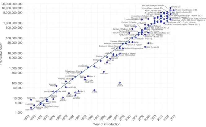
Since 1965, Moore's law has charted the advancement of semiconductor integrated circuits. The scaling of silicon transistor dimensions into the nanometer size drives the exponential increase in the density and performance of complementary metal-oxide-semiconductor (CMOS) technology. For more than fifty years, the microelectronic industry has followed extremely successfully the motto ‘smaller is better’. The transistor count of integrated circuit chips doubles approximately every two years, and the improvement in switching energy, switching speed and cost per transistor improves exponentially as MOSFETs have decreased in size [1]–[4]. Fig. 1-1 depicts such geometric growth of transistor count in the past fifty years [5].
However, it has been predicted that conventional transistor scaling would slow down significantly and eventually end around 2025 [6], [7], when the physical limits of silicon-based metal-oxide-semiconductor field-effect transistors (MOSFETs) would be reached [8]. In fact, as early as 2005, it has been argued by Gordon Moore himself that Moore’s law would end by then because of the exponential nature of the growth. In recent years, there have been increasing expressions of concern and arguments on whether Moore’s law will die soon. Nevertheless, facing unprecedented
24
challenges, researchers worldwide have been pushed to be evermore creative. Extraordinary innovations have been made in CMOS research in recent years and Moore’s law is still marching forward.
To understand CMOS scaling and the associated challenges, one needs to identify that in logic chips, transistors are used as switches, and the goal is to switch between the ON state and OFF state with maximum speed but minimum energy. The switching delay of a MOSFET is approximately:
𝜏𝑑~𝐶𝐺𝑉𝐷𝐷
𝐼𝑂𝑁 (1-1)
Fig. 1-1: Transistor count in integrated processors from 1971-2016, illustrating Moore’s Law. Figure adapted from [5].
25 And the switching energy is approximately:
𝐸𝑑~𝐶𝐺𝑉𝐷𝐷2 (1-2)
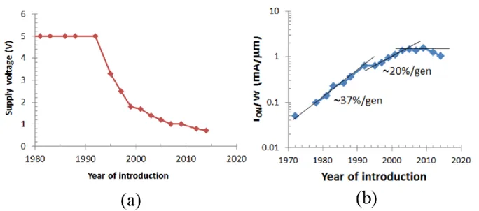
τd, the delay time, is proportional to CG, the total gate capacitance, and VDD, the supply voltage,
and inversely proportional to ION, the ON-state current. Fig. 1-2 illustrates the historic scaling
behavior of VDD and ON-state current density (ION/W) [9]. In the early years of CMOS scaling,
VDD remained constant and ION increased at a rate of roughly 37% per generation, which can be
referred to as a constant-voltage scaling path. Beyond 2000, the electric field in the transistor became intolerable so that VDD (along with threshold voltage VT) had to decrease This heralded
the era of constant-field scaling. As a result, the increase in current density slowed down to ~20% per generation and eventually reached a plateau (and is even dropping more lately). As VDD
continues to drop, obtaining increased performance becomes harder and harder.
Fig. 1-2: (a) Supply voltage scaling of CMOS technologies. (b) ON-state current density scaling for n-channel Si MOSFETs at nominal operation voltage.
26
The above discussion is a simplistic view of CMOS scaling, and a comprehensive and insightful study of the scaling properties can be found in [9]. Currently, MOSFET scaling can be best described as power-constrained scaling, as the dynamic power density has become as high as 100 W/cm2 [10]. Further transistor scaling requires more reduction in V
DD and hence greater
compromises in device performance. In addition, as the channel length of Si MOSFETs has entered the nanometer-scale, short-channel effects have become severe, undermining the scaling benefits. Therefore, future CMOS technology requires innovations in both materials and device structures.
1.2 Multi-gate MOSFETs
As discussed earlier, the driving force behind transistor evolution is the scalability of Si CMOS. Footprint scaling demands all device dimensions to shrink together while delivering maximum performance at reduced voltage. This is a strict demand as device dimensions shrink into the sub-micron regime, where short-channel effects (SCEs) in MOSFETs become severe and catastrophic. SCEs, include mobility degradation, drain-induced barrier lowering (DIBL), degradation of subthreshold swing, leakage, and device variability. To resolve the serious challenges of planar CMOS, which cannot maintain acceptable SCEs at deeply-scaled technology nodes anymore, innovations in device structure need to be made. The evolution of device structures can be depicted in Fig. 1-3. To mitigate SCEs, extremely-thin-body-silicon-on-insulator (ET-SOI) MOSFET and multi-gate transistor structures have been proposed to enhance the electrostatic control of the gate to the channel. In ET-SOI, the channel is made sufficiently thin so that it is fully depleted. In multi-gate transistors, the channel is under control of more than one multi-gate. For example, in a FinFET (double-gate MOSFET), the fin channel is fully depleted when it is narrow enough, so that the
27
entire channel is controlled by the gates on both sides. These non-planar MOSFET designs in effect shorten the characteristic electrostatic length of the device:
𝜆𝑛𝑜𝑛−𝑝𝑙𝑎𝑛𝑎𝑟 = √𝜖𝑠 𝜖𝑜𝑥𝑥𝑜𝑥 𝑥𝑆𝑖 𝑛 = 𝜆𝑝𝑙𝑎𝑛𝑎𝑟√ 𝑥𝑆𝑖 𝑛 ⋅ 𝑥𝑑 (1-3)
where εs and εox are the electron permittivity of channel and gate oxide, xSi and xox is the width or
thickness of the channel and gate oxide, xd is depletion width of the ideal planar MOSFET, and n
is the gate number. The gate number is 1 for ET-SOI, 2 for FinFETs, 3 for Tri-gate MOSFETs, and 4 for gate-all-around (GAA) MOSFETs, respectively. Therefore, alternative designs can reduce the characteristic electrostatic length, λplanar, and in other words, mitigate short-channel
effects.
The multi-gate designs bring more complexity to device fabrication, as the channel is no longer planar but three-dimensional. However, much progress has been made in research and industry Fig. 1-3: Evolution of MOSFET structural designs with increasing electrostatic gate control of the channel from left to right, reproduced from [14].
28
along this path, and tri-gate MOSFETs have already been the mainstream of today’s logic transistors. It is believed that futures innovations in device technology will enable more advanced device structures, such as GAA nanowire MOSFETs and even vertical nanowire (VNW) MOSFETs.
1.3 Advantages of III-V channel MOSFETs
The other possible solution to maintaining or even improving transistor performance while continuing to reduce the supply voltage is to introduce alternative channel materials. In recent years, much research has been made on several novel materials, such as 2-D materials (graphene, MoS2) [11], carbon nanotubes [12], germanium [13], gallium-nitride, and III-V compound
semiconductors [1], [14]. In this regard, III-V compound semiconductors have been regarded as one of the most attractive and feasible candidates to replace Si [1]. III-V compound semiconductors, especially the arsenide-based (InxGa1-xAs) and antimonide-based (InxGa1-xSb)
compounds, are known for their superior electron and hole transport properties over silicon. III-V compound semiconductors are advantageous over other candidates, because the fabrication process of III-V transistors is mostly compatible with present Si CMOS process. Moreover, GaAs and InP are the most advanced in terms of large wafer manufacturing, which can be achieved on wafer-scale substrates. Therefore, in the last few years, increasing research efforts have been devoted to the development of III-V nanometer-scale logic transistors.
29
For modern deeply-scaled MOSFETs, according to the virtual source model [4], [15], ION can be
described as:
𝐼𝑂𝑁 = 𝑣𝑖𝑛𝑗⋅ 𝑄𝑖𝑛𝑗≅ 𝑣𝑖𝑛𝑗⋅ 𝐶𝑖𝑛𝑗⋅ (𝑉𝐷𝐷− 𝑉𝑇) (4)
, where vinj is the source injection velocity, Qinj is the charge density at the virtual source, and (VDD
– VT) is the gate overdrive. Fig. 1-4 illustrates the injection velocity extracted from Si and strained
Si MOSFETs at VDS of 1.1-1.3 V, along with the injection velocity of InGaAs and InAs high
electron mobility transistors (HEMTs) at VDS = 0.5 V, as a function of gate length. For Si
Fig. 1-4: Electron injection velocity in Si and strained-Si MOSFETs, InGaAs and InAs HEMTs with different channel compositions, as a function of gate length. Figure reproduced from [1].
30
MOSFETs, vinj maximizes at 1∙107 cm/s, and reaches nearly 1.5∙107 cm/s for strained Si. For
InGaAs and InAs at less than half the operating voltage, vinj can be more than twice or three-times
that of Si MOSFETs. This is attributed to the lower electron effective masses of InxGa1-xAs. In
the ballistic limit, the injection velocity is closely related to the carrier mobility as 𝑣𝑖𝑛𝑗~𝜇𝛼, where
α ≤ 0.5 [4]. Therefore, to the first order, III-V channels with a higher mobility promise to provide higher vinj in short channel devices. Fig. 1-5 shows the evolution of transconductance, gm, of Intel’s
Si MOSFETs and InGaAs MOSFETs, as a function of year of demonstration. In recent years, rapid progress has been made in InGaAs MOSFETs, demonstrating a maximum gm of 3.45 mS/μm, with
Lg = 70 nm and VDS = 0.5 V [16], [17], exceeding that Si’s 32 nm node, which is the last node
Fig. 1-5: Transconductance of Intel’s Si MOSFETs and InGaAs MOSFETs vs. year of demonstration.
31
before Intel introduced 3-D Tri-gate transistors. This progress shows that III-V MOSFETs have great potential for future logic and high-speed circuits even at lower operating voltage.
1.4 P-Channel MOSFETs
CMOS technology requires high performance from both NMOS and PMOS transistors. Because of the lower carrier mobility of holes, much research efforts in p-type MOSFETs are needed in order to match the performance of n-type MOSFETs. In unstrained Si, the current density of the PMOS transistor has been about one-third that of the NMOS transistor, and circuit designers learned to work with this imbalance. On the other hand, because of the development of strain engineering, the Si PMOS has been able to catch up with the performance of the NMOS. In state-of-the-art Si CMOS with 7th-generation strained Si, ION of PMOS transistors has improved to ~80%
of that of NMOS transistors [18]. Uniaxial compressive stress is usually obtained by creating stressed regions in the source and drain sides using SiGe, which has a larger lattice constant than Si. The compressive strain to the Si channel changes its lattice constant and therefore the band structure, and it can result in a significant enhancement in the hole mobility. In fact, over several generations of strained Si CMOS technologies, the hole concentration of Ge in the source and drain has kept increasing, and the source/drain/gate spacing has kept decreasing, resulting in increased stress [19]–[22].
32
For alternative p-type MOSFETs, Ge has the highest bulk hole mobility among conventional semiconductors and it looks very promising for its maturity in Si CMOS technology. SiGe regrowth and strain engineering has already been applied in the standard CMOS fabrication process. Current state-of-the-art high-Ge-content strained SiGe p-channel FinFETs have shown record gm as high as 2.7 mS/μm, by aggressive Lg and EOT scaling (Lg ~ 25 nm, EOT ~ 0.7 nm)
[23]. On the other hand, Ge NMOS transistors have not been able to demonstrate performance as
Fig. 1-6: Electron (red) and hole (blue) mobility of III-V compound semiconductors in reported devices, plotted against the lattice constant. The arrows represent the impact of biaxial strain on mobility. The hole mobility of InGaSb can be almost doubled under application of compressive strain.
33
good as InGaAs/InAs NMOS transistors. Therefore, future technology integrating InGaAs as NMOS channel and Ge as PMOS will pose challenges to the manufacture process [24].
Another option for alternative-channel CMOS is the III-V CMOS technology. Fig. 1-6 plots the highest room-temperature electron and hole mobilities of the III-V family, together with Si and Ge, reported in inversion layers and quantum wells, as a function of the corresponding lattice constant [1]. The impact of increasing compressive biaxial stress is indicated by the arrows. For electron transport, the InxGa1-xAs system and InSb shows the highest electron mobility.
Unfortunately, InxGa1-xSb n-channel MOSFETs have never been demonstrated, though the
electron mobility is predicted to be quite high. For hole transport, the InxGa1-xSb family shows the
highest hole mobility, and it is the only III-V compound which can match the hole mobility of pure Ge. In addition, the hole mobility of InxGa1-xSb can be increased effectively by strain [25], bridging
the gap between the electron mobility of other III-Vs. A hole mobility as high as 1,500 cm2/V∙s
has been reported in strained In0.4Ga0.6Sb [26], 1,300 cm2/V∙s in GaSb [27], and 1,200 cm2/V∙s in
InSb [28].
While the carrier transport properties favor the III-V compound semiconductors, transistor technology must be developed and high-performance devices need to be delivered to advance the III-V technology in real-world applications. Recently, rapid progress has taken place in the development of InGaAs-based n-channel MOSFETs. From HEMTs [29], [30] to planar MOSFETs [31] to FinFETs [32] and to nanowire gate-all-around MOSFETs [33], [34], we have witnessed a surge of device innovations and demonstrations in the InGaAs system.
34
Besides the InGaAs system, antimonides, particularly InxGa1-xSb, are attractive materials due to
their extraordinary hole mobility, as well as their decently high electron mobility, as highlighted in Fig. 1-6. In addition, the antimonide family has lattice constants around 6.1 Å. Therefore, a fully III-V-on-Si CMOS integration scheme is possible by integrating InGaAs NMOS and InGaSb PMOS, or InGaSb for both NMOS and PMOS, as shown in Fig. 1-7. Several preliminary work has demonstrated such III-V CMOS integration [35]–[37]. Moreover, the antimonide family owns a wide range of band gap energies. Therefore, band gap engineering can be exploited using the antimonides without excessive lattice mismatch. For example, antimonides have been found essential in building InAs/GaSb tunnel FETs (TFETs) [38]–[40], which is a very promising class of novel devices for ultra-low power applications.
Fig. 1-7: Possible III-V-on-Si integration scheme using intrinsic InGaSb single channel for future CMOS technology with alternative channel materials.
35
However, the progress in the antimonide-based transistors, until recently, became stagnant. Although a few demonstrations of InGaSb p-channel transistors have been demonstrated [35], [37], [41]–[48], the device performance has been unsatisfactory. Fig. 1-8 shows two works that have had great influence on antimonide device research. Since around 2000, B. R. Bennett et al. have demonstrated InAs/AlSb p-channel HEMTs and have developed the key technology of molecular beam epitaxy growth of antimonides [45], [49]. In 2010, A. Nainani et al. have demonstrated the first InGaSb buried-channel pMOSFET that outperforms Ge with two times higher hole mobility [44], [50]. Nevertheless, the gap between antimonide device research with Ge or InGaAs devices remains large. Fig. 1-9 shows the number of publications on InGaAs transistors in IEEE journals alone vs. the number of Sb-based devices in all literature to date. This comparison not only shows the large discrepancy in the research effort, but also implies the tremendous challenges in antimonide device research. In fact, antimonide-based multi-gate MOSFETs have never been demonstrated before this thesis work.
Fig. 1-8: Cross-section of (left) InAs/AlSb p-channel HEMT [45] and (right) InGaSb buried-channel pMOSFET [44].
36
The lack of InGaSb multi-gate MOSFETs can be attributed to several challenges. First, antimonide-based fin or nanowire etching has never been successfully demonstrated. All existing approaches to form 3-D antimonide structures rely on epitaxial growth, which is not CMOS-compatible. Second, antimonide compounds are highly reactive and unstable. When exposed to air, a layer of native oxide is instantly formed. What is even worse, the oxidation of InGaSb is not self-limiting, and the formed oxide layer severely degrades the device performance because of Fermi-level pinning. In addition, antimonides are easily attacked by most acids and bases used commonly in CMOS fabrication, such as hydrofluoric acid and sulfuric acid, which are common etchants, and tetramethylammonium hydroxide (TMAH), which is widely present in photolithography developer. Therefore, cleaning and passivation of the Sb surface are difficult, and formation of a quality interface with the k gate dielectric is challenging. Third, high-quality nano-scale ohmic contacts for antimonide-based devices have not been thoroughly
Fig. 1-9: Count of publications of InGaAs transistors in IEEE journals alone vs. the count of Sb-based devices in all literature to date.
37
investigated. As device footprints scales, source-drain contact resistance plays an important role by limiting the drive current. Eventually, and most critically, a 3-D process integration of a FinFET is a significantly more complex fabrication task than that of a planar transistor, even after resolving the challenges enunciated above. Therefore, it is the goal of this thesis work to overcome the above challenges and demonstrate the first InGaSb p-channel FinFET.
1.5 Thesis Overview
This thesis studies some novel solutions to the formerly described challenges with InGaSb p-channel multi-gate transistor technology. Since no such device has ever been demonstrated, this thesis aims to start from the fundamental technological challenges of antimonide-based process, then move on to the demonstration of full transistor fabrication, and eventually investigate the electrical performance of the InGaSb multi-gate transistors.
In the first part of the thesis, the goal of demonstrating the first InGaSb multi-gate transistor is tackled in a divide-and-conquer approach. Prior to a complete device design and fabrication, solutions to the challenges mentioned above need to be delivered. Three main technologies are developed. First, an antimonide reactive ion etching (RIE) technology is developed. The RIE technology can etch antimonide fins and vertical nanowires with high aspect ratio, anisotropy, and sidewall smoothness. The new technology is also compatible with other III-V compounds, such as arsenides. Second, a novel alcohol-based digital etch technology is invented. It can be used to perform fin and nanowire sidewall etching with nanometer precision, at a rate of 2.0 nm/cycle. It also serves as a surface passivation method for the high-k dielectric/InGaSb interface. It has been
38
found to improve interfacial quality and reduce leakage current. Last, a nanoscale ohmic contact scheme using nickelide is developed and analyzed. It achieves record ultra-low contact resistance. A composite p+ capping layer is designed to reduce the contact resistance.
In the second part of the thesis, the above technologies are applied and integrated into the design of an InGaSb p-channel FinFET. The design principles of the heterostructure and process of the proposed device are explained. Then, a fabrication process is developed for the actual transistors. The smallest devices achieved feature a minimum fin width of 10 nm and a gate length of 20 nm. It is the not only the first demonstration of InGaSb FinFET, but also one of the most aggressively scaled devices based on III-V compound semiconductors. Lastly, the electrical characteristics of three generation of fabricated InGaSb FinFETs are reported and analyzed.
39
CHAPTER 2. PROCESS DEVELOPMENT
2.1 Process Overview
Following the introduction in Ch. 1, this chapter describes the key processes required in a self-aligned InGaSb p-channel FinFETs. As described in the previous chapter, various critical fabrication technologies for antimonide-based multi-gate transistors are not yet available. To achieve the goal of demonstrating the first InGaSb FinFET, this part of the thesis focuses on an effort to develop three major components of an antimonide-based FinFET. Those are (1) fin reactive ion etching, (2) ohmic contact, and (3) digital etch. All the three components are supposed to be optimized for the antimonides, and even better, compatible to the arsenides.
2.2 Fin Reactive Ion Etching
2.2.1 Antimonide RIE – First Generation
As its name suggests, fin etching is the essential process module for the FinFET fabrication. In our top-down approach, the reactive ion etching (RIE) is required to deliver high-aspect ratio fins with nanometer-scale fin width. In addition, the RIE process needs to be both anisotropic and gentle so that the profile of the fin is vertical and uniform while the sidewall of the fin remains smooth.
40
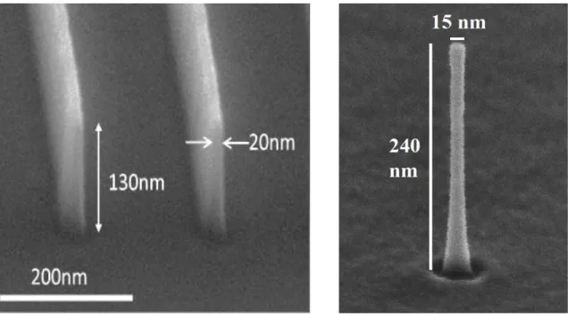
In recent years, there have been tremendous breakthroughs in the InGaAs FinFET and vertical nanowire (VNW) MOSFET technologies [32], [34], [51]–[54]. The InGaAs fin RIE process is the backbone of these high-performance transistors. Fig. 2-1 shows some examples of the state-of-the-art InGaAs fin and VNW etching developed in our group [34], [55].
An example of the starting antimonide-based heterostructure used in this thesis is shown in Fig. 2-2. It is grown by molecular-beam epitaxy. The details of the design and properties of the heterostructure will be described in Ch.3 when the FinFET process integration is discussed. Note that a typical etched fin structure contains multiple compounds, such as InGaSb, AlGaSb, and
Fig. 2-1: (left) InGaAs fins with 20 nm fin width and (right) InGaAs VNW with 15 nm diameter, patterned by optimized RIE process.
41
perhaps InAs, with different compound compositions. Therefore, the RIE process needs to show ideally negligible material selectivity for various III-V compounds semiconductors.
The first step to form the fins is the patterning of etching hardmask. In this thesis, HSQ1 (hydrogen
silsesquioxane), a flowable oxide diluted with methyl-isobutyl-ketone (MIBK), is used as the hardmask and patterned by electron beam lithography (EBL). Before HSQ spin coating, the wafer surface is coated with a thin Si3N4 film deposited by plasma-enhanced chemical vapor deposition
(PECVD) at 300 °C to promote adhesion of HSQ on the semiconductor surface. The thickness of the PECVD Si3N4 film is only 2-3 nm to avoid complication of the fin etching process. Then, the
1 HSQ is distributed by Dow Corning as XR-1541TM.
42
HSQ is spin coated onto the sample and exposed in the Elionix ELS-F125 EBL system, with a resolution of 5 nm at a beam current of 1 nA. After the e-beam exposure, the HSQ is immediately developed in 25% tetramethylammonium hydroxide (TMAH) for 60s, followed by DI water and isopropanol rinsing, and blown dry gently by N2 gun. It has been suggested that development of
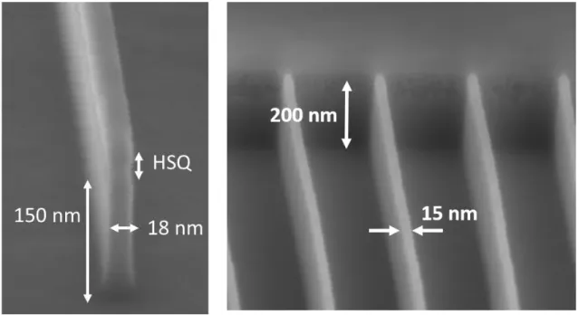
HSQ in low temperature in cold-water bath improve the resist contrast for high-resolution patterns [ref]. From our experience, room temperature development suffices for patterns as small as 15 nm. On the other hand, it is worth noting that both the exposure and development of HSQ are done in the same day to avoid HSQ crosslinking in air, in order to ensure best optimal resolution and reproducibility. Fig. 2-3 shows scanning electron microscopy (SEM) images of developed HSQ nanowire pattern with 26 nm diameter and fin patterns with various widths.
Then, the RIE is carried out in an inductive coupled plasma (ICP) etcher SAMCO RIE-200iP, using chlorine-based etching. Samples were cleaved into approximately 1x1 cm2 small rectangular
pieces and loaded on a 6-inch ceramic wafer carrier, one sample at a time. In the case of very small Fig. 2-3: Tilted SEM images of developed HSQ (left) nanowire pattern with dimeter of 26 nm and (right) fin patterns with different width.
43
sample size (e.g. for testing or calibration purpose), a 1x1 cm2 GaAs wafer is put next to the sample
to avoid variability caused by loading effect.
After iterative tuning of the gas chemistry, gas flow, and etching power, the etching condition is optimized to the following condition: 13.5/5.5 sccm BCl3/N2, 20 W ICP power, 280 W RF platen
power, 0.2 Pa chamber pressure, and substrate temperature of 250°C. The etched fins are shown in Fig. 2-4. This is the first demonstration of RIE of antimonide-based fins. Both single fins and arrays of fins with vertical profile and smooth surface can be obtained. The resulted fins have high aspect ratio > 10 and no noticeable undercutting or trenching is observed.
Fig. 2-4: SEM images of (left) single InGaSb fin with 18 nm fin width and 150 nm fin height, and (right) fin array with 15 nm fin width and 200 nm fin height.
44
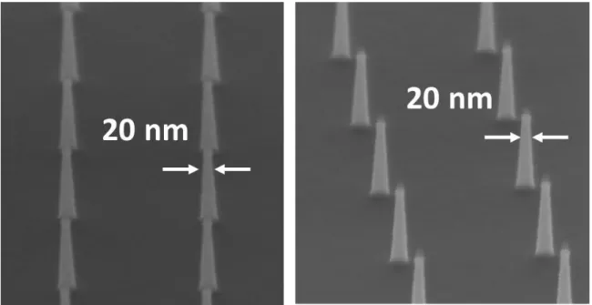
The developed RIE process is also able to etch InGaSb vertical nanowires with high aspect ratio and vertical profile (> 85). Moreover, dense fin arrays can be achieved, with 20 nm fin width and 20 nm fin spacing, which is equivalent to a full pitch size of 40 nm. Examples of an InGaSb VNW and tight-pitch fin array is demonstrated in Fig. 2-5.
Fig. 2-5: SEM images of 20 nm InGaSb vertical nanowire and dense fin array with 20 nm fin spacing.
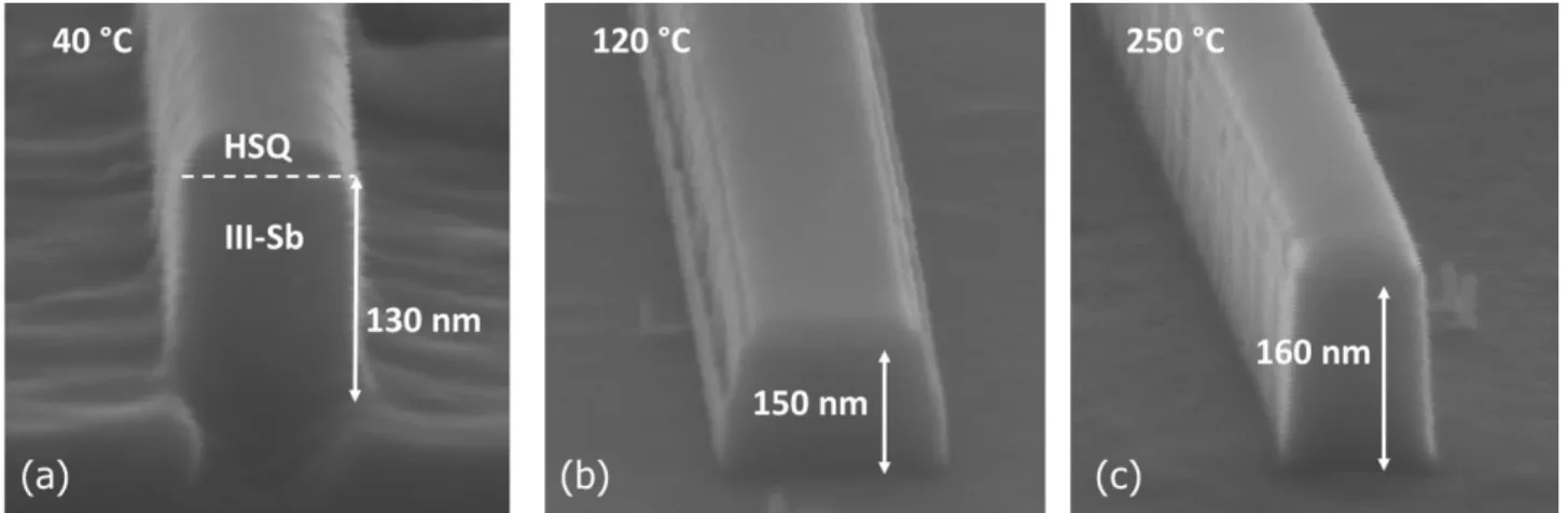
Fig. 2-6: RIE of antimonide-based heterostructures using HSQ hardmask at: (a) 40C, (b) 120C, and (c) 250C substrate temperature during etching.
45
The dry etching of antimonide fins shows strong dependence on the substrate temperature. Fig. 2-6 shows the same etched fin test structures at different substrate temperatures of 40C, 120C and 250C, with other etching conditions unchanged. It illustrates the clear benefit of higher substrate temperature during the RIE. Raised substrate temperature increases the etch rate from 65 nm/min at 40C to 80 nm/min at 250C. At higher substrate temperature, the resulted fin sidewall and surface are smoother and profile is more vertical. Raised temperature etching is necessary because of the lower volatility of InClx. In this thesis, the etching temperature is kept at 250C because it
is the highest temperature the heater allowed in our etcher system. Nevertheless, the results are already indeed very promising. Fig. 2-7 shows that the etched fin sidewall appears to be very smooth with little material selectivity.
46 2.2.2 Antimonide RIE – Second Generation
The RIE process described above has been integrated into the first and second generation of InGaSb FinFET fabrication. In the third generation of FinFETs, an improvement has been made to the RIE technology so that it is compatible to arsenide-based compound semiconductors. The RIE is performed by ICP plasma with the following condition: 3:11:0.4 sccm BCl3/Ar/SiCl4, 280
W RF platen power and 20 W ICP power, at 250 C. Fig. 2-8 shows fins comprising of 50 nm InAs on GaSb with the former mentioned RIE process and the improved one. With the former RIE condition, the InAs layer is roughened during dry etch, while a smooth sidewall is obtained with the improved RIE condition. Therefore, simultaneous etching of antimonides and arsenides is achieved without roughening any of the surface. This is significant when dry etching of both types of III-V compounds is required, for example, for InAs/GaSb tunnel FETs (TFETs). This etching condition is deployed in the third generation of the InGaSb FinFETs.
Fig. 2-8: SEM images of RIE-etched InAs/GaSb fins using the RIE condition of (left) 13.5/5.5 sccm BCl3/N2, and (right) 3:11:0.4 sccm BCl3/Ar/SiCl4. In both cases, RF platen power is 280
47
It is worthy to note here that high-quality fin RIE is necessary but not sufficient for highly scaled high performance III-V FinFETs. First, the fin width is limited by the capability and resolution of the electron-beam lithography, which is limited to around 15 nm and beyond. Second, considerable plasma damage might be taking place, especially when anisotropic etching is desired and therefore the plasma power is large. Surface cleaning technique for etched fin sidewalls is particularly important for antimonides because of their highly reactive and unstable surface. Therefore, a digital etch technology is in dire need to scale the device further down and improve the surface quality. In the following chapter, I will describe the development of the digital etch technology for antimonides.
2.3 Digital Etch
One issue of top-down approach of FinFET fabrication via dry etching is the RIE damage of the fin sidewall, due to the high energy ion bombardment during the etch [56]–[59]. The quality of the fin sidewall is one of the most critical factors for FinFETs operation, because the current flows in close proximity to the surface. In Si FinFETs fabrication, high temperature forming gas annealing at above 850°C has been shown to be an effective approach to improve the surface quality [60]. However, processing at such high temperature is unfeasible for III-V transistors. Although direct wet etching can be used to remove RIE-damaged semiconductor, it is not applicable to deeply scaled devices, which require nanometer-scale etching precision.
48
In silicon CMOS technology, the concept of digital etch (DE) or atomic layer etching (ALE) has been proposed and developed for more than twenty years [61], [62]. In such process, layer-by-layer etching of Si can be achieved at atomic scale, by a repeated process of surface modification and surface removal reactions that are self-limiting. For example, the surface modification step can be fluorination of the Si surface by CF/O2 plasma to form a thin layer of volatile silicon
fluoride. Then, the surface removal step can be achieved by Ar+ ion irradiation. As the
semiconductor industry has entered the era of atomic-scale dimensions, the digital etch technology is turning to be increasingly critical and is under active research. Inspired by the Si digital etch and atomic layer etching technology, the similar concept has been introduced to III-V compound semiconductor as well, as an effective to modify the surface property at atomic-layer scale.
2.3.1 III-V Digital Etch
In the quest for enhanced performance over silicon devices at advanced nodes, III-V multi-gate transistors such as FinFETs or nanowire gate-all-around MOSFETs are being pursued with fin width or nanowire diameter in the sub-10 nm range. In this dimensional regime, precise etching control is paramount. Inspired by the atomic layer etching technology developed in silicon [61], [62], the concept of digital etch was introduced to III-V compound semiconductors [63]–[68]. In digital etch, the oxidation and oxide removal steps characteristic of chemical etching are performed separately. This makes them both self-limiting affording nanometer-scale control of the etching process. Digital etch has been shown to preserve high aspect ratio features, enabling precise device dimension engineering. It has also been shown to be effective in mitigating surface damage induced by RIE [69]. In the last few years, the use of digital etch has enabled demonstrations of
49
aggressively scaled III-V FinFETs and NW-MOSFETs with exciting electrical characteristics [38], [39], [70]–[72].
Prior to this thesis work, digital etch has been solely applied to arsenide-based III-Vs, achieving a smallest feature size of 5 nm in fins [55] and 7 nm in lateral nanowires [38]. On the other hand, demonstrations of high aspect ratio vertical nanowires (VNW) by digital etch have been limited to 11-15 nm in diameter [39]. Firstly, conventional digital does not work on antimonide-based III-Vs, because antimonides are typically highly reactive, and therefore a benign and stable self-limiting digital etch process is challenging. Secondly, a digital etch process for fins and VNWs with critical dimensions approaching sub-10 nm regime is desired to push the state-of-the-art of III-V transistor technology, regardless in InGaAs or InGaSb.
Fig. 2-9 illustrates the typical process flow of a digital etch process. After the fin RIE, the surface is oxidized using oxygen plasma (in an asher), at 1 kW for 3 minutes. Other oxidation agents include hydrogen peroxide, ozone, or ozonated water. Then, the oxidized surface is etched away by some acid solutions, such as hydrochloric acid or sulfuric acid, which are supposed to have
50
negligible etching rate on the III-V. Afterwards, the same procedure of oxidation and oxide removal is repeated in cycles, removing one layer at a time.
Fig. 2-10, adopted from [67] shows the digital etch rate per cycle on planar InP wafer, as a function of oxygen exposure time, fitted by the Lukeš’ rate law [73]. It shows saturation behavior beyond 180 seconds of oxidation time, illustrating the self-limiting property of the oxidation process. Fig. 2-11 illustrates the progress of digital etch process on an InGaAs vertical nanowire in a sequential etch experiment after 2, 5 and 10 cycles of digital etch using oxygen plasma and 10% HCl. The initial diameter of the VNW after RIE is 34 nm, and after 10 cycles, the diameter is reduced to 14 nm. The average etch rate is 1 nm/cycle, on each side of the VNW. It can be observed that the Fig. 2-10: Etch rate per cycle of digital etch on InP planar wafer, as a function of oxidation time under O2 plasma, adapted from [66], fitted with the Lukeš model [73].
51
digital etch preserves well the profile of the VNW. It proves the unpreceded benefit of using digital etch to achieve nanometer-scale scaling of device dimensions.
Another important benefit of digital etch is its ability to mitigate plasma damage and improve surface quality. By removing the semiconductor surface layer by layer, the surface roughness is improved and better device performance can be obtained. Fig. 2-12 shows the subthreshold characteristics of InGaAs VNW MOSFETs with and without digital etch (10 cycles), with the transconductance (gm) characteristics in the inset [69]. While the two transistors are almost
identical (Dfinal = 30 nm), the transistor with digital etch shows lower subthreshold swing of 150
mV/dec (at Vds = 50 mV), and higher peak gm of 280 μS/μm (at Vds = 0.5 V). These results show
the significant reduction of sidewall damage by the digital etch process.
Fig. 2-11: Evolution of InGaAs VNWs in a sequential etch experiment involving different numbers of digital etch cycles in 10% HCl:IPA.
52
Because of the above benefits, digital etch has been widely applied in recent InGaAs MOSFET fabrication. However, there is yet no digital etch reported in the antimonide-based material system. In fact, there is no prior study on surface treatment of antimonide fin/VNW sidewall. Because of the development of our InGaSb fin RIE technology, we are able to study this topic for the first time.
2.3.2 Antimonide-compatible Digital Etch
In principal, both the oxidation and oxide removal steps of digital etch need to be self-limiting. Unfortunately, neither of the two self-limiting steps can be easily obtained in the antimonide-based devices. First, antimonide-based compounds are notoriously known for its highly reactive surface.
Fig. 2-12: Subthreshold and transconductance (inset) characteristics of InGaAs VNW MOSFETs, with final diameter of 30 nm, with and without digital etch [69].
53
The oxidation of GaSb is very fast even in air, and in theory non-limiting [74]. Second, the etching or removal of native oxide of antimonides is difficult. Chemical cleaning of GaSb surface has been studied for many years [74]–[80], and there is no demonstration of effective approaches. Most popular methods is using diluted HCl:H2O solution, which has been shown to remove GaOx and
SbOx from the surface [75]. In addition, all existing studies on antimonide surface cleaning or
passivation were carried out on planar wafers, and the impact is characterized by surface studies such as x-ray photoelectron spectroscopy (XPS), or electrically by capacitance-voltage (C-V) measurement. There is little information about the etch rate and selectivity, particularly in the case of vertical structures or sidewalls.
Fig. 2-13 shows tilted SEM images demonstrating the effect of a 30 second dipping of InGaSb VNW in 1% diluted HCl:H2O solution. It is observed that the diameter of the VNW decreased
from 116 nm to 106 nm. Also, the shape of the VNW is changed, and the surface of the sidewall Fig. 2.-13: Etched InGaSb/AlGaSb VNWs with initial diameter of 116 nm (left), after 30s dipping in 1% HCl:H2O (middle). (Right) schematic showing the effect of HCl cleaning on
54
becomes rougher. This shows that HCl:H2O treatment is not self-limiting and is etching the InGaSb
and AlGaSb at different rates. This poses the first major challenge of developing digital etch for the antimonides.
After trying several other etchants, it seems that simply replacing the HCl does not solve the problem. Another aspect of the etching process is the solvent of the etchant, which is usually neglected. Fig. 2-14 shows InGaSb nanowire and fin test structures before and after a two-minute dipping in DI water. The diameter of the antimonide nanowire decreases from 100 nm to 92 nm.
Fig. 2-14: Antimonide vertical nanowire (a) before and (b) after dipping in DI water for 2 minutes. (c) Antimonide fin test structure after dipping in DI water for 2 minutes.
55
Also, the nanowire sidewall and AlGaSb field surface become rough and notches appear at the heterojunction interfaces. The antimonide fin sidewall in Fig. 2-14(c) also reveals such etching effect. This etching of antimonide-based heterostructures in water has not been reported prior to this work. It implies that the surface of the antimonides is chemically highly reactive and unstable, so that it can react even in water. Also, the notches formed near the interfaces of heterostructure layers imply preferential etching, possibly due to defects from the epitaxial growth and strain, as antimonide-based heterostructures are generally not lattice matched.
Therefore, to develop the digital etch, water needs to be removed first from the process. Fig. 2-15 shows VNWs with the same antimonide heterostructure, before and after 2 minutes dipping in 10% HCl:IPA2. By using an alcohol-based solution, no noticeable sidewall etching or surface
2 The solvent-based acids are commercially available at Sigma-Aldrich Co as HCl-2-proponol solution.
Fig. 2.15: Antimonide vertical nanowires with 20 nm diameter (left) before and (right) after dipping in 10% HCl:IPA for 2 minutes.
56
damage is observed, implying that the etching is self-limiting after removing the layer of oxide on the sidewall.
With the discovery of the alcohol-based treatment, digital etch on antimonide-based heterostructure is demonstrated for the first time. Oxidation is done by O2 plasma as described
above. Fig. 2-16(a) shows the radial etch rate of digital etch on InGaSb vertical nanowires as a function of number of digital etch cycles. Fig. 2-16(b) shows an InGaSb fin obtained after 5 cycles of digital etch in HCl:IPA, with a minimum fin width of 10 nm.
Fig. 2-16(a) reveals an additional issue that remains with antimonide-based digital etch. For the first two cycles of digital etch, the radial etch rate is 2 nm/cycle, while the etch rate decreases to an average only 0.6 nm/cycle for the next 4 cycles. This is inconsistent with how digital etch works Fig. 2-16: (a) Evolution of antimonide VNW diameter with number of digital etch cycles in 10% HCl:IPA. (b) 10 nm wide InGaSb fin obtained after 5 cycles of digital etch in HCl:IPA.
57
with InGaAs, in which the etch rate is independent of the numbers of cycles. Therefore, it is possible that the surface property of the antimonide is changed after the treatment of digital etch.
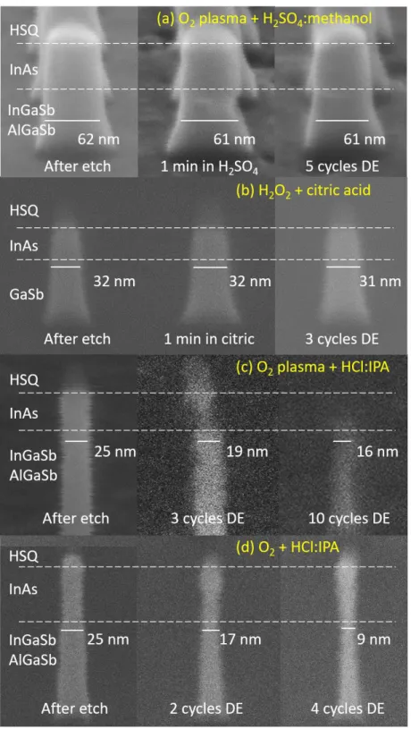
Fig. 2-17 shows sequential digital etch of antimonide-based vertical nanowire in O2 plasma and
HCl:IPA. The nanowire contains InAs, as well, so that the digital etch on the two compounds can be monitored together. Alcohol-based digital etch produces an initial radial etch rate on the III-Sb of 1.0 nm/cycle, while the etch rate on the InAs portion of the nanowire is about 2.0 nm/cycle. It is an important deficiency that the digital etch has material selectivity. In addition, after 10 cycles, the average etch rate on the III-Sb portion of the structure is drastically reduced to about 0.21 nm/cycle, while all the InAs has already been etched away. Other researchers have reported a similar much reduced etch rate of GaSb in water-based digital etch [40].
Fig. 2.17: (a) InAs/InGaSb/AlGaSb vertical nanowire after RIE with initial diameter of 25 nm, and after (b) 3 cycles and (c) 10 cycles of digital etch in O2 plasma and HCl:IPA. Noted are