Publisher’s version / Version de l'éditeur:
Vous avez des questions? Nous pouvons vous aider. Pour communiquer directement avec un auteur, consultez la première page de la revue dans laquelle son article a été publié afin de trouver ses coordonnées. Si vous n’arrivez pas à les repérer, communiquez avec nous à [email protected].
Questions? Contact the NRC Publications Archive team at
[email protected]. If you wish to email the authors directly, please see the first page of the publication for their contact information.
https://publications-cnrc.canada.ca/fra/droits
L’accès à ce site Web et l’utilisation de son contenu sont assujettis aux conditions présentées dans le site LISEZ CES CONDITIONS ATTENTIVEMENT AVANT D’UTILISER CE SITE WEB.
ACS Nano, 14, 1, pp. 28-117, 2019-09-03
READ THESE TERMS AND CONDITIONS CAREFULLY BEFORE USING THIS WEBSITE.
https://nrc-publications.canada.ca/eng/copyright
NRC Publications Archive Record / Notice des Archives des publications du CNRC : https://nrc-publications.canada.ca/eng/view/object/?id=e38fec49-0637-43f8-beb0-09dae6a7621f https://publications-cnrc.canada.ca/fra/voir/objet/?id=e38fec49-0637-43f8-beb0-09dae6a7621f
NRC Publications Archive
Archives des publications du CNRC
This publication could be one of several versions: author’s original, accepted manuscript or the publisher’s version. / La version de cette publication peut être l’une des suivantes : la version prépublication de l’auteur, la version acceptée du manuscrit ou la version de l’éditeur.
For the publisher’s version, please access the DOI link below./ Pour consulter la version de l’éditeur, utilisez le lien DOI ci-dessous.
https://doi.org/10.1021/acsnano.9b04224
Access and use of this website and the material on it are subject to the Terms and Conditions set forth at Present and future of surface-enhanced raman scattering
Langer, Judith; Jimenez de Aberasturi, Dorleta; Aizpurua, Javier; Alvarez-Puebla, Ramon A.; Auguié, Baptiste; Baumberg, Jeremy J.; Bazan, Guillermo C.; Bell, Steven E. J.; Boisen, Anja; Brolo, Alexandre G.; Choo, Jaebum; Cialla-May, Dana; Deckert, Volker; Fabris, Laura; Faulds, Karen; García de Abajo, F. Javier; Goodacre, Royston; Graham, Duncan; Haes, Amanda J.; Haynes, Christy L.; Huck, Christian; Itoh, Tamitake; Käll, Mikael; Kneipp, Janina; Kotov, Nicholas A.; Kuang, Hua; Le Ru, Eric C.; Lee, Hiang Kwee; Li, Jian-Feng; Ling, Xing Yi; Maier, Stefan A.; Mayerhöfer, Thomas; Moskovits, Martin;
Murakoshi, Kei; Nam, Jwa-Min; Nie, Shuming; Ozaki, Yukihiro; Pastoriza-Santos, Isabel; Perez-Juste, Jorge; Popp, Juergen; Pucci, Annemarie; Reich, Stephanie; Ren, Bin; Schatz, George C.; Shegai, Timur; Schlücker, Sebastian; Tay, Li-Lin; Thomas, K. George; Tian, Zhong-Qun; Van Duyne, Richard P.; Vo-Dinh, Tuan; Wang, Yue; Willets, Katherine A.; Xu, Chuanlai; Xu, Hongxing; Xu, Yikai; Yamamoto, Yuko S.; Zhao, Bing; Liz-Marzán, Luis M.
Present and Future of Surface-Enhanced
Raman Scattering
Judith Langer,
†Dorleta Jimenez de Aberasturi,
†Javier Aizpurua,
‡Ramon A. Alvarez-Puebla,
§,∥Baptiste Auguié,
⊥,#,7Jeremy J. Baumberg,
8Guillermo C. Bazan,
9Steven E. J. Bell,
10Anja Boisen,
11Alexandre G. Brolo,
12,13Jaebum Choo,
14Dana Cialla-May,
15,16Volker Deckert,
15,16Laura Fabris,
17Karen Faulds,
18F. Javier García de Abajo,
∥,19Royston Goodacre,
20Duncan Graham,
18Amanda J. Haes,
21Christy L. Haynes,
22Christian Huck,
23Tamitake Itoh,
24Mikael Käll,
25Janina Kneipp,
26Nicholas A. Kotov,
27Hua Kuang,
28,29Eric C. Le Ru,
⊥,#,7Hiang Kwee Lee,
30,31Jian-Feng Li,
32Xing Yi Ling,
30Stefan A. Maier,
33Thomas Mayerhöfer,
15,16Martin Moskovits,
34Kei Murakoshi,
35Jwa-Min Nam,
36Shuming Nie,
37Yukihiro Ozaki,
38Isabel Pastoriza-Santos,
39Jorge Perez-Juste,
39Juergen Popp,
15,16Annemarie Pucci,
23Stephanie Reich,
40Bin Ren,
32George C. Schatz,
41Timur Shegai,
25Sebastian Schlücker,
42Li-Lin Tay,
43K. George Thomas,
44Zhong-Qun Tian,
32Richard P. Van Duyne,
41Tuan Vo-Dinh,
45Yue Wang,
46Katherine A. Willets,
47Chuanlai Xu,
28,29Hongxing Xu,
48Yikai Xu,
10Yuko S. Yamamoto,
49Bing Zhao,
50and Luis M. Liz-Marzán
*
,†,51 †CIC biomaGUNE and CIBER-BBN, Paseo de Miramón 182, Donostia-San Sebastián 20014, Spain ‡
Materials Physics Center (CSIC-UPV/EHU), and Donostia International Physics Center, Paseo Manuel de Lardizabal 5, Donostia-San Sebastián 20018, Spain
§
Departamento de Química Física e Inorgánica and EMaS, Universitat Rovira i Virgili, Tarragona 43007, Spain ∥
ICREA-Institució Catalana de Recerca i Estudis Avançats, Passeig Lluís Companys 23, Barcelona 08010, Spain ⊥
School of Chemical and Physical Sciences, Victoria University of Wellington, PO Box 600, Wellington 6140, New Zealand #
The MacDiarmid Institute for Advanced Materials and Nanotechnology, PO Box 600, Wellington 6140, New Zealand 7The Dodd-Walls Centre for Quantum and Photonic Technologies, PO Box 56, Dunedin 9054, New Zealand
8NanoPhotonics Centre, Cavendish Laboratory, University of Cambridge, Cambridge CB3 0HE, United Kingdom
9Department of Materials and Chemistry and Biochemistry, University of California, Santa Barbara, California 93106-9510, United States
10
School of Chemistry and Chemical Engineering, Queen’s University of Belfast, Belfast BT9 5AG, United Kingdom 11
Department of Micro- and Nanotechnology, The Danish National Research Foundation and Villum Foundation’s Center for Intelligent Drug Delivery and Sensing Using Microcontainers and Nanomechanics, Technical University of Denmark, Kongens Lyngby 2800, Denmark
12
Department of Chemistry, University of Victoria, P.O. Box 3065, Victoria, BC V8W 3 V6, Canada 13
Center for Advanced Materials and Related Technologies, University of Victoria, Victoria, BC V8W 2Y2, Canada 14
Department of Chemistry, Chung-Ang University, Seoul 06974, South Korea 15
Leibniz Institute of Photonic Technology Jena - Member of the research alliance “Leibniz Health Technologies”, Albert-Einstein-Str. 9, Jena 07745, Germany
16Institute of Physical Chemistry and Abbe Center of Photonics, Friedrich-Schiller University Jena, Helmholtzweg 4, Jena 07745, Germany
17
Department of Materials Science and Engineering, Rutgers University, 607 Taylor Road, Piscataway New Jersey 08854, United States
18Department of Pure and Applied Chemistry, University of Strathclyde, Technology and Innovation Centre, 99 George Street, Glasgow G1 1RD, United Kingdom
19
The Barcelona Institute of Science and Technology, Institut de Ciencies Fotoniques, Castelldefels (Barcelona) 08860, Spain
Received: July 8, 2019
Accepted: September 3, 2019
Published: September 3, 2019
Review
www.acsnano.org
Cite This:ACS Nano 2020, 14, 28−117
copying and redistribution of the article or any adaptations for non-commercial purposes.
Downloaded via NATL RESEARCH COUNCIL CANADA on June 22, 2020 at 18:31:19 (UTC).
20
Department of Biochemistry, Institute of Integrative Biology, University of Liverpool, Biosciences Building, Crown Street, Liverpool L69 7ZB, United Kingdom
21Department of Chemistry, University of Iowa, Iowa City, Iowa 52242, United States
22Department of Chemistry, University of Minnesota, 207 Pleasant Street SE, Minneapolis, Minnesota 55455, United States
23
Kirchhoff Institute for Physics, University of Heidelberg, Im Neuenheimer Feld 227, Heidelberg 69120, Germany 24
Nano-Bioanalysis Research Group, Health Research Institute, National Institute of Advanced Industrial Science and Technology, Takamatsu, Kagawa 761-0395, Japan
25Department of Physics, Chalmers University of Technology, Goteborg S412 96, Sweden
26Department of Chemistry, Humboldt-Universität zu Berlin, Brook-Taylor-Str. 2, Berlin-Adlershof 12489, Germany 27Department of Chemical Engineering, University of Michigan, Ann Arbor, Michigan 48109, United States
28Key Lab of Synthetic and Biological Colloids, Ministry of Education, International Joint Research Laboratory for Biointerface and Biodetection, Jiangnan University, Wuxi, Jiangsu 214122, China
29
State Key Laboratory of Food Science and Technology, Jiangnan University, JiangSu 214122, China 30
Division of Chemistry and Biological Chemistry, School of Physical and Mathematical Sciences, Nanyang Technological University, 21 Nanyang Link, Singapore 637371, Singapore
31Department of Materials Science and Engineering, Stanford University, Stanford, California 94305, United States
32State Key Laboratory of Physical Chemistry of Solid Surfaces, Collaborative Innovation Center of Chemistry for Energy Materials, MOE Key Laboratory of Spectrochemical Analysis & Instrumentation, Department of Chemistry, College of Chemistry and Chemical Engineering, Xiamen University, Xiamen 361005, China
33Chair in Hybrid Nanosystems, Nanoinstitute Munich, Faculty of Physics, Ludwig-Maximilians-Universität München, Munich 80539, Germany
34
Department of Chemistry & Biochemistry, University of California Santa Barbara, Santa Barbara, California 93106-9510, United States
35Department of Chemistry, Faculty of Science, Hokkaido University, North 10 West 8, Kita-ku, Sapporo, Hokkaido 060-0810, Japan
36
Department of Chemistry, Seoul National University, Seoul 08826, South Korea 37
Department of Bioengineering, University of Illinois at Urbana-Champaign, 1406 W. Green Street, Urbana, Illinois 61801, United States
38Department of Chemistry, School of Science and Technology, Kwansei Gakuin University, Sanda, Hyogo 669-1337, Japan
39
Departamento de Química Física and CINBIO, University of Vigo, Vigo 36310, Spain 40
Department of Physics, Freie Universität Berlin, Berlin 14195, Germany 41
Department of Chemistry, Northwestern University, Evanston, Illinois 60208-3113, United States 42
Physical Chemistry I, Department of Chemistry and Center for Nanointegration Duisburg-Essen, University of Duisburg-Essen, Essen 45141, Germany
43National Research Council Canada, Metrology Research Centre, Ottawa K1A0R6, Canada
44School of Chemistry, Indian Institute of Science Education and Research Thiruvananthapuram, Vithura Thiruvananthapuram 695551, India
45
Fitzpatrick Institute for Photonics, Department of Biomedical Engineering, and Department of Chemistry, Duke University, 101 Science Drive, Box 90281, Durham, North Carolina 27708, United States
46Department of Chemistry, College of Sciences, Northeastern University, Shenyang 110819, China 47Department of Chemistry, Temple University, Philadelphia, Pennsylvania 19122, United States
48School of Physics and Technology and Institute for Advanced Studies, Wuhan University, Wuhan 430072, China 49School of Materials Science, Japan Advanced Institute of Science and Technology, Nomi, Ishikawa 923-1292, Japan 50State Key Laboratory of Supramolecular Structure and Materials, Jilin University, Changchun 130012, China 51Ikerbasque, Basque Foundation for Science, Bilbao 48013, Spain
ABSTRACT: The discovery of the enhancement of Raman scattering by molecules adsorbed on nanostructured metal surfaces is a landmark in the history of spectroscopic and analytical techniques. Significant experimental and theoretical effort has been directed toward under-standing the surface-enhanced Raman scattering (SERS) effect and demonstrating its potential in various types of ultrasensitive sensing applications in a wide variety of fields. In the 45 years since its discovery, SERS has blossomed into a rich area of research and technology, but additional efforts are still needed before it can be routinely used analytically and in commercial products. In this Review, prominent authors from around the world joined together to summarize the state of the art in understanding and using SERS and to predict what can be expected in the near future in terms of research, applications, and technological development. This Review is
dedicated to SERS pioneer and our coauthor, the late Prof. Richard Van Duyne, whom we lost during the preparation of this article.
KEYWORDS: surface-enhanced Raman scattering, biosensing, SERS tags, chemosensors, nanomedicine, TERS, SEIRA, charge transfer, hot electrons, catalysis
S
urface-enhanced Raman scattering, or SERS, is a commonly used sensing technique in which inelastic light scattering (Figure 1) by molecules is greatly enhanced (by factors up to 108or even larger, enabling single-molecule (SM) SERS in some cases) when the single-molecules are adsorbed onto corrugated metal surfaces such as silver or goldnanoparticles (NPs). Since its discovery over 40 years ago, it has enjoyed steady growth of interest in the research community, and it has spawned a variety of other spectroscopic techniques that take advantage of enhanced local fields that arise from plasmon excitation in the NPs, for optical phenomena such as fluorescence or nonlinear optics. In addition, the coupling of SERS with atomic force microscopy (AFM) or scanning tunneling microscopy (STM) tips has led to tip-enhanced Raman scattering (TERS), which is a powerful imaging tool. For analytical applications, SERS can be differentiated from many other techniques by the rich vibrational spectroscopic informa-tion that it provides, which has led to applicainforma-tions in several different directions, including electrochemistry, catalysis, biol-ogy, medicine, art conservation, materials science, and others.
The discovery of SERS has a relatively short history. It was accidentally discovered by Fleischmann and co-workers in 1974 during measurements of the Raman scattering of pyridine on rough silver electrodes,1and they ascribed the enhancement to a surface-area effect. The phenomenon was identified independently by Jeanmaire and Van Duyne2and by Albrecht and Creighton3 in 1977, both of whom suggested
enhance-ment factors (EFs) of 105−106. The connection with plasmon excitation was suggested by Albrecht and Creighton as a resonant Raman effect involving plasmon excitation, as proposed earlier by Philpott.4 Subsequently, the connection of SERS intensities to enhanced fields arising from localized surface plasmons in nanostructured metals was noted by Moskovits.5Forty-five years later, tens of thousands of research papers have been published on SERS,6which discuss in great detail elements of the theory behind it, the design of a wide variety of (mostly but not only metallic) enhancing substrates, and their implementation in a wide variety of applications. Indeed, SERS has become a research field in its own right, as a source of exciting scientific phenomena, as well as one of the most sensitive analytical techniques currently available. Numerous excellent review articles and even comprehensive overviews of the technique have been published on various aspects of SERS and related topics. There is, thus, probably no need to perform an extensive literature review again. However, during the recent 26th International Conference on Raman Spectroscopy (XXVI ICORS, Jeju, Korea, August 26−31, 2018),7some of us identified the need to put together a comprehensive perspective to describe the current state of the field and the path that we expect will be followed in the near future. We therefore joined efforts to identify the most active areas of SERS research and develop-ment, including basic aspects and emerging phenomena, materials synthesis, and major applications. We also decided to include a section devoted to other “surface-enhanced” techniques, which have seen significant development in parallel with and often profiting from lessons learned during the optimization of SERS-related methods and materials.
The different sections include not only both basic and state-of-the-art concepts and methods but, because we consistently attempt to present a view forward, also what we can expect during the coming years, to guide and to inspire not only currently active researchers but also young generations of scientists from different disciplines who can get excited about this rich field of research and its emerging branches into so many different directions.
MODELING AND NEW CONCEPTS
The use of modeling and advanced theory has become essential for understanding SERS as a fundamental phenomenon and to interpret and to predict experimental results obtained under various conditions and in varying environments correctly. This
Figure 1. SERS involves inelastic light scattering by molecules adsorbed onto corrugated metal surfaces such as silver or gold nanoparticles.
holds for SERS at the SM/single-particle level, as well as for ensembles comprising either a few or many molecules/ particles. Theoretical modeling of SERS intensities and spectra has a long history, which has been reviewed many times.8−15
There is now good agreement among researchers in the field that the overall EF is a combination of an electromagnetic (EM) enhancement associated with plasmon excitation in metal particles serving as the SERS substrate and a chemical (CHEM) enhancement due to the target molecules being able to transfer electrons to/from the metal particles in both ground and excited states, often in the process of forming the metal− molecule bond.
The Raman signal involves absorption of an incident photon of frequency ωin(seeFigure 1), coupling to an internal degree of freedom of the molecule, typically a molecular vibration of frequency ωvib, and re-emission at different frequencies ωem= ωin ± ωvib, where the sum/difference results in anti-Stokes/ Stokes Raman scattering, respectively. Three inelastic tran-sitions are therefore involved in the process (absorption, vibrational excitation, and re-emission); the vibrational excitation occurs with a probability that depends on the environment through the chemical interaction discussed above, whereas the other two processes are controlled by the availability of photonic states at the positions of the molecules. In the absence of a structured environment (e.g., in solution), the Raman process has a low probability, quantified in terms of the optical cross section (i.e., the area of the incident beam over which incident photons are effectively converted into emitted Raman photons) of ∼10−11−10−15 nm2, which depends on whether the process is resonant or nonresonant Raman (i.e., whether the incoming light is or is not resonant with transitions between ground and excited electronic states of the molecule). The low intensity of Raman scattering is clearly insufficient for many practical applications, and, therefore, finding means of enhancing the Raman process is often beneficial. Such means are provided by the large optical field enhancement produced by suitably resonant structures. In particular, the initial absorption process is directly proportional to the local electric field intensity at the molecule, which plasmons in noble metal nanostructures can dramatically amplify relative to the incident light intensity. Although SERS can be obtained from the electric field enhancement at single NPs, it is advantageous to involve a more elaborate structure, for example, by placing the molecules within nanometer-sized gaps between two metal particles (so-called hotspots), which enable intensity EFs as large as EF ≈ 105−106to be routinely reached.16−19
Hotspots can be produced not only at gaps between NPs but also within NP junctions and flat metal surfaces supporting plasmon resonances. The resulting field strength depends strongly on the gap distance and other geometrical details. In particular, the EM field amplitude has an approximate inverse gap dependence. The main characteristics for a typical SERS hotspot, the extension of which lies in the 2−10 nm range, are satisfactorily well-described within classical electromagnetism by neglecting nonlocal effects and only resorting to the frequency-dependent dielectric functions of the materials involved in the structure. When reducing the NP gap distance below 1 nm, nonlocal effects come into play, requiring a more sophisticated treatment of the optical response. In addition, at such small separations the enhancement of EM fields is so strong that the optical response may become nonlinear (i.e., the threshold for nonlinear effects is correspondingly reduced
in inverse proportion to the field enhancement). In this strong coupling regime, the intrinsic properties of the molecule−NP system might be significantly altered, which, in turn, affects the SERS intensities. Examples include the creation of hot electrons at the NP surface that can trigger or catalyze chemical reactions, change the photophysical and/or photo-chemical properties of the adsorbed molecule, and modify the excitation dynamics and the emergence of molecular opto-mechanical effects. In the extreme coupling regime (e.g., a single molecule inside a nanometer-sized cavity, or picocavity), classical models are no longer valid and must be comple-mented by descriptions based on quantum-mechanical ap-proaches. Therefore, specific and accurate modeling of Raman and competing processes in subnano- to nanosized hotspots are crucial in supporting and/or interpreting experimental results and enabling the design of substrates with the desired SERS response. Surface-Enhanced Raman Scattering Mechanisms: Electromagnetic Field Enhancement. The EM EF has been the subject of numerous studies, typically using computational electrodynamics calculations to determine the enhanced electric field amplitude E(ω) that arises when plasmons are excited in an SERS substrate at frequency ω; E(ω) is then evaluated at the molecular positions. The SERS enhancement is normally approximated by averaging |E(ω)|4/ |E0|4over the illuminated molecules, where E0is the incident (laser) field amplitude. Actually, this analytical result neglects the Stokes shift, which can be included through a slightly more elaborate expression: |E(ω)|2|E(ω′)|2/|E
0|4, where ω′ is the Raman emitted frequency. A slightly more accurate approx-imation is also obtained by correcting the |E(ω′)|2 factor to account properly for the emission from the inelastic emission dipole (sometimes termed dipole reradiation20). Another important issue is related to the significant field gradients that often exist as a consequence of the strong spatial localization of the plasmon-enhanced field;21,22these gradients
contain nondipolar components that can efficiently produce SERS involving dipole−quadrupole and quadrupole−quadru-pole in−out polarizabilities; these effects are obviously stronger for transitions involving more spatially delocalized electronic states in the molecule. Calculations based on dipole reradiation and field gradient effects have rarely been performed, as the structures of the NPs involved are not known accurately enough to warrant this level of detail in the analysis. Indeed, for most applications, the |E(ω)|4expression produces results that are good to approximately an order of magnitude. In fact, 10 years ago, pioneering work by Schatz and Van Duyne on NP clusters used this level of theory23,24and showed that the EM EF for clusters of NPs is often the highest (experimentally measured as ∼109) at wavelengths where the plasmon resonance is “dark” (i.e., at wavelengths corresponding to a dip rather than a maximum in the extinction spectrum). Dark plasmon modes, which are often quadrupolar in character, can nevertheless produce large electric fields in the electromagnetic hotspots between NPs.24 In addition, it was found that the dipole reradiation at wavelengths where the plasmon resonance is dark can sometimes lead to stronger-than-expected far-field intensities, because the dipole field of the adsorbed molecules can more effectively excite quadrupolar and higher-order multipolar resonances than light plane waves can.
Although most numerical simulations of EM enhacement have been limited to relatively simple geometries or at most a few particles, ensemble effects can be critical in the performance of actual large-scale SERS samples. In a recent
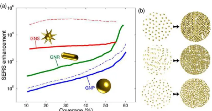
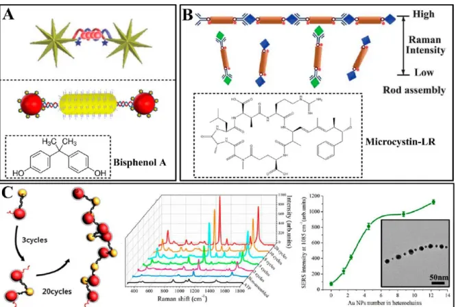
example, state-of-the-art electromagnetic computation techni-ques were used to simulate NP-based SERS substrates, comprising hundreds of randomly organized gold NPs. The authors unexpectedly concluded that NP morphologies that provide large enhancements at the single-particle level, such as nanostars, do not necessarily improve when organized in close-packed arrays; in contrast, simpler morphologies (e.g., spheres or rods) lead to significantly increased SERS enhancement as their surface density approaches full coverage (Figure 2).19
In addition to EM enhancements that can be calculated by solving Maxwell’s equations for specific nanostructures, more
qualitative estimates of EFs based on simple model structures (such as spheroids) have been developed25and, recently, used
to understand SERS for randomly rough substrates made of aluminum, gold, or silver over a wide range of wavelengths from the ultraviolet (UV) to the near-infrared (NIR), in good agreement with experimental data.26Prediction of plasmonic
properties of NPs with arbitrary morphologies has also been recently simplified by derivation of analytical expressions based on parameters that stem from numerical modeling.27,28 Nonlocal effects can also play a role in the EM mechanism;29,30
for example, although gaps between NPs lead to EM hotspots that often dominate SERS measurements (leading to SM sensitivity31), and although classical electromagnetics predicts that enhancements should vary inversely with the gap size,32
for gaps with dimensions significantly below 1 nm, quantum effects associated with electron tunneling between NPs become important,21,33,34 changing the dominant plasmon energies significantly, usually resulting in a reduction in the EM enhancement.
Surface-Enhanced Raman Scattering Mechanisms: Chemical. The chemical mechanism of SERS refers to contributions to the Raman scattering that do not rely on the EM environment (e.g., plasmon excitation), often because they are associated with the transfer of electrons between adsorbed molecules and the NP substrate. This can arise in two ways, corresponding to electron transfer in the ground and excited states of the molecule−metal system. The EF associated with the former mechanism can be defined in terms of the static polarizability derivatives of the molecule− metal system,35which is a property that can be calculated using
electronic structure theory using a cluster model for the metal particle, in which the particle is replaced by a small cluster of metal atoms. This type of calculation produces a result that is nominally independent of frequency, which reflects changes in the polarizability derivative due to the transfer of charge by the molecule adsorbed on the metal NP. Valley et al.36 obtained values from such calculations for several substituted benzene thiolates adsorbed on silver and gold substrates and compared them to measured EFs. Because the substrates were the same for all of the molecules considered, the variation in EF for the various molecules was entirely due to changes in the chemical enhancement. Theory and experiment were in agreement within a factor of 2, and the values that showed a variation of ∼10 for the molecules considered corresponded to a chemical enhancement in the 10−100 range.
Although the static polarizability derivative provides a simple way to model the chemical effect, including charge transfer (CT) in the optical frequency response is necessary for a complete understanding.37,38Charge transfer is challenging to estimate, however, as CT states are poorly described with standard density functional theory (DFT) methods and strongly mixed with plasmon excitations in models that couple molecules to metal clusters. Thus, separating CT effects from plasmon excitations is not rigorously possible. One way to make progress involves the use of semiempirical molecular orbital methods, such as INDO/S,39 with parameters appro-priately chosen to give reasonable plasmonic properties for Ag.40With this approach, it is possible to describe CT effects accurately and to separate CT and plasmonic contributions to SERS for molecule/cluster models. Such a separation was performed by modifying the INDO/S calculation so that terms in the Hamiltonian responsible for CT between molecule and metal were omitted, thereby yielding an electronic structure that only includes EM effects. The CHEM factor is then generated by comparing results with and without CT for frequencies where plasmon excitation occurs. In a study of the pyridine SERS spectrum on a silver cluster, this analysis generated a CHEM EF of 10 for excitation near the plasmon resonance.41It was also noted that there was a CT excited state ∼0.5 eV above the plasmon state and that this state produced a substantial Raman enhancement (down by a factor less than 10 from the SERS enhancement) when the CT state was excited on resonance. The significant enhancement associated with CT states provides rationalization for recent studies in which large Raman enhancements were observed for systems composed of organic molecules on organic semiconductor substrates, for which plasmon excitation is not present.42
Figure 3 shows a recent result based on semiempirical INDO/S calculations, for a CO molecule attached to a silver tip, in TERS.43 The Ag-CO tip was located near a gold substrate (see inset inFigure 3) under electrical bias, and the Raman intensity of the CO stretching vibration was measured as the bias was varied, resulting in an increased measured intensity with increasing bias above zero. Results for three different theoretical models of this experiment are plotted, all based on INDO/S with various approaches to defining how the bias induces a static potential between the tip and the substrate. The calculations show that the intensity increase stems from CT excited states that tune into resonance as the bias becomes more positive. Thus, we directly see how CT excited states can influence SERS intensities. The same theory can also be used to connect SERS measurements to formal potentials for TERS-based SM electrochemical studies.44,45
Figure 2. Predicted SERS enhancement as a function of surface coverage, for monolayers of gold NPs with different shapes (a). Solid curves obtained for excitation at 785 nm light wavelength (resonant with 65 × 21 nm nanorods); dashed curves obtained for 633 nm (resonant with 51 nm nanospheres) and 900 nm (resonant with nanostars: 20 nm core, 10 nm branches). Schemes in (b) illustrate low- and high-density NP surface coverage. Reproduced from ref19. Copyright 2017 American Chemical Society.
We note that the Ag-CO TERS measurement can also be performed by monitoring the shift in CO vibrational frequency instead of Raman intensity as a function of potential bias, and exciting developments have also been reported using the Ag-CO system for atomic resolution imaging.46
Modeling of Molecular Species at the Surface. Another challenge for theory in SERS involves the determi-nation of spectra using computation, which possesses sufficient precision to be used to determine the identity of the molecules producing them. This activity is important in almost any study where the identity of the species represented in the SERS spectrum is required and especially so when SERS is used to study chemical reactions on surfaces. Raman spectra can be generated for isolated molecules using various electronic structure codes; however, much uncertainty exists as to what structural model should be used in the calculations. As noted in the previous example, properly describing the chemical EF requires an electronic structure calculation that includes the molecule plus a metal cluster representing the plasmonic metal. The choice of cluster model is important, and, for any model, there are important questions as to which density functional is best47and what level of averaging over molecular orientations
on the cluster is needed to generate a meaningful result to be compared with experiment.48Ultimately, an exhaustive study
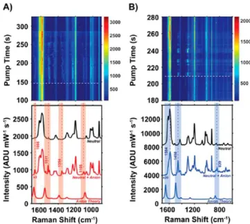
requires significant computational resources, and, given the level of uncertainty about what molecules are actually present, their protonation and charge state, and possible decomposition pathways, such studies soon become intractable. A greatly simplified approximation that often works well is to calculate the orientation-averaged spectrum associated with the molecule in the absence of any metal atoms using a simple functional like CAM-B3LYP.Figure 4shows an example of this type49for the molecule bipyridine (BPY), including results for both the H8and perdeutero D8isomers (where D8is used to determine if the spectra arise from single molecules or not). The top panels show waterfall spectra associated with experiments in which initially a relatively intense pulse of 532 nm light is used to irradiate BPY on a gold substrate for a
few seconds, followed by SERS spectra measured with 785 nm every few seconds for hundreds of seconds after the pulse. The top spectra in the lower panel are spectra measured for H8and D8, which are in excellent agreement with orientation averaged spectra for BPY calculated using DFT (not shown). The second spectrum shows the presence of additional modes (also seen in the waterfall plots) indicating the presence of another molecule. The bottom spectra in Figure 4 show calculated spectra for anions of the H8and D8molecules, which are open-shell molecules with low-lying excited states. The calculated spectra match the extra peaks that show in the middle panel, which enables the identification of the extra molecules as anions. This recently developed capability for generating resonance Raman spectra of this type using the NWChem program can clearly play an important role.49Ultimately, this
work and a more recent study of the molecule trans-1,2-bis(4-pyridyl)ethylene (BPE)50 demonstrate that 532 nm light
generates electrons that escape from the NPs and diffuse on the surface, occasionally converting the molecules to anions, sometimes with other conformational changes that include isomerization, as observed in the SERS spectra. The fact that the orientation-averaged spectra work well in this appli-cation is likely a reflection of the fact that the molecules being observed adopt many orientations on what is a randomly roughened SERS substrate and that many of the molecules that contribute to the results are not strongly coordinated to the metal surface. The foregoing illustrates how SERS can be
Figure 4. Representative anion events for both BPY-h8and BPY-d8. (A) Top waterfall plot depicts time-dependent SERS data as a function of optical pump time. Anion modes appear starting at 148 s, indicated by white dotted line. Bottom plot shows the neutral spectrum for a BPY-h8 + BPY-d8 nanosphere assembly (black); the midspectrum depicts the contribution from neutral molecules plus BPY-h8anion modes that appear (red); the bottom spectrum shows open-shell DFT (CAM-B3LYP) calculation for the radical BPY-h8 anion. (B) Waterfall plot from a different nanosphere assembly that shows a preference for BPY-d8anionic behavior, with anion activity appearing at 209 s of pump time. The top spectrum in the lower plot consists of neutral molecules only (black); the midspectrum is neutral plus BPY-d8anion modes; the bottom spectrum is DFT (CAM-B3LYP) calculated BPY-d8anion modes. Reproduced from ref 49. Copyright 2017 American Chemical Society.
Figure 3. Comparison of experiment (top) and theory (bottom) for the CO tip-enhanced Raman scattering intensity associated with an Ag-CO tip structure near a gold surface, as a function of potential bias. (inset) The tip model. Adapted from ref 43. Copyright 2018 American Chemical Society.
used to study molecular surface chemistry using relatively simple modeling.
Modified Electronic Absorbance of Molecules on Surfaces. Many SERS studies have been and still are being performed with analytes under resonant or preresonant condi-tions. The main reason for this choice is practical: Raman cross sections are much larger (typically by a factor of 102−106) than in nonresonant conditions,51 yielding stronger signals for a
given SERS EF, facilitating fundamental studies of SERS, notably in the context of SM detection.52 Other applications
also benefit from increased signals, for example, the use of SERS tags.
One consequence of using (pre)resonant analytes is that any change in electronic resonance originating from the molecule’s adsorption to the metal can dramatically affect the SERS measurements and their interpretations. In simplified terms, a spectral shift toward the excitation wavelength increases the Raman cross section of the adsorbed molecule, with respect to its intrinsic cross section, resulting in an apparent increase in the SERS EF, which operates in addition to the standard EM enhancement53and surface selection rules.54,55And vice versa for a spectral shift toward the excitation wavelength. Such a change in Raman polarizability upon adsorption can be classified as an instance of chemical enhancement,56,57which,
however, has been largely overlooked, as it could only be indirectly inferred from the SERS EF, which is affected by many factors.
Recent progress in experimental methods has enabled direct access to the modified absorbance spectrum of dye molecules such as rhodamine 6G (R6G) and crystal violet (CV) adsorbed on metallic NPs (Figure 5), a first important step toward assessing the effect of adsorption to the metal surface on their SERS response. These experiments have revealed three important points, discussed below in the case of R6G:
• The measured absorption enhancement is somewhat smaller (∼4 on 60 nm silver nanospheres) than expected from a simple isotropic EM model (the average surface absorbance enhancement is here predicted to be ∼15), which can be attributed to orientation effects59,60 and provides a complementary insight on the importance of preferential orientation in adsorption for quantitative or even semiquantitative interpretations of SERS exper-iments.
• The absorbance spectrum of the adsorbed dye is shifted, from ∼526 to 538 nm in the case of R6G. This relatively small shift could be explained by a chemical interaction61 or even by a purely EM interaction (image-dipole effect)60 with the metal surface. Such a shift in electronic energy is nonetheless likely to affect the (resonance) Raman cross section by a non-negligible factor: the Raman cross sections of bare R6G drop by a factor of 103−104from 532 nm (resonant) to 633 nm (preresonant) excitation51,62a 12 nm red-shift in resonance may therefore result in a measurable increase in cross section at 633 nm. Although these effects have not yet been evidenced directly in the SERS EF, they may explain why R6G has been so extensively used in SERS studies at 633 nm excitation on silver particles, even though its Raman cross section is relatively small at this wavelength.51 For molecules such as CV, where a dramatic change in the absorption spectrum is observed upon adsorption on silver, with a peak shift from 590 to
500 nm (Figure 5a), even more substantial changes in SERS EF can be expected.
• The absorbance spectrum varies with dye concentration, with spectral changes observed from a surface coverage as low as 0.1 nm−2 for R6G. This variation may be attributed to electromagnetic dipole−dipole interaction between adsorbed dyes on the surface and is akin to the spectral changes observed in the formation of J- or H-type dimers or aggregates of dyes. This interpretation is further supported by recent theoretical developments in the electromagnetic modeling of anisotropic shells of dyes.59,60,63 The implications of such dye−dye inter-actions in SERS have not yet been investigated but could be important. It is generally assumed that SERS enhancements are independent of analyte concentration, at least in the low-concentration regime, where there is no saturation of adsorption. Many studies have therefore used average SERS signals as a proxy for the number of adsorbed molecules, for example, to study adsorption isotherms. Dye−dye interactions may affect these interpretations, and further work is needed to assess their contribution in concentration-dependent SERS experiments.
These recent results call for additional experiments, comple-mented by EM theory and computational chemistry,61,64 to refine our understanding of this chemical enhancement contribution to SERS and how it is affected by the parameters that govern adsorption of specific molecules: their adsorption geometry, relative orientation, (in-)homogeneity in surface coverage, and how much the electronic resonance is affected
Figure 5. (a, b) Measured differential absorbance spectra of CV and R6G adsorbed on 60 nm silver nanospheres at low surface coverage, compared with the reference absorption spectra in water. (c) Extinction and absorbance spectra of the silver nanospheres (at 8 pM) compared with the bare R6G spectrum in water. (d) Concentration dependence for the modified absorbance spectra of R6G on 60 nm silver nanospheres. See ref 58 for further experimental details.
by adsorption. Pushing experiments to the UV region will be highly desirable in this context, to probe the chemical changes undergone by a wider range of relevant molecules. It will also be instructive to consider different types of NPs (silver, gold, but also dielectric and core−shell particles) with diverse shapes, to explore more comprehensively the full range of molecule−surface interactions. Such studies also have direct relevance to the pursuit of weak and strong coupling between local emitters and NPs that sustain strong plasmonic or Mie resonances, a topic of current interest for applications in quantum optics,65 spasers,66 surface-enhanced
photochemis-try,67and circular dichroism (CD).68
Strong Coupling Regime.A recently introduced insight is the strong coupling regime between plasmons and molecular excitons under SERS activity. In 1997, SM SERS was discovered by EFs of 1010−1014 for dye molecules within plasmonic NP aggregates69,70and was successfully explained by
the EM model, under the condition that NP dimers included SMs at their junctions.71 It was therefore concluded that the EM model is the dominant SERS mechanism. The NP dimers generating SM SERS enabled direct examination of various relationships between plasmons and SERS associated with the EM model, because in this strategy, one can identify the plasmon “resonance” that is inducing Raman “enhancement” by single-particle spectroscopy.72 These examinations also highlighted phenomena involving SERS hotspots, as follows: (1) Spectral changes in plasmon resonance by losing SERS activity revealed that SERS hotspots may involve strong coupling, in which EM coupling rates between plasmon and molecular exciton resonances are larger than the dephasing rates of both resonances. (2) The unusual laser energy dependence of broad background emission spectra in SERS was revealed as ultrafast surface-enhanced fluorescence (ultra-fast SEF), in which SEF rates exceed the molecular vibrational decay rates, thus resulting in emission from vibrationally excited states in the electronically excited state. (3) The appearance of forbidden Raman modes in SERS spectra was revealed as the breakdown of the selection rules of Raman excitation by the field-gradient effect. These three insights are related to the strong coupling regime; thus, for future perspective the initially proposed EM in SERS model should include these points to more appropriately explain the SERS effect at hotspots.
The main point for considering strong coupling regimes in SERS is estimating the size of hotspots that generate SERS. Various efforts toward improving the EM model including strong coupling revealed that the size of hotspots can be below 1 nm3at the junction between NP dimers or NPs on flat metal surfaces.65 We present below these three topics. First, the correlation between strong coupling and ultrafast SEF has been also investigated as a function of the extremely small hotspot size.73 Second, in photochemistry, such an extremely small volume of the hotspots indicates that SERS may be useful to analyze the internal structure of SMs.74Indeed, SERS spectra
usually show spectral changes related to structural changes of SMs located at hotspots.75However, the perfect elucidation of such structural changes is quite difficult, because reference data for assignment are lacking. Therefore, DFT calculations are helpful to analyze SM structural changes induced by oxidization, local decomposition, etc. Third, in photophysics, SM SERS at extremely small hotspots indicates that (ultra- and deep-) strong coupling can directly control the ground-state
properties of the molecule, because such changes by ℏg
N
2 1
cannot be negligible for an SM condition, where ℏg is the coupling energy, and N is the number of molecules involved in the coupling.76Thus, under the SM strong coupling condition, a conventional nonresonant excitation condition can become resonant, thereby resulting in a photochemical reaction by applying energy below the conventional excitation energy threshold and/or in nonlinear optical responses such as the pumping effect and classical Rabi splitting driven by photons. Ultrafast SEF reveals the control of excited-state electron dynamics of SMs at hotspots.77
Controlling the size of hotspots is important for the investigation and application of strong coupling in SERS; however, note that the size of conventional (zero-dimensional) hotspots may be too small for application in practical devices, utilizing the above-mentioned photochemical and photo-physical phenomena. Thus, we expected that special types of hotspots would be developed that can resolve the size problem. One example is provided by one-dimensional hotspots along the junction in nanowire (NW) dimers or between NWs and flat metal substrates.78 The two main characteristics of such hotspots are (1) the volume is considerably larger (at least 104 times) than hotspots within NP dimers and (2) hotspots can interact with propagating plasmon modes. The larger volume of hotspots makes SERS phenomena stable by mitigating the effect of molecular fluctuations. Interaction with propagating plasmons may enable transfer of information at hotspots in NW network systems, including zero- and one-dimensional hotspots. We propose that research in this direction, that is, considering the strong coupling regime and its extentive phenomena including the control over the size of hotspots, will lead to novel photoscience and phototechnology in SERS.
Extreme Interaction Regime (Quantum Effects). For many years, the SERS signal from a few or even SMs has been described as being due to the local field produced in the vicinity of the pristine host nanoantenna, and the EFs were obtained from standard electrodynamics methods, within the local dielectric response theory.32,79This initial classical descrip-tion provided the main spectral features of the plasmonic gap,71,80,81including its spectral dispersion as the gap closes as
well as the dependencies of the intensity of the corresponding local fields. This approach provided a fundamental under-standing of the classical regime of interaction and served to interpret numerous SERS experiments of molecules in colloidal solution and in TERS configurations. However, synthesis and fabrication methods have improved their capabilities to build plasmonic nanoantennas, currently being able to reach gaps down to a few nanometers and below 1 nm, where molecules and material layers can be located.82In this extreme regime of interaction, quantum effects due to the dynamics of the electron gas forming the plasmon mode are revealed, and their description requires theoretical approaches beyond classical electrodynamics, as pointed out in the sections above.
An adequate approach to address the optical response, and thus the local fields of plasmonic gaps at this extreme regime, relies on solving the time-dependent Schrödinger equation for the dynamics of the electron gas forming the gap. Such an approach turned out to be very valuable to set the limits of classical electrodynamics and to account for the actual field enhancements in the cavity. In particular, a quantum-mechanical treatment of the optical response, at different levels of accuracy, accounts for (i) dynamical screening effects in the
response, the so-called non locality;83(ii) the effect of spill-out of the electrons at interfaces that can extend spatially a few ångströms into the dielectric;84 (iii) quantum-size effects, which are relevant for small clusters and protrusions;85 (iv) atomistic effects, which sculpt the surface-charge density at sub-nanometer dimensions;86,87 and (v) optical tunneling, which sets conduction channels at optical frequencies even before physical contact between the metallic surfaces, thereby quenching and reshaping the distribution of the local fields34
sensed by the molecules and other sample materials.
This plethora of quantum effects get to their epitome when nanometer and sub-nanometer gaps with atomic-scale features are formed within a plasmonic cavity. Theoretical approaches attempted to face these challenges and describe the local fields and, thus, the SERS signal, in these extreme situations. A recent example showed how tunneling effects produced charge transfer between metallic interfaces in vacuum at ∼4 Å gap separation,34 quenching the local field, as experimentally confirmed.88,89However, most of the practical realizations of SERS in plasmonic gaps can still play safe, as most nanogaps used in SERS are larger than half a nanometer, thereby avoiding the onset of tunneling effects. Nevertheless, some conducting molecules might distort this general rule of thumb,90,91 and conduction effects between electrodes at optical frequencies might be a matter to be considered more deeply in the future.
In the realm of sub-nanometer plasmonic gaps, the challenges for accurate modeling are diverse, and in one way or another, many of them have to do with the quantum description of either the plasmonic gap, the material sample, the type of interactions, or all together. A remarkable experimental achievement in a TERS configuration managed to obtain optical Raman maps for selected vibrational modes of a single molecule with sub-nanometer resolution,74thus even competing with the signal obtained in STM. This level of resolution required a previously unthinkable localization of the local fields within the gap, far beyond the typical 5−10 nm lateral plasmonic extent within the gap. Accurate atomistic ab initio calculations based on time-dependent DFT (TDDFT), which considered the actual distribution and configuration of atoms within a gap, revealed that atomic-scale localization of the fields was indeed possible,87thanks to the varying induced
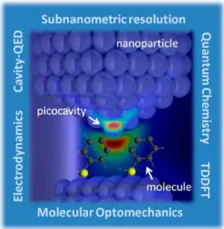
electronic density profile at single atoms acting as an atomic-scale lightning rod.92 The actual field localization in such a
situation is shown in Figure 6. The simplicity of the concept provides an effective description of this effect by classical means, where atomic protrusions in a cavity can be modeled by corresponding classical interfaces that follow the electronic density profile.93 Such an extreme localization, as it may
happen in many tip apexes, might be responsible, to a large extent, for the sub-nanometer resolution achieved in an increasing number of experimental TERS realizations.74,94−96
This extreme localization not only affects resolution but also actually governs a dramatic breaking of Raman selection rules at the SM level due to the action of the strongly inhomogeneous fields induced at atomic-scale morpholo-gies.97−99
Activation of unusual vibrational modes of SMs under stable conditions has been reported in both cryogenic74,99 and room-temperature conditions.100,101 Most such features can only be explained in terms of this extreme atomic-scale field localization within the gaps, which have been termed “picocavities” due to the ultrasmall effective mode volume sustained by the atomic features (seeFigure 6).
An additional challenge of the current modeling and under-standing of the Raman processes is associated with the possi-bility of exploiting the optomechanical interactions between molecular vibrations and plasmons, beyond the thermal regime. The recently established analogy between nonresonant Raman scattering and an optomechanical process102 has enabled a description of the dynamics of plasmons and vibra-tions in SERS, within the framework of cavity quantum electro-dynamics (QED), with the use of a linearized interaction Hamiltonian Ĥint= −ℏgo(â†â)·(b†+ b), where â†,â (b†,b) are the plasmon (phonon) creation, annihilation operators, and go is the vacuum optomechanical coupling, which is inversely proportional to the effective mode volume of the plasmonic cavity, go ∝1/Veff. This quantum treatment has predicted a nonlinear evolution of the Stokes and anti-Stokes Raman signals, due to the optomechanical interaction.103 Such an effect has been revealed in molecules in the vicinity of plasmonic picocavities, which boost the optomechanical interaction, go, as a result of the extremely reduced effective mode volume.91 Molecular optomechanical pumping or cooling in plasmonic cavities can overcome thermal effects,104,105 thereby opening the possibility of controlling the vibrational dynamics and reactivity of molecules.106
Therefore, many unusual trends and variations of vibrational lines in plasmonic SERS might now be reinterpreted in terms of optomechanical interactions. The effort to describe theoretically this rich variety of molecular optomechanical effects in realistic plasmonic cavities results in the cavity-QED framework.107 Cooling and pumping of vibrational modes,
resonant Raman processes, collective effects due to self-assembly of molecules within plasmonic gaps, or the statistics of Stokes and anti-Stokes emissions are theoretical and experimental challenges that the SERS community will need to face sooner or later.
Another important issue in the theoretical description of SERS has to do with the assumption of physical interac-tions between sample (molecule) and cavity (plasmonic gap).
Figure 6. Artist’s view of a plasmonic gap formed by metallic nanoparticles hosting a set of organic molecules. A picocavity is formed due to the protrusion of a single atom, localizing the electromagnetic field at the atomic scale, thus producing sub-nanometer resolution and close-to-strong optomechanical cou-pling. Theoretical methods to address this extreme interaction regime in surface-enhanced Raman scattering are outlined on the sides, including electrodynamics, cavity QED, quantum chemistry, and TDDFT.
In practice, chemisorption of molecules on metallic surfaces often produces a complex redistribution of the molecule− substrate electronic structure and, thus, of its corresponding polarizability, modifying vibrational modes and enabling charge transfer.108 This effect complicates the modeling and simple description of Raman modes as well as the depend-encies of their intensities, and it might require a combined quantum description of the substrate−molecule hybrid, together with the self-consistent action of the induced EM field at the cavity. In other words, the quantum realm of vibrational spectroscopy in extreme atomic-scale cavities might require the combination of aspects from condensed matter physics, quantum chemistry, and classical or quantum nano-optics, which turn SERS into a fascinating arena for theoretical developments, as well as for experimental testing and exploitation of unexpected effects.
Outlook for Future Surface-Enhanced Raman Scat-tering Applications.Research during the past few years has opened opportunities for further intriguing SERS science and technology, which, in our view, has been enabled by the emerging capability to use bottom-up nanoassembly in a reproducible, robust manner to form nanometer-sized gap constructs. Let us consider two regimes, with either few or specific numbers of molecules in a fully defined nanoscale geometry, or a paradigm for simple but robust solution-based SERS sensing.
The first is the nanoparticle-on-mirror (NPoM) construct, which produces single gaps down to 0.3 nm between two plasmonic metals that can be precisely filled with different molecular or monolayer systems (for a recent review of this system see ref 109). It can be understood as a metal− insulator−metal (MIM) waveguide that confines light, both between the metals and laterally, to give less than 50 nm3 mode volumes. This system has improved understanding of the role of molecular conductivity on SERS,91as well as aided in identifying the origins of SERS background emission (which sets practical detection limits) as coming (partly) from molecule−metal coupling110 and partly from the unavoidably enhanced electronic Raman scattering of free electrons in the metal walls.111,112Careful kinetic studies of NPoMs show that optically induced migration of individual metal atoms dominates much of the dynamics,113 which can even induce
metallic nanowires to bridge across the gap, changing both plasmon resonances and SERS.114,115 This work has been
extended to look at memristive electronic memory devices,116 to study individual charges hopping on and off single redox molecules117 (which shifts the SERS lines), and to study the influence of electrochemical potentials on SERS.118It has also been demonstrated that single emitters can be precisely assembled in NPoMs using DNA origami, thereby enabling SERS of strong coupling systems.65,119This and many ongoing
experiments reveal much of the nanoworld at interfaces, showing it to be far more subtle, nuanced, and dynamic than previously accepted.
A detailed campaign to study the SERS of NPoMs has revealed the presence of transient sharp vibrational lines that evolve. With an apparatus devised to drop the laser power automatically as soon as these are detected and initially at cryogenic temperatures, it was shown that the transient SERS must originate from single molecules in the gap.99A variety of evidence showed that single Au atoms move partially out of the close-packed metal surface to yield extra field enhance-ments of 3−5. Therefore, several-hundred-fold higher SERS
enhancements enable SMs to emit more signal than the remaining hundred molecules in the gap.105,106 These
observations also resolve questions from past decades, such as the spatial mapping and irreproducibility of TERS, as well as how SM signals can be observed in SERS, likely emerging from picocavities in the crevices of aggregated metal NPs (though much less controllably). The same Au adatom behavior was also recently shown at room temperature, using several million SERS spectra to prove that the atom prefers to move from the bottom planar Au mirror,101 at least in some cases. The
prospects for intriguing light−matter and catalytic interactions in such atomic-scale regions are fascinating and ongoing.
The second regime of interest has been the use of colloidal metal NP aggregates when the gaps are set by precise linkers (e.g., cucurbit[n]urils, giving 0.9 nm gaps), which can filter classes of small molecules from a heterogeneous soup into SERS active reliable hotspots. This technology facilitated the detection of neurotransmitters at clinical concentrations in urine120 and of methanol at less than 1% in ethanol,121 and these assays are also used in microdroplets122,123 and
microfluidics.124This technology can be used to track chemical reactions routinely125and, thus, is now ripe for exploitation, for example, in the form of the “Intelligent Toilet”, capable of long-term personalized health monitoring. The ability to explore fundamental science at the nanoscale through SERS of individual, exquisitely controlled nanoassemblies, as well as developing realistic societal tools for personalized medicine and other challenges, puts SERS in great shape for continuing developments (Figure 7).
SURFACE-ENHANCED RAMAN SCATTERING SUBSTRATES
An important prerequisite for better understanding of SERS and its applications in chemical analysis and SM detection is the development of highly reproducible, reliable, and rational substrates. “Rational” in this case means that the substrate has quasi-uniform and predictable optical and near-field properties. The choice of the substrate type, material, and fabrication method depend on the specific application or question to be answered. More fundamentally and academically oriented problems, such as the question of the dependence of SERS EFs on hotspot size/geometry, require fabrication methods to tune the plasmonic structure (at the single-particle level), pushing
Figure 7. Structures ranging from nanogap geometry (NPoM) to nanoparticle sensing using CB:AuNP aggregates enable surface-enhanced Raman scattering applications from single-molecule detection to personalized medicine.
the precision to ultimate limits that are usually time-consuming, costly, and hardly possible to produce at large scales. However, when focusing on (practical) chemical analysis, aspects other than high precision are important, for example, large-scale homogeneity and batch-to-batch reproducibility of the substrate, cost-effective and easy fabrication, robust SERS signal intensity, substrate stability, high affinity toward the analyte of interest under given conditions, etc.
In this context, the concept of SERS substrates does not only refer to solid substrates but also to colloidal NPs in a dispersion medium (solution). Advantages of using colloidal NPs include highly reproducible and cost-effective synthesis via bottom-up strategies, tailored optical properties over a wide wavelength range by tuning particle shape and size, as well as manifold surface functionalization, which render them applicable in different environments and for many analytes. The most widely used NPs display a simple spherical morphology, at the expense of exhibiting moderate Raman signal enhancement as single particles because of their high symmetry. Aggregated colloidal NPs still feature low cost while often exhibiting very strong enhancement due to a three-dimensional (3D) distribution of plasmonic hotspots. How-ever, since colloidal aggregation is a dynamic process, SERS spectra must be recorded within a certain time window, meaning that the reproducibility of the SERS spectra strongly depends on the precise experimental conditions used. In contrast, anisotropic plasmonic single NPs enable substantial Raman signal enhancement, due to the presence of intrinsic hotspots at edges and corners, such as in nanorods (NRs) and nanocubes, or at sharp protruding features, such as in nanostars. Among all other shapes, gold nanostars have likely attracted the most attention recently: their validity as effective SERS enhancing platforms was proven early on and has been a motivation to pursue the investigation of their properties further over the past decade.126−131Within the general concept
of nanostars, we consider a variety of geometries and symme-tries, and, therefore, we dedicate a section below to discuss this particular shape class exclusively.
Although colloidal systems pose the potential problem of aggregation in solution, this drawback can be overcome by directing the self-assembly of colloidal nanoparticles into homogeneous and ordered layers and arrays. Multilayered systems and supercrystals offer substrates with three-dimen-sionally organized hotspot architectures. Alternatively, sophis-ticated colloidal lithography and chemical etching methods can be also applied. These methods all enable the hotspot size, geometry, and density to be designed and engineered in a reliable manner, over large areas. Some of the reported assembly strategies enable the fabrication of substrates that are not just restricted to flat supports but can also be applied to flexible, curved, or rough supporting materials, thereby leading to sensing applications.
The renewed drive to expand the materials base for plasmonics beyond the coinage metals and aluminum, motivated by both extension of localized plasmon resonances into the infrared (IR), as well as issues around loss, tempera-ture stability, and complementary metal−oxide−semiconduc-tor (CMOS) compatibility,132 is expected to also have an
influence on the development of substrates for SERS.133 Transition-metal nitrides, transparent conductive oxides, metal sulfides, and doped oxides are all candidate materials for future surface-enhanced spectroscopy substrates, and a survey of these materials from this point of view is warranted.
Surface Chemistry, Stability, and Solution-Phase Nanoparticles: A Balancing Act.Nanoparticles synthesized using bottom-up synthetic methods are widely used as SERS substrates. Most often these materials are synthesized via metal-reduction routes in the presence of electrostatically stabilized chemical species, dynamic stabilization using molecules or ions with reversible affinity for an interface, or covalently attached surface ligands. Each of these surface chemistries offers different advantages and disadvantages for subsequent SERS applications, as these surface chemistries simultaneously promote the suspension of the nanostructures in solution, lead to the formation of EM hotspots for increased SERS signals,134 and/or can block the metal surface from adsorption of the targeted molecules when used for direct detection.135 The latter mechanism can limit direct SERS detection because of signal suppression arising from short-range chemical enhancement mechanism routes associated with SERS. Solution-phase NPs are inherently “metastable”, because colloidal dynamics induce frequent collisions between nanostructures due to Brownian motion.136,137These materials can remain stably suspended in solution for long periods of time, yet they can also undergo degradation through dissolution,138−140aggregation,136,137and/or sedimentation141
processes during storage and/or use. Although dissolution is dependent on electrical potential differences between the metal nanoparticle composition and other chemical species in solution, both sedimentation and aggregation depend on the dynamic movements of nanostructures in solution. The kinetics of these processes can be modeled using collision theory.142,143 In so doing and by treating nanostructures as
point charges moving in three dimensions in water at room temperature, it is estimated that over ∼104particle collisions will occur per second in a 1 mL solution containing ∼5 nM nanostructures.137 The energetics involved with the collisions will dictate whether nanostructures aggregate, forming potential hotspots for large SERS enhancement, generating relatively larger aggregates in solution that can lead to EM losses and particle sedimentation if the mass of the aggregates overcomes buoyancy forces or remains stably suspended in solution, thus exhibiting plasmonic properties that are maintained.
Surface chemistry and the local environment surrounding nanostructures in the solution phase control the energetics and fate of these materials for SERS applications. Both molecule orientation and dwell time at high-field-strength locations must occur, suggesting that adsorption is required.135 In addition, the energetics of nanoparticle collisions must be considered, because these influence the underlying plasmonic properties and enhancement associated with SERS substrates.144In other
words, both chemical and EM enhancement mechanisms influence the observed spectroscopic signal, and these both depend on the local environment surrounding the nanostruc-tures and their surface chemistry. The probability of observing an SERS signal for a given molecule increases as the analyte exhibits more favorable binding energies and nonzero sticking probabilities to an interface.145,146Many parameters including
material composition, solvation, and local surface chemistry can either promote or prohibit the sticking probability of a molecule. In general, SERS signals are detectable for a given molecule, if that molecule exhibits a larger attractive potential to the surface versus its incident kinetic energy, thus increasing its residence time at the interface and exceeding the collection time window for an SERS measurement.135It is well-established