Publisher’s version / Version de l'éditeur:
Vous avez des questions? Nous pouvons vous aider. Pour communiquer directement avec un auteur, consultez la première page de la revue dans laquelle son article a été publié afin de trouver ses coordonnées. Si vous n’arrivez pas à les repérer, communiquez avec nous à [email protected].
Questions? Contact the NRC Publications Archive team at
[email protected]. If you wish to email the authors directly, please see the first page of the publication for their contact information.
https://publications-cnrc.canada.ca/fra/droits
L’accès à ce site Web et l’utilisation de son contenu sont assujettis aux conditions présentées dans le site LISEZ CES CONDITIONS ATTENTIVEMENT AVANT D’UTILISER CE SITE WEB.
Physical Review Letters, 120, 13, 2018-03-27
READ THESE TERMS AND CONDITIONS CAREFULLY BEFORE USING THIS WEBSITE. https://nrc-publications.canada.ca/eng/copyright
NRC Publications Archive Record / Notice des Archives des publications du CNRC :
https://nrc-publications.canada.ca/eng/view/object/?id=f9599632-84c2-4040-8c9b-2a73ae61ecc4 https://publications-cnrc.canada.ca/fra/voir/objet/?id=f9599632-84c2-4040-8c9b-2a73ae61ecc4
Archives des publications du CNRC
This publication could be one of several versions: author’s original, accepted manuscript or the publisher’s version. / La version de cette publication peut être l’une des suivantes : la version prépublication de l’auteur, la version acceptée du manuscrit ou la version de l’éditeur.
For the publisher’s version, please access the DOI link below./ Pour consulter la version de l’éditeur, utilisez le lien DOI ci-dessous.
https://doi.org/10.1103/PhysRevLett.120.136402
Access and use of this website and the material on it are subject to the Terms and Conditions set forth at
Charge-spin correlation in van der Waals Antiferromagnet NiPS3
Kim, So Yeun; Kim, Tae Yun; Sandilands, Luke J.; Sinn, Soobin; Lee,
Min-Cheol; Son, Jaeseok; Lee, Sungmin; Choi, Ki-Young; Kim, Wondong; Park,
Byeong-Gyu; Jeon, C.; Kim, Hyeong-Do; Park, Cheol-Hwan; Park, Je-Geun;
Moon, S. J.; Noh, T. W.
Charge-Spin Correlation in van der Waals Antiferromagnet NiPS
3So Yeun Kim,1,2 Tae Yun Kim,2,3 Luke J. Sandilands,1,2,§Soobin Sinn,1,2 Min-Cheol Lee,1,2 Jaeseok Son,1,2 Sungmin Lee,1,2 Ki-Young Choi,1,2 Wondong Kim,4 Byeong-Gyu Park,5 C. Jeon,6 Hyeong-Do Kim,1,2
Cheol-Hwan Park,2,3 Je-Geun Park,1,2,*S. J. Moon,7,† and T. W. Noh1,2,‡ 1
Center for Correlated Electron Systems, Institute for Basic Science (IBS), Seoul 08826, Republic of Korea
2Department of Physics and Astronomy, Seoul National University (SNU), Seoul 08826, Republic of Korea
3
Center for Theoretical Physics, SNU, Seoul 08826, Republic of Korea
4Korea Research Institute of Standards and Science (KRISS), Daejeon 34113, Republic of Korea
5
Pohang Accelerator Laboratory, Pohang University of Science and Technology (POSTECH), Pohang 37673, Republic of Korea
6
Advanced Nano-Surface Group, Korea Basic Science Institute (KBSI), Daejeon 34133, Republic of Korea
7Department of Physics, Hanyang University, Seoul 04763, Republic of Korea
(Received 25 June 2017; revised manuscript received 29 September 2017; published 27 March 2018)
Strong charge-spin coupling is found in a layered transition-metal trichalcogenide NiPS3, a van der
Waals antiferromagnet, from studies of the electronic structure using several experimental and theoretical tools: spectroscopic ellipsometry, x-ray absorption, photoemission spectroscopy, and density functional
calculations. NiPS3 displays an anomalous shift in the optical spectral weight at the magnetic ordering
temperature, reflecting strong coupling between the electronic and magnetic structures. X-ray absorption,
photoemission, and optical spectra support a self-doped ground state in NiPS3. Our work demonstrates that
layered transition-metal trichalcogenide magnets are useful candidates for the study of correlated-electron physics in two-dimensional magnetic materials.
DOI:10.1103/PhysRevLett.120.136402
Layered van der Waals (vdW) materials, such as gra-phene and transition-metal (TM) dichalcogenides, have attracted much attention over the last decade [1–3]. A remarkable advantage of these materials is that they can be mechanically exfoliated to produce two-dimensional (2D) crystals[1–3]. The intriguing collective quantum phenom-ena found in 2D vdW materials include charge density waves and superconductivity [4–8]. These observations open a new approach for novel device applications through the manipulation of collective quantum states in atomically thin 2D phases[3,6,9]. Despite extensive research on vdW materials, it is striking that very few studies have focused on magnetic 2D vdW materials.
Only recently has attention focused on new magnetic 2D vdW materials of ternary transition-metal trichalcogenide (TMTC) families, such as CrBTe3 (B¼ Si or Ge) and
TMPX3(TM¼ 3d TMs; X ¼ chalcogens)[10–12]. These
TMTC samples exhibit various magnetic orderings: ferro-magnetic (FM), zig-zag antiferroferro-magnetic (AF), N´eel AF, and stripy AF [10–16]. Moreover, all three key magnetic Hamiltonians—i.e., Ising, XY, and Heisenberg types—are realized in TMPX3 [13–17]. Additionally, long-range
magnetic ordering has recently been reported to persist in the atomically thin limit, e.g., monolayer FePS3 and
bilayer CrGeTe3[10,14,18]. Thus, it has become clear that
the TMTC families, i.e., layered vdW magnets, are excel-lent candidates for exploring intriguing phenomena related
to 2D magnetism, which will ultimately pave the way for novel applications in spintronics.
Compared with other nonmagnetic vdW materials, these new magnetic vdW materials offer a unique opportunity to explore strongly correlated electron systems in the 2D limit. Electronic correlation physics has been widely investigated in TM oxides, where the coupling of charge-spin-orbital-lattice degrees of freedom leads to various emergent phenomena[19–21]. One of the most intriguing phenom-ena due to electronic correlations is observed in quasi-2D materials, i.e., high-transition-temperature (Tc)
supercon-ductivity [22,23]. Over the past few decades, researchers have attempted to unravel correlation physics in 2D materials of heterostructure interfaces and/or oxide ultra-thin films, and have reported a variety of interesting observations [24–28]. Layered magnetic vdW materials offer an interesting platform for exploring correlation-induced phenomena. Intrinsic magnetism in TMTC implies the presence of localized electrons, so correlation physics is expected in these vdW materials. The electronic structure of TMTC can provide insights into the electronic correla-tions in layered magnetic vdW materials. However, few experimental studies have focused on the electron corre-lation in TMTC.
In this Letter, we report on the electronic structure of bulk NiPS3 single crystal, a TMTC antiferromagnet in
closely related. Using optical spectroscopy techniques, we observed clear anomaly in the optical spectral weight at the N´eel temperature, driven mainly by the magnetic ordering, which is a hallmark of correlated electronic systems
[21,29]. Subsequent x-ray absorption and photoemission studies, along with cluster model calculations, also revealed that NiPS3 is a self-doped negative charge transfer (NCT)
insulator. That is, the ligand (sulfur ions) has a strong holelike character due to NCT energy, analogous to the hole-doped high-Tccuprates and Kondo insulators[30,31].
Such an intriguing electronic and magnetic ground state was also confirmed by density functional theory (DFT) with effective Coulomb interaction (Ueff) calculations. Our findings indicate that NiPS3is a unique vdW magnet
exhibiting clear evidence of strong correlation and NCT behavior.
High-quality single crystals of NiPS3 were grown by a
chemical vapor transport method, as described previously
[32,33]. For optical measurements, we used a 55-μm-thick single crystal and an M-2000 ellipsometer (J. A. Woollam Co.). Ni L-edge x-ray absorption (XAS) spectra were obtained using scanning transmission x-ray microscopy (STXM) at beam line 10A of Pohang Light Source (PLS) II. We carried out the DFTþ Ueff calculations using the Quantum ESPRESSOpackage [34,41–47].
NiPS3 is one of the transition-metal phosphorous
tri-chalcogenides (TMPX3) with an AF long-range ordering. It
has a monoclinic structure with C3
2hsymmetry and features
edge-sharing NiS6 octahedra arranged on a honeycomb
lattice[32,48]. At the center of the honeycomb lattice, two P atoms are located above and below the TM plane. They are covalently bonded to the S atoms, forming aðP2S6Þ
4−
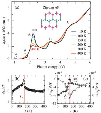
anion[48,49]. The magnetic moments of Ni ions are known to be aligned in a so-called “zig-zag” pattern; i.e., chains of ferromagnetically coupled spins are arranged antiferromag-netically [16], as shown in the inset of Fig. 1(a). Our in-plane magnetic susceptibility χðTÞ shows an AF magnetic anomaly at the N´eel temperature (TN∼ 154K) [Fig.1(b)].
The optical conductivity spectra σ1ðωÞ show that
NiPS3 is an insulator with an optical gap of about
1.8 eV [Fig. 1(a)]. At the same time, there are strong narrow absorption peaks near 2.2, 3.5, and 4.6 eV [labeled A, B, and C, respectively, in Fig.1(a)]. Below the gap, there are two additional weak peaks near 1.1 and 1.7 eV, denoted as α and β, respectively [see Supplemental Material (c-1)
[34]]. For comparison, NiO, which has the same formal valence of Ni (+2) as NiPS3, is reported to have weak
on-site d − d transitions at 1.13 and 1.75 eV[51]. Due to the similarities in the energy positions and strengths of the peaks, it is most likely that the α and β peaks are the on-site d − d transitions, a transition within one Ni ion. It should be noted that the hybridization of Ni 3d orbitals with S 3p can provide a much larger bandwidth than that with O 2p in NiO. Nonetheless, the narrowness of the A, B, and C peaks, in addition to the existence of the α and β peaks, suggests
the presence of well-localized Ni 3d orbital states near the Fermi energy (EF) in the electronic structure.
The optical conductivity of NiPS3 displays strong
temperature (T) variations. Note that peak A shows strong enhancement in intensity, while peaks B and C sharpen without much change in intensity upon cooling. To quantify the temperature evolution, we calculated the squares of the plasma frequency ω2p: ω
2 pðTÞ ¼
8Rσ1ðω; TÞdω [52], which we refer to as the spectral weight (SW). The optical sum rule is satisfied when we integrate up to 4.2 eV, implying the clear SW shifts from peak A to peaks B and C. At the same time, satisfaction of the optical sum rule indicates that most of the T-dependent changes in the electronic structure should occur near the Fermi level.
When we further examined the T dependence, we found clear anomaly in the SW changes of the main peaks occurring at TN. Figure1(c)shows the temperature
derivative of SW in the energy ranges of peak A (1.52– 2.63 eV) and of peaks B and C (2.63–5.00 eV). The former
(a) 0 6 8 2 4
Photon energy (eV)
1 2 3 4 5 6 A B C 1 ( ) (10 3 -1cm -1) 400 K 200 K 150 K 100 K 10 K 300 K 10 K 400 K 0 100 200 300 400 T (K) d || /dT 0 1 Zig-zag AF 0 100 200 300 400 T (K) 4 8 0 -4 -4 0 -8 -12 -1 d ( p 2)/ dT d ( p 2)/ dT (b) (c) TN A B/C ×10-5 ×10⁻⁵
FIG. 1. (a) Real part of the optical conductivity σ1ðωÞ of NiPS3
measured between 10 and 400 K[50]. The three main optical
transitions are labeled A, B, and C. Two weak on-site d − d transitions (α and β) are located below 2 eV. The inset shows the schematic diagram of the zig-zag antiferromagnetic ordering, where the honeycomb lattice of Ni ions is shown by black lines, and the spin is depicted as an arrow in each site. (b) The first derivative of magnetic susceptibility (χ) with respect to
temper-ature measured under in-plane bias fields on NiPS3. (c) The first
derivative of spectral weight ω2
p obtained for the energy range
of peak A (1.52–2.62 eV) and peaks B/C (2.63–5.00 eV). The
N´eel temperature of NiPS3(TN∼ 154K) is represented as a red
vertical line.
shows an abrupt change at TN, and the latter shows a
similar feature with the opposite trend, in which the shape is similar to the first derivative of χðTÞ shown in Fig. 1(b). The observation of the SW anomaly at TN is compelling
evidence of strong coupling between the electronic and spin structures in NiPS3.
Conventionally, most ground states of strongly corre-lated compounds can be categorized via the Zaanen-Sawatzky-Allen (ZSA) classification scheme [53,54]. Depending on the relative size of on-site U and charge-transfer energy (Δ), the insulating ground state can be classified as either Mott-Hubbard or charge-transfer insula-tors. However, there is a less explored region in the ZSA scheme where compounds can have NCT energy (Δ < 0). In this region, electrons of the ligand p orbital transfer to the TM d levels in the ground state, creating holes at the ligands without external doping. Thus, these compounds are often referred to as “self-doped”[55]. The ligand hole can contribute significantly to the conductivity and magnet-ism[30]. To some extent, the nature of the self-doped state is analogous to the ground state of the Zhang-Rice singlet states found in hole-doped cuprates [34,56,57].
Indeed, this interpretation of the self-doped ground state agrees with XAS and XPS results of NiPS3. We obtained
the Ni L2;3 edge XAS spectra of bulk NiPS3, which were
subsequently analyzed using a cluster model. At the L3
edge, NiPS3 shows a main peak near 851 eV [Fig. 2(a)].
It is clearly distinguished from those of compounds with large positiveΔ values, such as NiO (Δ ∼ 4.6 eV), where the main peak shows clear splitting [58]. We simulated the Ni L2;3 edge XAS spectra using a cluster model and
found that NiPS3 belongs to the regime ofΔ ≤ 0 eV [see
Supplemental Material (e) [34]]. The XAS bulk spectral features remain at six layers, implying the overall ground state of the bulk persists down to at least a few layers. Additionally, the Ni 2p3/2 core XPS spectrum is nearly identical to that of NiGa2S4, one of the first reported NCT
sulfides[59–61] [Fig.2(b)]. The NiS6 cluster model used
on NiGa2S4also reproduces the Ni 2p3/2XPS spectrum of
NiPS3 well, using the parameters of Δ ¼ −1.0 eV and
Coulomb interaction U¼ 5.0 eV. Note that the calculated ground state is given asΨg¼ αjd
8
i þ βjd9
Li þ γjd10
L2
i, where L indicates a ligand (sulfur) hole, with α2
¼ 0.25, β2¼ 0.60, and γ2
¼ 0.15. The above findings indicate that NiPS3should have a self-doped ground state with dominant
d9
L character, and demonstrate that NiPS3 is the only
known example of a magnetically ordered vdW material with an NCT insulating state.
To gain further insights, we performed DFTþ Ueff
calculations. We used a magnetic ground state with zig-zag AF ordering and a Ueff value of 4 eV[62]. The solid
line in Fig. 3(a) shows the theoretical calculation of in-plane σ1ðωÞ after rescaling the data to match the energy
position of the first transition peak, while satisfying the sum rule. The theoretical σ1ðωÞ reproduced most of the key
features in our experimental data.
Photon energy (eV)
(a) Ni L2,3 edge XAS
870 860
850
Intensity (arb. unit)
Binding energy (eV)
870 865 860 855 850
865
855 875
Intensity (arb. unit)
(b) Ni 2p3/2 core XPS
NiGa2S4
NiPS3
62 layers 6 layers
FIG. 2. (a) X-ray absorption spectra of 62- and 6-layer NiPS3at
the Ni L2;3edge. The L3edge is found near 851 eV, and the L2
edge near 868 eV. The experimental data are represented in symbols, and the spectra calculated with the
configuration-interaction cluster model using U¼ 5 eV, Δ ¼ −1.0 eV, and
parameters following Ref. [59] are represented in solid lines.
(b) The Ni 2p3/2core x-ray photoemission spectra of NiPS3from
this Letter (symbols) and NiGa2S4from Ref.[59](solid line). To
facilitate this comparison, both spectra were normalized with respect to the main peak at 854 eV, and the Shirley background
was removed in each case[34].
P S
Ni
2 3
1 4 5 6
Photon energy (eV)
0 10 0 20 PDOS (states /eV) E EF (eV) (a) (b) -5 -4 -3 -2 -1 0 1 2 3 -6 -7 Experiment (10K) Calculation 0 6 8 2 4 1 ( ) (10 3 -1cm -1)
FIG. 3. (a) Real part of the optical conductivity σ1ðωÞ obtained
from experiments conducted at 10 K (circles) and from DFTþUeff
(solid line) after a stretch in the energy axis by 1.39 and a proper
renormalization satisfying the sum rules [46]. (b) Projected
density of states (PDOS) for Ni (gray oblique lines), S (yellow),
DFTþ Ueff calculations also support our interpretation
of the self-doped NCT ground state in NiPS3. Figure 3(b)
shows the projected density of states (PDOS) for Ni, P, and S orbitals in NiPS3. As shown by the dashed curve, the
P 3p states are located mostly above 2 eV or below −5 eV and show a strong hybridization with the S 3p orbitals as a result of covalent bonding in theðP2S6Þ
4−
anion[48,49]. In contrast, the PDOSs for Ni and S orbitals are much higher near EF than that of P 3p [Fig. 3(b)]. Thus, the
valence bands near EF are mainly S 3p orbital states,
and the occupied Ni 3d orbital states are located mostly at lower energies. Narrow Ni 3d bands hybridized with the S 3p appear at ∼1.3 eV above EF. The S 3p orbitals are located at higher energies than most Ni 3d orbitals, which may imply charge transfer from S to Ni in the ground state as a consequence of the NCT ground state [30].
The total number of d electrons from the PDOS analysis of our DFTþ Ueff was larger than expected from the
formal valence. The Ni2þ ion from the formal valence
predicts an occupation number of 8, while we obtained 8.6 from our PDOS analysis. This is consistent with a self-doped NCT ground state, where strong contributions from d9L and d10L2
configurations are expected in addition to d8
. Such an increase in the occupation number was also found in a DFT study of Cs2Au2Cl6, which showed a larger
occupation number of d electrons than expected from the formal valence becauseΔ < 0[63].
The picture of the self-doped ground state also finds support from the magnetic properties. The value of the ordered magnetic moment from DFTþ Ueff is 1.24 μB
per Ni ion, as opposed to the formal value of 2 μB. Such
reduction in the moment is natural in view of the self-doped ground state that consists of three configurations, each with different spin numbers: d8
(SNi¼ 1), d9
L (SNi¼ 1/2), and
d10
L2
(SNi¼ 0). The reduction in the moment may as well be
a key to interpret the recent neutron diffraction experiment on NiPS3 that reported the Ni moment in the ordered state of
1.05 μB[16]. While disorder and dimensional fluctuation in
the quasi-2D system may reduce the ordered Ni moments by a certain amount, the self-doped ground state provides a consistent explanation on the reduced moment of Ni ions.
In previous χðTÞ measurements, the effective magnetic moment of NiPS3 in the paramagnetic state is known as
2.83 μB [64]. If we consider the spin of Ni ions only,
this value is larger than the NCT picture anticipates. The effective moment, however, can vary substantially by how the T-independent susceptibility is analyzed [64–66]. According to our analysis, it varied at least from 2.49 μB
to 2.89 μB[see Supplemental Material (b)[34]]. Our DFTþ
Ueffcalculations show finite spin polarizations not only at Ni
but also at S sites. We think the spin moments localized at S sites can contribute to χðTÞ. A simple estimation from spin counting produces a moment of 2.34 μB [see Supplemental
Material (a-4) [34]]. The enhancement in the effective moment may be another signature for the NCT ground state.
We can consider the T-dependent SW anomaly, shown in Fig.1(c), within the simple cluster picture. In the d9
L state, the lowest energy transition, peak A, is expected to be enhanced when the neighboring Ni ions are bonded anti-ferromagnetically. The corresponding ground state should be composed of t2g6eg3electrons at Ni 3d orbitals and one hole
at S 3p orbitals (L), i.e., t2g6eg3 with3A2g symmetry[59].
According to the NiS6 cluster model, the lowest-energy
ionization state was found to have2
Eg symmetry [59,67],
and the corresponding state is clearly seen in the XPS valence spectra [see Supplemental Materials (e-3) [34]]. This suggests that peak A could be assigned as an inter-site transition between NiS6 clusters that transfer an
electron between two t2g6eg3L (3A2g) clusters. These
tran-sitions would split the ground state into a low-spin t2g
6
eg 2
L/t2g6eg3L2 state on one site and a low-spin
t2g6eg3/t2g6eg4L state on the other site. Considering spin
conservation, such transitions may be allowed between AF-bonded clusters but forbidden between FM-bonded clusters [see Supplemental Material (f)[34]].
Therefore, the T-dependent SW and its anomaly should arise from the increased AF bonds in the zig-zag-ordered honeycomb lattice. At temperatures above TN, there will be
no preference between AF and FM bonds of NiS6clusters.
Below TN, however, the number of AF and FM bonds will
differ: for the nearest neighboring Ni ions (with exchange interaction J1), there will be two FM and one AF bond; for
the second nearest (J2), two FM and four AF bonds; and for
the third nearest (J3), three AF bonds only. Recent
calcu-lations on the monolayer of the NiPS3 predicted that J3 is
nearly 4 times larger than J1, while the value of J2is very
small[12,68,69]. The dominant strength of J3is consistent
with the increased number of AF bonds below TN, and
consequently the increased intensity of peak A. The SW, therefore, should reflect the degree of AF correlation present at a given temperature, which is consistent with the SW anomaly observed across TNin the experiments [Fig.1(c)].
In this regard, peak A of NiPS3can be used as an indicator
for probing spin structure upon the increase of dimensional fluctuation in thin layers, or upon environmental change such as strain and electric or magnetic fields.
In conclusion, we investigated the electronic structure of NiPS3, one of the layered vdW antiferromagnets. Our
results revealed strong charge-spin coupling, i.e., a close relationship between the electronic structure and the magnetic ordering. We also found that NiPS3 is a rare
self-doped NCT insulator that exhibits a strong hole character in the ground state. The analysis of the optical conductivity based on the NCT state further demonstrated that the intercluster transition reflects the antiferromagnetic correlations among the neighboring Ni ions. Our findings demonstrate that strongly correlated electron physics can be explored using the material class of vdW magnets. Close inspection of the electronic structure of the vdW magnets is
crucial to understanding the magnetic nature, which could lead to emergent phenomena and novel applications in spintronic devices.
We gratefully acknowledge insightful discussions with K. W. Kim, K. Burch, and B. C. Park. This work was supported by Institute for Basic Science (IBS) in Korea (Grants No. IBS-R009-D1 and No. IBS-R009-G1). S. Y. K. was supported by the Global Ph.D. Fellowship Program through the National Research Foundation of Korea (NRF) funded by the Ministry of Education (Grant No. NRF-2015H1A2A1034943). S. J. M. was supported by Basic Science Research Program through the NRF funded by the Ministry of Science, ICT and Future Planning (Grant No. 2017R1A2B4009413). T. Y. K. and C.-H. P. were supported by Korean Grant No. NRF-2016R1A1A1A05919979. KISTI Supercomputing Center (KSC-2017-S1-0011) provided computational resources. Experiments at PLS-II were supported in part by MSIP and POSTECH. The STXM experiment was supported by the National Council of Science and Technology (Grant No. CAP-16-01-KIST), and Grants No. NRF-2016K1A3A7A09005335 and No. NRF-2015R1A2A2A01007651. W. K. especially thanks N. Kim and H. Shin for their support for STXM measurement at PLS-II. *[email protected] † [email protected] ‡ [email protected] §
Measurement Science and Standards, National Research Council Canada, Ottawa, Ottawa K1A 0R6 Canada [1] K. S. Novoselov, D. Jiang, F. Schedin, T. J. Booth, V. V.
Khotkevich, S. V. Morozov, and A. K. Geim, Proc. Natl.
Acad. Sci. U.S.A. 102, 10451 (2005).
[2] K. S. Novoselov, A. K. Geim, S. V. Morozov, D. Jiang, Y. Zhang, S. V. Dubonos, I. V. Grigorieva, and A. A. Firsov,
Science 306, 666 (2004).
[3] A. K. Geim and I. V. Grigorieva,Nature (London) 499, 419
(2013).
[4] X. Xi, L. Zhao, Z. Wang, H. Berger, L. Forró, J. Shan, and
K. F. Mak,Nat. Nanotechnol. 10, 765 (2015).
[5] K. F. Mak, K. He, J. Shan, and T. F. Heinz, Nat.
Nanotechnol. 7, 494 (2012).
[6] K. S. Novoselov, A. Mishchenko, A. Carvalho, and A. H.
Castro Neto,Science 353, aac9439 (2016).
[7] M. V. Sadavskii,Phys. Usp. 59, 947 (2016).
[8] A. H. Castro Neto,Phys. Rev. Lett. 86, 4382 (2001).
[9] X. Li and J. Yang,Natl. Sci. Rev. 3, 365 (2016).
[10] C. Gong, L. Li, Z. Li, H. Ji, A. Stern, Y. Xia, T. Cao, C. Wang, Y. Wang, Z. Q. Qiu, R. J. Cava, S. G. Louie, and J.
Xia,Nature (London) 546, 265 (2017).
[11] N. Sivadas, M. W. Daniels, R. H. Swendsen, S. Okamoto,
and D. Xiao,Phys. Rev. B 91, 235425 (2015).
[12] B. L. Chittari, Y. Park, D. Lee, M. Han, A. H. Macdonald,
E. Hwang, and J. Jung,Phys. Rev. B 94, 184428 (2016).
[13] A. R. Wildes, K. C. Rule, R. I. Bewley, M. Enderle, and T. J.
Hicks, J. Phys. Condens. Matter 24, 416004 (2012).
[14] J.-U. Lee, S. Lee, J. H. Ryoo, S. Kang, T. Y. Kim, P. Kim,
C.-H. Park, J. Park, and H. Cheong, Nano Lett. 16, 7433
(2016).
[15] A. R. Wildes, B. Roessli, B. Lebech, and K. W. Godfrey,
J. Phys. Condens. Matter 10, 6417 (1998).
[16] A. R. Wildes, V. Simonet, E. Ressouche, G. J. McIntyre, M. Avdeev, E. Suard, S. A. J. Kimber, D. Lançon, G. Pepe, B.
Moubaraki, and T. J. Hicks,Phys. Rev. B 92, 224408 (2015).
[17] J. Park,J. Phys. Condens. Matter 28, 301001 (2016).
[18] Additionally, the ferromagnetism in the monolayer has been
reported in CrI3; see B. Huang, G. Clark, E.
Navarro-Moratalla, D. R. Klein, R. Cheng, K. L. Seyler, D. Zhong, E. Schmidgall, M. A. McGuire, D. H. Cobden, W. Yao, D.
Xiao, P. Jarillo-Herrero, and X. Xu,Nature (London) 546,
270 (2017).
[19] D. I. Khomskii, Basic Aspects of the Quantum Theory of
Solids(Cambridge University Press, New York, 2010).
[20] D. I. Khomskii, Transition Metal Compounds, 1st ed. (Cambridge University Press, New York, 2014).
[21] D. N. Basov, R. D. Averitt, D. Van Der Marel, M. Dressel,
and K. Haule,Rev. Mod. Phys. 83, 471 (2011).
[22] J. G. Bednorz and K. A. Muller,Z. Phys. B 64, 189 (1986).
[23] B. Keimer, S. A. Kivelson, M. R. Norman, S. Uchida, and
J. Zaanen,Nature (London) 518, 179 (2015).
[24] D. Neilson, A. Perali, and M. Zarenia,J. Phys. Conf. Ser.
702, 012008 (2016).
[25] J. Sabio, J. Nilsson, and A. H. Castro Neto,Phys. Rev. B 78,
075410 (2008).
[26] J. Crossno, J. K. Shi, K. Wang, X. Liu, A. Harzheim, A. Lucas, S. Sachdev, P. Kim, T. Taniguchi, K. Watanebe, T. A.
Ohki, and K. C. Fong,Science 351, 1058 (2016).
[27] J. H. Ngai, F. J. Walker, and C. H. Ahn,Annu. Rev. Mater.
Res. 44, 1 (2014).
[28] P. Zubko, S. Gariglio, M. Gabay, P. Ghosez, and J.-M.
Triscone,Annu. Rev. Condens. Matter Phys. 2, 141 (2011).
[29] A. J. Millis, in Strong Interactions in Low Dimensions, edited by D. Baeriswyl and L. Degiorgi (Kluwer Academic Publishers, Dordrecht, 2004), pp. 195–236.
[30] E. Pavarini, E. Koch, J. van den Brink, and G. Sawatzky,
Quantum Materials: Experiments and Theory
(Forschungs-zentrum Jülich, Germany, 2016), Vol. 6, ISBN 978-3-95806-159-0.
[31] D. Khomskii, Lith. J. Phys. 37, 65 (1997).
[32] C. T. Kuo, M. Neumann, K. Balamurugan, H. J. Park, S. Kang, H. W. Shiu, J. H. Kang, B. H. Hong, M. Han, T. W.
Noh, and J. G. Park, Sci. Rep. 6, 20904 (2016).
[33] We subsequently checked the stoichiometry using a
scan-ning electron microscope (COXI EM30; COXEM),
equipped with an energy-dispersive x-ray spectrometer (Bruker Quantax 100), which was followed by magnetic susceptibility measurements obtained with a SQUID-VSM (MPMS 3; Quantum Design).
[34] See Supplemental Material at http://link.aps.org/
supplemental/10.1103/PhysRevLett.120.136402, for
exper-imental spectra and calculated results, which includes Refs. [35–40].
[35] K. Momma and F. Izumi, J. Appl. Crystallogr. 44, 1272
[36] C. Kittel, Introduction to Solid State Physics 8th ed. (John Wiley and Sons, New York, 2004).
[37] S. Blundell, Magnetism in Condensed Matter (Oxford University Press, New York, 2001).
[38] T. Mizokawa, A. Fujimori, H. Namatame, K. Akeyama, and
N. Kosugi,Phys. Rev. B 49, 7193 (1994).
[39] V. Bisogni, S. Catalano, R. J. Green, M. Gibert, R. Scherwitzl, Y. Huang, V. N. Strocov, P. Zubko, S. Balandeh,
J. Triscone, G. Sawatzky, and T. Schmitt,Nat. Commun. 7,
13017 (2016).
[40] E. Stavitski and F. M. F. De Groot,Micron 41, 687 (2010).
[41] S. L. Dudarev, G. A. Botton, S. Y. Savrasov, C. J. Humphreys,
and A. P. Sutton,Phys. Rev. B 57, 1505 (1998).
[42] D. R. Hamann,Phys. Rev. B 88, 085117 (2013).
[43] M. Schlipf and F. Gygi,Comput. Phys. Commun. 196, 36
(2015).
[44] J. P. Perdew, K. Burke, and M. Ernzerhof,Phys. Rev. Lett.
77, 3865 (1996).
[45] A. Marini, C. Hogan, M. Gruning, and D. Varsano,Comput.
Phys. Commun. 180, 1392 (2009).
[46] Z. H. Levine and D. C. Allan,Phys. Rev. Lett. 63, 1719
(1989); R. Del Sole and R. Girlanda, Phys. Rev. B 48,
11789 (1993).
[47] P. Giannozzi, S. Baroni, N. Bonini, M. Calandra, R. Car, C. Cavazzoni, D. Ceresoli, G. L. Chiarotti, M. Cococcioni, I. Dabo, A. D. Corso, S. Fabris, G. Fratesi, S. de Gironcoli, R. Gebauer, U. Gerstmann, C. Gougoussis, A. Kokalj, M. Lazzeri, L. Martin-Samos, N. Marzari, F. Mauri, R. Mazzarello, S. Paolini, A. Pasquarello, L. Paulatto, C. Sbraccia, S. Scandolo, G. Sclauzero, A. P. Seitsonen, A.
Smogunov, P. Umari, and R. M. Wentzcovitch, J. Phys.
Condens. Matter 21, 395502 (2009).
[48] R. Brec,Solid State Ionics 22, 3 (1986).
[49] M. Piacentini, V. Grasso, S. Santangelo, M. Fanfoni, S.
Modesti, and A. Savoia,Solid State Commun. 51, 467 (1984).
[50] Fabry-P´erot interference fringes are observed in a narrow energy range near 1.4 eV and below 0.9 eV, where the sample becomes transparent; these are not shown.
[51] R. Newman and R. Chrenko,Phys. Rev. 114, 1507 (1959).
[52] M. Dressel and G. Gruner, Electrodynamics of Solids:
Optical Properties of Electrons in Matter (Cambridge
University Press, New York, 2002).
[53] J. Zaanen, G. A. Sawatzky, and J. W. Allen,Phys. Rev. Lett.
55, 418 (1985).
[54] A. E. Bocquet, T. Mizokawa, T. Saitoh, H. Namatame, and
A. Fujimori,Phys. Rev. B 46, 3771 (1992).
[55] M. A. Korotin, V. I. Anisimov, D. I. Khomskii, and G. A.
Sawatzky,Phys. Rev. Lett. 80, 4305 (1998).
[56] C. Monney, V. Bisogni, K. J. Zhou, R. Kraus, V. N. Strocov, G. Behr, S. L. Drechsler, H. Rosner, S. Johnston,
J. Geck, and T. Schmitt, Phys. Rev. B 94, 165118
(2016).
[57] D. Choudhury, P. Rivero, D. Meyers, X. Liu, Y. Cao, S. Middey, M. J. Whitaker, S. Barraza-Lopez, J. W. Freeland,
M. Greenblatt, and J. Chakhalian,Phys. Rev. B 92, 201108
(2015).
[58] G. van der Laan, J. Zaanen, G. A. Sawatzky, R. Karnatak,
and J.-M. Esteva,Phys. Rev. B 33, 4253 (1986).
[59] K. Takubo, T. Mizokawa, J. Y. Son, T. Nambu, S. Nakatsuji,
and Y. Maeno, Phys. Rev. Lett. 99, 037203 (2007).
[60] S. Nakatsuji, Y. Nambu, H. Tonomura, O. Sakai, S. Jonas,
C. Broholm, H. Tsunetsugu, Y. Qiu, and Y. Maeno,Science
309, 1697 (2005).
[61] It seems that the lower electronegativity of chalcogen ions in TMTC can also drive the system into the NCT regime, as in
the cases of some TM oxides[30,55–57].
[62] A direct comparison between U values in the configuration
interaction cluster model and Ueff values in DFTþ Ueff
calculations is difficult due to fundamental differences between the two methods; however, the parameters for each model are within the typical values used for Ni compounds.
[63] A. V Ushakov, S. V Streltsov, and D. I. Khomskii,J. Phys.
Condens. Matter 23, 445601 (2011).
[64] P. A. Joy and S. Vasudevan, Phys. Rev. B 46, 5425
(1992).
[65] G. Le Flem, R. Brec, G. Ouvard, A. Louisy, and P.
Segransan, J. Phys. Chem. Solids 43, 455 (1982).
[66] B. E. Taylor, J. Steger, and A. Wold,J. Solid State Chem. 7,
461 (1973).
[67] K. Takubo, T. Mizokawa, Y. Nambu, and S. Nakatsuji,Phys.
Rev. B 79, 134422 (2009).
[68] The calculated exchange interaction strength of bulk NiPS3
in our work also gave results for J1, J2, and J3 that are
similar to those for the monolayer[11,12].
[69] Research on NiGa2S4 revealed that the hole character in
the S 3p can raise the J3[59]. Similarly, the enhancement
of J3 may be another consequence of the NCT nature of
NiPS3.