HAL Id: hal-00534005
https://hal.archives-ouvertes.fr/hal-00534005
Submitted on 20 Apr 2021
HAL is a multi-disciplinary open access
archive for the deposit and dissemination of
sci-entific research documents, whether they are
pub-lished or not. The documents may come from
L’archive ouverte pluridisciplinaire HAL, est
destinée au dépôt et à la diffusion de documents
scientifiques de niveau recherche, publiés ou non,
émanant des établissements d’enseignement et de
NEMS Devices for Accelerometers compatible with thin
SOI technology
E. Oiller, L. Duraffourg, M.T. Delaye, H. Grange, S. Deneuville, J. Bernos, R.
Dianoux, F. Marchi, D. Renaud, T. Baron, et al.
To cite this version:
E. Oiller, L. Duraffourg, M.T. Delaye, H. Grange, S. Deneuville, et al.. NEMS Devices for
Accelerom-eters compatible with thin SOI technology. IEEE International Conference of Nano/Micro Engineered
and Molecular Systems, Jan 2007, Bangkok, Thailand. pp.1078-1083, �10.1109/NEMS.2007.352257�.
�hal-00534005�
NEMS Devices for Accelerometers
Compatible with Thin SOI Technology
E. Ollier1*, L. Duraffourg1, MT. Delaye1, H. Grange1, S. Deneuville1, J. Bemos1, R. Dianoux2, F. Marchi3, D. Renaud1, T. Baron1,4, P. Andreucci1, P. Robert1
Abstract- The paper presents Thin SOI NEMS structures for accelerometers based on Thin SOI technology and compatible with "In-IC" integration. Modeling of Casimir force, design of accelerometers, improvement of hybrid e-beam/DUV lithography and FH-vapor release, development of specific AFM characterizations have allowed to fabricate NEMS devices and to provide AFM characterizations.
Index Terms-integration, NEMS, SOI, accelerometer
I. INTRODUCTION : INTEGRATION AND NEMS
A lot of MEMS are fabricated with stand-alone approaches even if an ASIC is generally provided in order to ensure driving and signal processing. Nevertheless, integration has been considered for several years. In addition to other integration strategies, SoC (System on Chip) approach is extensively investigated and leads to vertical or horizontal architectures enabling integration of MEMS and IC. Vertical integration tends to realize the integration at the substrate level, the interconnection level, the above-IC level or the module level. Horizontal integration allows to integrate the MEMS and the IC on the same surface. Monolithic integration of MEMS and microelectronics on thick SOI wafers has already been reported, the MEMS being manufactured before or after the CMOS.
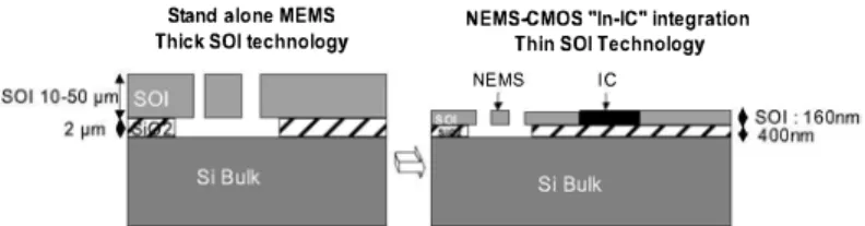
Thin SOI technology is capable to push forward the possibilities by offering the ability to provide horizontal integration directly at the front-end level. Thin SOI technology means thin silicon top layer, for example 160nm thickness if we consider the 0.13µm CMOS SOI technological node. The idea is to use this thin silicon layer, traditionally dedicated to the CMOS process, for the MEMS fabrication (Fig. l ). The first consequence is that at least one dimension of the MEMS structure is shrinked to the nanoscale. As a consequence the mechanical device must be considered as a NEMS (Nano-Electro-Mechanical Systems).
1 CEA/LETI - 17 rue des Martyrs 38054 Grenoble Cedex 9 - France 2 ESRF - B.P. 220, 38043 Grenoble cedex 9 -France
3 CNRS/LEPES, 25 avenue des Martyrs, 38042 Grenoble Cedex 9 -France
Universite Joseph Fourier, B.P. 53, 38041 Grenoble Cedex 9 - France
4 STMicroelectronics - 850 rue Jean Monnet, 38926 Crolles - France
*Corresponding author: Eric Ollier, Tel : 33 4 38 78 57 35, Fax: 33 4 38 78 51 69, e-mail : [email protected]
Stand alone MEMS
Thick SOI technology NEMS.CMOS "In-IC" integration Thin SOI Technology NEMS IC
Figure I. From NIEMS devices to NEMS devices on Thin SOI substrate
Despite the technological difficulties arising, this constrain can also be considered as an opportunity to benefit from the attributes of NEMS. Indeed, NEMS (Nano-Electro-Mechanical-Systems) devices are emerging as a new field with a great deal of interest because they offer in the same time compatibility with "In-IC" integration and also very interesting specific advantages such as potential ultra miniature size elements, low power consumption, potential high resonant frequencies and quality factors, fast response time, high sensitivity to applied force, external damping or additional mass. As a consequence, NEMS are very promising for ultimate sensing, autonomous sensors, battery-operated systems and can allow new architectures. Nowadays, NEMS are investigated in order to face the challenges of nano-world and have a better understanding of the fundamental issues of mechanics in the nano-scale [ 1]. But thanks to the combination of powerful attributes such as unprecedented mass sensitivity and high operational resonance, NEMS opens up the possibility to prospect ultimate inertial mass sensing [2]. Resonant NEMS can also be combined with nanoelectronic [3] to fabricate displacement detectors based on RF-SET (Radio-Frequency Single-Electron Transistor). NEMS-IC integration is highly suitable since it can enable to decrease the cost of MEMS. In addition, good performances can be expected because the proximity between NEMS and IC enables to suppress a lot of parasitic effects. In particular, thin SOI technology is a very good candidate since the same thin layer of single-crystal silicon can be used for both mechanical structures and advanced ICs.
In particular, this approach can be attractive for low cost accelerometers for applications such as: hard-drive protection, motion interface for cell phones, handheld PDAs, game controllers and also gesture recognition or motion capture for medical, wellness or sports activities [ 4].
II. MODELING AND DESIGN
50G and lOG accelerometers have been designed in two configurations: In-Plane (IP) accelerometers with sensitive axis included in the plane of the wafer, and Out-of-Plane (OOP) accelerometers with sensitive axis perpendicular to the wafer (Fig.2). An acceleration causes the motion of a proof-mass and the corresponding displacement is measured by means of a variation of capacitance between two sets of electrodes. The electrodes are either interdigitated combs (IP) or two parallel plates (OOP).
In-Plane (IP) accelerometer Out-of-Plane (OOP) accelerometer
Electrostatic combs
V1 V2
Mechanical springs Mechanical springs
Figure 2. Principle of IP (In-Plane) and OOP (O ut O f Plane) accelerometers
If we consider 0.13µm CMOS SOI technology, the first constrain to take into account is the 160nm thickness of the silicon top layer that will be used for the NEMS and MEMS structures. In order to avoid parasitic deformations and undesirable vibration modes the mass size has been limited to typical dimensions of 75xl5
0
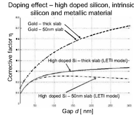
µm and lOOxlOOµm, respectively for IP and OOP accelerometers. As a consequence the mass is about 4ng. In addition, for IP accelerometers, low cross-sensitivity implies to increase the ratio thickness/width of the mechanical springs, leading to 50nm wide mechanical springs. In the same time, increase electrical sensitivity means decrease electrostatic gap down to 100-400nm. Finally, depending on the acceleration range and the resolution expected, the length of mechanical springs and the number of teeth of the electrostatic comb have been adapted. Typically, the length of springs and electrostatic teeth range from 1 to 1 O µm. For OOP accelerometers, the electrostatic gap is fixed by the 400nm BOX thickness. The mechanical springs are typically a few micrometer wide and lOµm to lOOµm long depending on the acceleration range. The mechanical stiffuesses investigated in this study range from 10-2 to 0.3N/m.The resonance frequencies are respectively about 10 to 20KHz for IP and OOP accelerometers. Because of thin SOI technology, some dimensions have been reduced drastically compared to traditional thick SOI technology and are now situated in the nano-scale, in particular the mechanical spring width (50nm) and the electrostatic gaps ( 100-400nm ). As a consequence, the role of specific phenomenon occurring in the nano-scale has been studied, in particular the roleof quantum non-gravitational attraction named Casimir force. This force occurs at intermediate distances, between Van der Waals forces and electrostatic forces and can be attractive or repulsive depending on the conditions. A novel model has been developed for silicon devices in order to take into account doping level and dimensional effects. A corrective factor ri=Fc/Fi is applied in the commonly used formulas established assuming parallel metal plates [5]. Fe is the corrected Casimir force, Fi is the ideal Casimir force assuming two uncharged infinite parallel plates with perfect conductivity. Fig.3 illustrates the effect of doping level and slab thickness on the corrective factor. These simulations show that silicon structures, even highly doped, allow to reduce the impact of Casimir force on the device behaviour compared to the ideal case with electrodes constituted of metal.
Doping effect - high doped silicon, intrinsic silicon and metallic material
Gold - thick slab ·
i
"·"Gold-50nm.slab
·�
·�.��---�----JQ
0-5 . . . ,.��..-:../Cl) .r"""'
:....Cll;
"' · _;./High doped Si-thickislab (LEH model),,
�
0.3 ;"·u "·'
/
--- ---7
--High doped Si -50nm slab (LETI ;,.;bci�i)
Gap d[ nm]
Figure 3. Effect of doping level and slab thickness on Casimir corrective factor
Based on this model, 50G accelerometers have been designed in both IP and OOP configurations. IP50G accelerometers are constituted of a 75µmxl50µm proof mass, electrostatic combs with teeth 80nm wide and gaps 130nm to 400nm wide. With 130nm gap, the mechanical spring is 50nm wide and 4µm long. With 400nm gap, the mechanical springs are 50nm wide and 11 µm long. OOP accelerometers are constituted of a lOOµmxlOOµm proof mass with an electrostatic gap 400nm wide. The mechanical springs are lOµm wide and 80µm long.
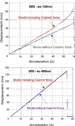
It has been demonstrated that the architecture has a strong influence on the impact of Casimir force. In particular, relative large gap and small tooth width minimize Casimir effect. As a consequence, a trade-off must be found between high sensitivity and low Casimir effect. Indeed, to reach better sensitivity, the flexure stiffuess and/or the gap between two adjacent teeth must be decreased, but, in that case, Casimir impact tends to reduce the pull-in voltage, increase the capacitance variation and induce larger non-linearity. Fig.4 shows displacement/acceleration curves including the effect of Casimir force for IP-50G accelerometers, respectively for 130nm and 400nm gaps. This figure illustrates that for IP accelerometers, large gap ( 400nm) ensures negligible influence of Casimir force, but for smaller gaps (130nm), the impacts have quickly to be considered.
60 ---T---,- -1-- --1---- 1-- - -T 1 50G-eo130nm 1 1 E 50
---f---�
----:----:---y
�
--
j
�
S 40 ___ �()d_e�in,c�u�in.g_s_a_si�i_r!o_r:c!'l _ 1 ___�
C I I I �I I l Q) I I I 14 /,.. I ,,...,,. ... ·I E 30 - - - - L - - - l_ - - - _J -- - -!--'"' --?'..,--'-- - L � I I�l
•. • II
I
C'OI
I I /-<'" I !�
20---t ---�
::.�::-�.-"'_,,.
-� ---�
---t
(5 i ... -)...-··"' I:\
It
.
10---;z�� -Model without Casimir force
/1 .... I 0 10 20 30 40 50 Acceleration (q) 140 ---,---, ---, ----� i 50G - eo 400nm , 1 120 - - - - L - - - L - - - L - -- 1--- i I I I I
f
100 _ .M()d_e�iric�ud_i�g_C_ai;i�i�f()rc;e ___ � __ _�
80 ----�
---:
�
--:----:--
1
--� ! II
I
i
60----:
---�- \--:---:---0 40 �-�o:� :i;h�Lrt ;a���r �o�c:--
1
-20--- !- - 1 I
---60
10 20 30 40 50 60
Acceleration (g)
Figure 4. Displacement/acceleration curves for IP 50G accelerometer with respectively J 30nm and 400nm gap (Influence of Casimir Force)
Fig.5 and 6 give expected mechanical and electrical performances respectively for IP-50G and OOP-50G accelerometers.
Mechanical results Mechanical results
Weiqth (Kq) 4,10E-12 Weigth (Kg) 4,10E-12
Stiffness (uN/um) 0,07 Stiffness (uN/um) 0,017
Mechanical sensitivity (nm/g) 1 Mechanical sensitivity (nm/g) 2,4
Electrical results Electrical results
Pull-in voltaae !mVl 220 Pull-in voltaqe (V) 1,45
Pull-in displacement (nm) 52 Pull-in displacement (nm) 133
Co (fF) 7,3 Co (fF) 0,89
C full range (50G) (fF) 3,25 C full ranqe (50G) (fF) 0,4 Electrical sensitivity (aF/g) 60 Electrical sensitivity (aF/g) 8 Figure 5. Expected performances of IP 50G accelerometers (130nm- 400nm gap)
Mechanical results
Weiath !Ka) 3,64E-12
Stiffness (uN/um) 0,017 Mechanical sensitivity (nm/g) 2,6 Electrical results Pull-in voltaae (mV) 110 Pull-in disolacement (nm) 110 Co (fF) 55,3 ° C full ranqe (50G) (fF) 28
Electrical sensitivity (aF/g) 540
Figure 6. Expected performances ofOOP 50G accelerometers (400nm gap)
IP accelerometers exhibit pull-in voltage from a few lOOmV to l.5V respectively for 130nm and 400nm gap width. FS
capacitance change is 3.5fF down to 0.4fF respectively for 130nm and 400nm gap width. OOP accelerometers exhibit driving voltage about a few 1 Om V to 1 OOmv and FS capacitance change around a few lOfF. The sensitivities are respectively in the ranges of 10-lOOaF/g and 500-lOOOaF/g for IP and OOP accelerometers. These figures are far from conventional MEMS but can be considered as acceptable considering the fact that ultra low noise CMOS ICs are capable to resolve better than laF/sqrt(Hz) of capacitance variation. Moreover NEMS structures developed with "In-IC" integration approach will benefit of reduced parasitic capacitances allowing to expect to resolve 10-3aF/sqrt(Hz) .
Ill. THIN SOI FABRICATION
The fabrication of NEMS devices and accelerometers (Fig. 7) is based on Thin SOI 130nm technology and 200mm facilities. The Si top layer is 160nm thick and the BOX oxide is 400nm thick.
Electrostatic
Beam corrb Sisnic rrass Contact pads
Thin SOI Substrate Si top layer 160nm Oxide 400nm Doping electrical parts Implantations (Si top, Si bulk) Patterning NEMS, MEMS Hybride lithography
(E-beam + DUV)
Etching NEMS, MEMS RIE etching Si top
Metal deposition Metal deposition and etching
Release NEMS-MEMS FH-vapor release
Figure 7. Simplified flow-chart for fabrication of thin SO I NEMS
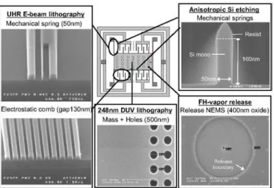
Scaling considerations have been addressed in order to realize on the same wafer the nano-structures (springs, electrostatic combs) and the large structures (proof mass, electrical pads . . . ). To reach this goal, hybrid lithography combining advanced UHR e-beam and 248nm DUV lithographies has been used. In addition, FH-vapor technique has been improved to enable the release and protection against sticking despite the 500nm diameter of the release holes and the 400nm thickness of the sacrificial oxide. Finally, AlSi metal was used for electrical pads.
These technologies have allowed to manufacture different NEMS structures such as thin mechanical beams, large mechanical structures like membranes of rigid masses and also narrow gaps
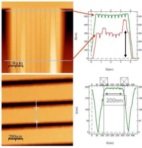
for electrical purposes. Fig. 8 illustrates how these technologies are used and highlights a few results obtained. In particular, mechanical beams 50nm wide and electrostatic gaps 100-400nm wide have been manufactured (Fig. 9).
Figure 8. Technology developments for fabrication of NEMS & accelerometers
Figure 9. Elementary NEMS structures :thin mechanical beams and narrow gaps
After release, the static behaviour of these N-MEMS structures depends strongly on the design. The potential defaults, illustrated on Fig. 10, are substrate or lateral sticking and residual deflections due to stresses. Nevertheless, appropriate design is capable to limit this kind of problems. Lateral and vertical stiffuesses must be sufficient to avoid sticking problems. Limitation of large structures dimensions and flexible beams length allows to limit residual deflections.
Figure I 0. Examples of potential defaults encountered with NEMS structures
These technologies have been used to manufacture thin SOI 50G IP and 50G OOP accelerometers (Fig. 11 & 12). Fig. 13 presents SEM photograph of a thin SOI IP NEMS accelerometer.
Figure 11. Photograph of thin SOI NEMS IP50G accelerometer
Figure 12. Photograph of thin SOI NEMS OOP50G accelerometer
Figure 13. SEM photograph of thin SO I NEMS IP accelerometer
IV. CHARACTERIZATION
Characterization of devices including NEMS structures is really challenging because some dimensions are in the nano-scale. In
addition, the structures are free standing and sometimes exhibit low stiffuess. AFM technique has been investigated in order to provide measurement related to released NEMS structures. Specific procedures have been developed to solve the problems encountered, in particular to avoid breaking or instability occurring in case of low stiffuess structures. AFM is used in tapping mode. This mode allows to limit mechanical interaction between the AFM tip and the NEMS measured. The oscillations are damped due to interaction between AFM tip and the surface in particular by Van der Waals forces. The cantilever is excited at resonance frequency
(
50-300kHz)
with an amplitude of a few 1 Onm and a control of the oscillation amplitude. The AFM tip must be chosen carefully by considering mechanical stiffness, resonance frequency, curvature radius. In addition imaging conditions must be optimized for NEMS measurement. In particular, the amplitude set point is fixed to ensure soft tapping, the scan rate is reduced to ensure low scanning speed and the Zlimit is fixed to ensure maximum vertical resolution. Vertical resolution is excellent
(
about A)
. Lateral resolution is limited by tip radius of curvature(
a few nm)
. This AFM technique is now capable to provide information such as substrate/lateral sticking(
Fig. 14). measurement of critical dimensions like cantilever beam vertical deflection and width(
Fig. 15)
, with atomic resolution for vertical axis and a few nm for lateral resolution. These techniques have been used to investigate and characterize the behaviour of fabricated thin SOI IP and OOP accelerometers. In particular vertical position of the mechanical structure after release process has been investigated in details. Fig. 16 and 1 7 show characterization results related to vertical residual deflections of free-standing IP50G and OOP50G accelerometers after the end of the process.Fixed part Movable Fixed part
• N / Fixed part -0 N ., »
�--0 � ,.3 nm iil t\�
g
» g· » Fixed part '"' » Movable '"' 420 nm l> .. NEMS )> » Movable TI " ;::: � s: NEMS . -o·I
a·i
i
.AFM tip displacement (nm) AFM tip displacement (nm) Figure 14. AFM images and measurement of relative vertical position of fixed and
released structures, for sticking problem evaluation
Figure 15. AFM characterization of first NEMS structures Cantilever beams: Thickness160nm - Width 200 nm -Length 1-few10µm
IP-SOG
Az= 0 nm Az= -4 nm
Az= 0 nm
Figure 16. AFM characterization of IP 50G accelerometer L1z: vertical misalignment of movable structure
Az= -4nm
Az= +2nm
Figure 17. AFM characterization ofOOP 50G accelerometer L1z: vertical misalignment of movable structure
Figure 18 presents results of AFM measurements concerning vertical position of NEMS structures after release process for 50G IP and OOP accelerometers.
Type of Characteristics Residual vertical accelerometer deflection (nm) In-Plane Electrostatic Gap I 50nm < +/- 6 nm 50G Mass 75x75µm
Electrostatic Gap 130nm <+/- II nm Mass 75xl 50µm
Out-of-Plane Electrostatic Gap 400nm < +/- 6nm 50G Mass IOOxl OOµm
Figure 18. "Static characterization" of thin SOI IP50G and OOP50G accelerometers : vertical residual deflection after release process
These results show that appropriate design and technology allow to fabricate IP-50G and OOP-50G thin SOI accelerometers exhibiting negligible vertical residual deflection after process compared to the l 60nm thickness.
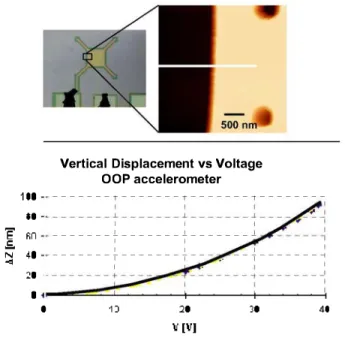
In addition, "electro-mechanical" behaviour of NEMS submitted to driving voltage has been investigated. A line including a fixed part and a movable part is selected. Then images are realized for different actuation voltages. The main difficulty comes from the fact that AFM measurement is influenced by the electrical field created near the beam tip when a voltage is applied between different parts of the NEMS device.
Fig. 19 shows the first AFM characterization of displacement versus applied voltage obtained on a OOP 50G accelerometer submitted to an electrostatic force.
100 60 � fin .E. N .... 40 w 0 0
Vertical Displacement vs Voltage OOP accelerometer ---1---1---1 ---I I I _______ L _______ �---� I I I I I 1 _______ T _______ T ___ • --T--- � I I 1) 20 \l[\I) 30 40
Figure 19. First result of"electro-mechanical characterization" of Thin SOI OOP 50G accelerometer
The deflection obtained under applied voltage is 90nm ( 400nm gap). This first result demonstrates the capability of AFM technique to provide characterizations of electro-mechanical behaviour of NEMS devices and shows the feasibility of electrostatic driving of our NEMS structures. This work is still on progress in order to improve the AFM measurement and have a better understanding of NEMS electro-mechanical behaviour.
V. CONCLUSION
First Thin SOI NEMS structures for accelerometers compatible with "In-IC" integration have been designed and fabricated in a thin 160nm SOI layer in order to be compatible with 0.13µm CMOS SOI technology. IP and OOP configurations have been designed and fabricated. The modeling and design take into account specific phenomenon occurring in the nano-scale, in particular Casimir force. NEMS accelerometers with mechanical springs 50nm wide, electrostatic gaps 130-400nm wide have been fabricated thanks to the use of hybrid lithography combining e-beam and DUV lithography and also FH-vapor release to limit sticking problems. AFM techniques have been investigated and optimized to characterize NEMS structures and accelerometers. It has been shown that appropriate design and technology enable to fabricate devices exhibiting negligible residual deflections and good mechanical behaviour after process. In addition, AFM has been investigated for electromechanical characterizations of NEMS and accelerometers submitted to an actuation voltage. The deflection obtained with OOP accelerometers demonstrates the capability of AFM technique to provide this kind of characterizations and also the feasibility of electrostatic driving of our NEMS structures. Complementary characterizations are currently on progress in order to characterize electro-mechanical static and dynamic behaviour and also to investigate more m
details limitations in performances.
ACKNOWLEDGMENT
Author acknowledges the support of European Commission
for the funding of the integrated Project MIMOSA
IST-2002-507045
REFERENCES
[I] M.L. Roukes, "Nanoelectromechanical systems", Solid State Sensor and Actuator Workshop, Proceedings pp. 529-551, South Carolina, June 4-8, 2000
[2] K.L. Ekinci, Y.T. Yang, M.L. Roukes, "Ultimate limits to inertial mass sensing based upon nanoelectromechanical systems", Journal of Applied Physics, V95, N°5, pp. 2685-2689, March 2004
[3] J.D. Aldridge et al, "Nanoelectronic and nanomechanical systems", SPIE Proceedins 4591, 11, 200 I
[ 4] http://www.mimosa-fp6.com
[5] P. Andreucci, L. Duraffourg, E. Oilier, V. Nguyen, M. T. Delaye, P. Robert, "Impact of Casimir force on nano accelerometers modeling", IEEE Sensors