HAL Id: tel-01773745
https://tel.archives-ouvertes.fr/tel-01773745
Submitted on 23 Apr 2018HAL is a multi-disciplinary open access archive for the deposit and dissemination of sci-entific research documents, whether they are pub-lished or not. The documents may come from teaching and research institutions in France or
L’archive ouverte pluridisciplinaire HAL, est destinée au dépôt et à la diffusion de documents scientifiques de niveau recherche, publiés ou non, émanant des établissements d’enseignement et de recherche français ou étrangers, des laboratoires
aging effects
Mauricio Altieri Scarpato
To cite this version:
Mauricio Altieri Scarpato. Digital circuit performance estimation under PVT and aging effects. Micro and nanotechnologies/Microelectronics. Université Grenoble Alpes, 2017. English. �NNT : 2017GREAT093�. �tel-01773745�
Pour obtenir le grade de
DOCTEUR DE LA COMMUNAUTE UNIVERSITE
GRENOBLE ALPES
Spécialité : Nano Electronique et Nano Technologies
Arrêté ministériel : 25 mai 2016
Présentée par
Mauricio ALTIERI SCARPATO
Thèse dirigée par Édith BEIGNÉ, HDR, CEA-LETI, et codirigée par Suzanne LESECQ, HDR, CEA-LETI préparée au sein du Laboratoire d’Electronique et des Technologies de l’Information, CEA Grenoble
dans l'École Doctorale Electronique, Electrotechnique, Automatique et Traitement du Signal (EEATS)
Estimation de la performance
des circuits numériques sous
variations PVT et vieillissement
Thèse soutenue publiquement le 12 décembre 2017, devant le jury composé de :
Mme. Lorena ANGHEL
Grenoble INP, PrésidenteM.
Daniel MENARD
INSA Rennes, RapporteurM.
Abdoulaye GAMATIE
LIRMM, RapporteurM.
Olivier HÉRON
CEA-LIST, ExaminateurMme. Édith BEIGNÉ
CEA-LETI, Directeur de thèse, Invitée
Mme. Suzanne LESECQ
It is my pleasure to acknowledge the roles of several individuals who were funda-mental for completion of my PhD thesis.
Firstly, I would like to express my gratitude to Abdoulaye Gamati´e and Daniel M´enard for reviewing my manuscript and giving me important feedbacks. My sincere thanks also to Lorena Anghel, whom I had the pleasure of having as teacher at ENSIMAG, for accepting the invitation to chair my thesis defense.
I am highly indebted and thoroughly grateful to my supervisors Edith Beign´e, Olivier H´eron and Suzanne Lesecq who encouraged and directed me through these three years. This thesis would not come to existence without their guidance and large background in different specialties. More than anything, it was their strong support and confidence on me that kept me up during the moments of uncertainty of the thesis.
I am grateful to all my colleagues from both LIALP and LISAN laboratories. Having such amazing work environment was essential for succeeding in my PhD. I must confess that the almost daily croissants/cakes in the cafeteria were an extra motivation to get to the lab every morning. I especially mention Adja Sylla and Thierno Barry who shared with me this hard but rewarding experience of doing a PhD. I am thankful to Vincent Olive, head of LIALP, as well as to Fabien Clermidy and J´erˆome Martin, former and current heads of LISAN, for providing me with all meanings I needed to make the most of my time as PhD student at CEA.
I am also deeply thankful to Ivan Miro-Panades who shared with me his vast knowledge on digital monitors and circuit reliability. Thanks to David Coriat for providing me the netlists from the FRISBEE circuit. Thanks to Anca Molnos for helping me with learning methods. Thanks to Diego Puschini for having mentored me in various subjects since my internship and for bringing mate to the lab. Thanks to Marc Belleville and Pascal Vivet for their advices. Thanks to Chiara Sandionigi as well as to all LCE co-workers who I had the pleasure to meet in Saclay. I had a short but enriching stay there. Finally, thanks to everyone who helped me directly or indirectly during my PhD, it would not be
I met in Grenoble. They all make this long journey considerable easier by sharing unforgettable moments with me. A special thanks to my roommates Arthur and Joo Paulo for making our coloc the best one in Grenoble. I want to extend my thanks to Fernanda Kastensmidt and Jos´e Rodrigo Azambuja for introducing myself to the research environment at UFRGS.
Lastly but most importantly, I want to thank my family for all support they gave me despite the distance. My family have always been my base of support, even more so after I came to France. They always encouraged me to pursue my dreams even though it meant that I would be far away from them. Most of all, I dedicated this thesis and all my achievements to my mother who made my happiness the priority of her life since I was born. Obrigado m˜ae, te amo muito!
Contents iii
List of Acronyms vii
Introduction ix
Context . . . ix
Motivations and Objective . . . xi
Contributions . . . xii
Report Organization . . . xiv
1 Sources of variability in advanced technology nodes 1 1.1 Process variations . . . 2
1.1.1 Global process variations . . . 2
1.1.2 Local process variations . . . 3
1.2 Supply voltage variations . . . 5
1.3 Temperature variations . . . 7
1.4 Aging effects . . . 9
1.4.1 Negative/Positive Bias Temperature Instability (N/PBTI) and Hot Carrier Injection (HCI) . . . 9
1.4.2 Destructive aging effects . . . 10
1.5 Conclusion . . . 11
2 Techniques for coping with variability in digital circuits 13 2.1 Introduction . . . 14
2.2 Adaptive architectures . . . 17
2.2.1 Adaptation strategies . . . 18
2.3 Monitoring systems . . . 21
2.3.1 Timing fault detection and fM AX tracking . . . 22
2.3.2 Process, voltage, temperature and aging monitors . . . 28
2.4.1 Multiprobe: an all-digital on-chip sensor to monitor VT
variations . . . 33
2.4.2 Impact of BTI and HCI effects on measurements . . . 36
2.4.3 Aging-aware recalibration proposal . . . 40
2.5 Conclusion . . . 43
3 Performance estimation under PVT and aging variations: a circuit-level methodology 45 3.1 Objective . . . 47
3.2 Overview of the proposed methodology . . . 48
3.2.1 First stage: Delay Modelling . . . 48
3.2.2 Second stage: Aging Modelling . . . 49
3.3 Experimental set-up and SPICE reliability simulation . . . 50
3.3.1 Benchmark circuit . . . 50
3.3.2 Device-level aging simulation . . . 51
3.4 Application of the first stage of the proposed methodology: Delay modelling . . . 53
3.4.1 Choice of the Delay model formula . . . 53
3.4.2 Estimation of the Delay model formula parameters for the path under study . . . 54
3.4.3 Analysis of the process variation on the delay estimation . . 57
3.5 Application of the second stage of the proposed methodology: Ag-ing modellAg-ing . . . 59
3.5.1 Shift of Delay model parameter(s) due to aging . . . 60
3.5.2 Construction of the ∆pVth model formula . . . 62
3.5.3 Example of ∆pVth model parameters . . . 68
3.5.4 Impact of workload on aging . . . 71
3.5.5 Correlation of aging with process variations . . . 73
3.5.6 Considerations regarding dynamic variations . . . 74
3.6 Validation of the complete model . . . 78
3.6.1 Validation in another benchmark circuit . . . 80
3.7 Conclusion . . . 82
4 Integration of circuit-level models in different application con-texts 85 4.1 Related works on circuit-level aging modelling . . . 87
4.2 On-line estimation of circuit degradation . . . 88
4.2.1 Control loop for Adaptive Voltage and Frequency Scaling . 88 4.2.2 Dynamic Mean Time to Failure (MTTF) computation . . . 91
4.2.3 Maximum operating conditions . . . 92
4.2.4 Simplified on-line estimations . . . 93
4.3.1 Description of the multi-core simulation framework . . . 95 4.3.2 Task mapping strategies: Performance × Energy ×
Relia-bility trade-off . . . 98 4.4 Simulation of an Adaptive Frequency Scaling (AFS) system under
aging variations . . . 101 4.4.1 Complete AFS system model in Simulink . . . 101 4.4.2 Aging degradation measurement for an AFS system . . . . 103 4.5 Conclusion . . . 107
5 Conclusion and Perspectives 109
5.1 Synthesis . . . 109 5.2 Perspectives . . . 112 Bibliography 115 List of Publications 129 International Journals . . . 129 International Conferences . . . 129 Patents . . . 130 List of Figures 131 List of Tables 136
ABB Adaptive Body Bias . . . 20
ADC Analog-to-Digital Converter . . . 29
AFS Adaptive Frequency Scaling . . . v
AVFS Adaptive Voltage and Frequency Scaling . . . 17
AVS Adaptive Voltage Scaling . . . 18
BTI Bias Temperature Instability . . . 1
CPR Critical Path Replica . . . 23
DVFS Dynamic Voltage and Frequency Scaling . . . 17
EDA Electronic Design Automation . . . 16
FIT Failure in Time . . . xi
FLL Frequency-Locked Loop . . . 19
HCI Hot Carrier Injection . . . 1
LUT Look-Up Table . . . 90
PLL Phase-Locked Loop . . . 19
PVT Process, Voltage and Temperature . . . 1
PWM Pulse Width Modulator . . . 18
RISC Reduced Instruction Set Computer . . . 80
SSTA Statistical Static Timing Analysis. . . .16
STA Static Timing Analysis . . . 16
UTBB FD-SOI Ultra-Thin Body and Box Fully-Depleted Silicon-On-Insulator . . . 21
VCO Voltage-controlled oscillator . . . 19
Vbb Body bias voltage . . . 20
Vdd Supply voltage. . . .x
“With engineering, I view this year’s failure as next year’s opportunity to try it again. Failures are not something to be avoided.
You want to have them happen as quickly as you can so you can make progress rapidly.”
Gordon Earle Moore, Intel co-founder and author of Moore’s law.
Context
In 1965, Gordon Moore forecast that the number of transistors in an integrated circuit would double every two years [1], which has since become widely known as Moore’s Law. The continuous increase in transistor density has lead to huge increases both in performance and in the number of functionalities per circuit. In turn, this has boosted the development of mobile applications like laptops, tablets and mobile phones. Besides calling and texting, current mobile phones incorporate additional features like browsing, playing games, taking pictures, etc... Moreover, a phone nowadays has the same processing performance than a high-end desktop computer had ten years ago.
Due to physical limitations (weight and size), the battery capacity of such devices cannot be expanded at the same rate as their performance. For instance, the Samsung Galaxy S5 phone, launched in 2014, had a battery capacity of 2800 mAh. Three years later, the Samsung Galaxy S8 phone was launched with a battery of 3000 mAh. This corresponds to an increase of only 7% in battery capacity while the processing performance has increased about 300% [2]. More than the performance, it is therefore the energy efficiency that must be improved, also known as performance per watt. Otherwise, the battery would not be able to afford such processing power.
Improvements on energy efficiency are mandatory not only for mobile appli-cations. The concept of Internet of Things (IoT) has become popular in the last years. It corresponds to devices that interoperate through network connectivity. This leads to new application domains, for instance smart house, healthcare, de-fense, industry automation and transport network, where the interconnection of
theses devices provide new services to the end-users. Intel has estimated that 2 billion devices were connected by 2006 while this number raised to 15 billions by 2015. At that pace, they expect 200 billions connected objects by 2020 [3]. With such an escalation in the number of connected devices, it is no wonder that their energy consumption has become a major issue. Indeed, a report issued in 2015 by the Semiconductor Industry Association (SIA) stated that the computer devices will require more energy than the world can generate by 2040 [4].
Since both dynamic and leakage power depend on the Supply voltage (Vdd), the main approach to reduce energy consumption so far consisted in scaling down Vdd with transistor size. However, the reduced transistor dimensions has exacer-bated the impact of variability on CMOS circuits. The sources of variability can be either static (due to manufacturing imperfections - P variability) or dynamic (due to Vdd and temperature fluctuations - VT variability). Therefore, deep submicron technologies require the use of large voltage guard-bands to ensure a ”correct” operation of the circuit under these different sources of variability, the objective being to have a functional circuit even in the presence of PVT variabil-ity. This has lead to a slowdown of Vdd scaling in recent technology nodes, as shown in Figure 1 [5].
Figure 1: Energy and Vdd scaling vs. technology node [5].
Considerable energy savings can be achieved by decreasing these safety mar-gins. This is done through the use of an adaptive management scheme. Such techniques use embedded sensors that track the fluctuation of the circuit tim-ing induced by static and dynamic variations. Then, a variable voltage actuator and/or clock frequency actuator (and possibly a body bias actuator) changes on the fly the operating conditions of the circuit to reduce its energy consumption while avoiding timing faults. Vdd is kept at its minimum functional value or, respectively, the clock frequency is kept at its maximum value. The main limita-tion of current adaptive techniques is that they do not distinguish the source of
the variation while they detect the variation of the circuit timing. In advanced technology nodes, aging has become an important source of variability, in par-ticular BTI and HCI effects. Unlike other dynamic variations, the aging-induced shift of the circuit performance is permanent. It can thus lead the circuit to an irreversible unreliable condition.
Aging might not be a real problem for customer electronics, because their life span is smaller than 10 years and they usually do not operate at harsh environ-ments. Nevertheless, it is a major issue for safety-critical real-time systems, such as aerospace and automotive ones. These systems demand high performance with very low failure rate. For example, avionics systems require over 25 years of oper-ation with a maximum failure rate of 100 Failure in Time (FIT) [6], where 1 FIT corresponds to 1 failure per billion hours. Moreover, they are used in extreme conditions, where the temperature can range from -50◦C to 150◦C. The mission profiles of such critical systems are highly diversified making it impossible to ac-curately estimate the aging degradation during the design phase. The worst-case scenario approach is thus taken into account to fulfill the performance and safety requirements. However, this leads to an excessive energy consumption due to the pessimistic voltage guard-bands.
Motivations and Objective
Aging of human beings is determined by the way we live, i.e. how healthy we eat, how much sport we do, etc... This is also valid for an electronic circuit whose aging does not depend only on its age. Two identical circuits with the same age do not necessarily present the same aging degradation. The degradation depends on how the circuit was used during its lifetime, i.e. the historic of its operating conditions, namely, supply voltage, temperature and workload. This is why the estimation of circuit aging is not simple. Moreover, the impact of aging on the circuit performance is governed by the operating condition once the degradation of the transistor characteristics causes a shift in the propagation delay that depends on the PVT conditions. For instance, while a transistor degrades faster at a higher supply voltage, an aged transistor has a higher relative influence on the circuit performance when it operates at a lower supply voltage.
In the last years, many works have focused on modelling aging effects in transistors, particularly BTI and HCI. Such works managed to provide accurate models for the aging-induced shift of transistor characteristics, especially the threshold voltage. These models are based on the physical mechanisms of aging and they are validated on silicon data for several combinations of voltage and temperature values. Such models can be integrated in electronic circuit simula-tors, e.g. SPICE, which allows the assessment of the circuit degradation for any operating condition. However, as stated above, the mission profile of a circuit is
barely known at the design phase. The use of existing aging models is thus not enough for estimating the circuit degradation, whatever their accuracy is.
Having an on-line estimation of the circuit health would allow to calculate on the fly the required safety guard-bands. Besides, it could be used by relia-bility strategies to improve the circuit lifetime. However, an integrated circuit nowadays is composed of millions or billions of transistors. Even a single crit-ical path comprises more than a hundred transistors. Applying transistor-level models to on-line estimate the circuit degradation is computationally impractical. AS a consequence, simplified models must be adopted so that the computation overhead is not larger than the benefits provided by its use.
The objective of this PhD thesis is to propose a methodology to abstract the complexity of existing aging models. The idea is basically to generate circuit-level aging models for synchronous digital circuits. Such models are simple equations that provides the propagation delay of a critical path considering PVT variations together wigh aging. The historical values of PVT are taken into account to estimate the aging degradation. Instead of estimating the Vth shift for each
transistor, the proposed models estimate an overall parameter shift for the whole path. Being architecture- and technology-independent, this methodology can be applied to any digital circuit.
Contributions
The main contributions of this work are:
• Propose a methodology to generate a circuit-level aging model from device-level models
A methodology is proposed to model the propagation delay of a critical path from device-level models. The resulting model gives the critical path delay based on the PVT conditions. The parameters of the model are obtained through non-linear regression from data obtained with SPICE simulations. From the propagation delay model, a second model for both BTI and HCI effects is proposed. The model reflects the aging-induced propagation de-lay shift for any PVT condition. In other words, it is integrated in the delay model as a parameter shift. This latter model takes into account all factors that influence the aging degradation, namely, supply voltage, tem-perature, workload and circuit topology. Dynamic variations are also taken into account to allow on-line estimation.
This contribution has been published in “Towards on-line estimation of aging in digital circuits through circuit-level models”, IRPS’17 [7]. A patent application, “Method and device for estimating circuit aging” [8], has also been filed.
• Develop an aging-aware solution to estimate voltage and temper-ature variations
Many sensor solutions exist in the literature to track voltage and temper-ature changes. However, none had directly addressed the impact of aging effects on its operation so far, although some works assume that their ar-chitecture is robust to aging. Moreover, an aging-aware VT sensor must be adopted to allow the use of the proposed circuit-level models to on-line estimate the circuit health.
Therefore, we first analyzes the impact of both BTI and HCI effects on the voltage and temperature estimates provided by a small area digital sensor. Then, we proposed a recalibration method that increases the sensor robustness against aging effects.
This work has been presented in the publication “Evaluation and mitiga-tion of aging effects on a digital on-chip voltage and temperature sensor”, PATMOS’15 [9].
• Demonstrate the application of the proposed models in different contexts
The circuit-level models proposed in this thesis can be used either on-line to estimate the circuit health or off-line to simulate the operation of the circuit under aging effects. We shortly discuss four possible on-line appli-cations of the proposed models. The proposed appliappli-cations consist in an adaptive control, a dynamic Mean Time To Failure (MTTF) computation, an estimation of the maximum operating conditions for a given MTTF and a reliability measure for task mapping in multi-core circuits. Then, the models are used in two off-line modelling contexts:
- the first one is a framework to simulate a multi-core circuit. This frame-work allows the implementation of strategies of task mapping and DVFS. Different strategies are implemented and evaluated here with respect to aging, performance and energy consumption;
- the second is an adaptive system implemented as a Simulink model. This circuit constantly changes its clock frequency based on embedded sensors that are placed at the critical paths and warns the pre-occurrence of a timing fault. From the simulations, a technique is proposed to estimate the aging-induced performance shift of such systems by only tracking temperature variations.
The latter contribution is presented in the publication “Tracking BTI and HCI effects at circuit-level in adaptive systems.”, NEWCAS’16 [10].
Report Organization
Apart from this introduction, the report is composed of four chapters and a con-clusion. Chapter 1 introduces the sources of variability in advanced CMOS nodes and their impact on digital circuits. Firstly, it presents the process variations due to manufacturing and atomistic limitations. These variations lead to different val-ues of performance and power than those estimated at the design phase. Next, the dynamic variations are addressed. Local variations of voltage and temperature depend on the circuit operation and they have a strong impact on the switching speed of the transistors. Finally, aging-induced variations are presented. Aging has become a major issue in recent technology nodes, in particular BTI and HCI effects. These phenomena cause parametric shifts in transistors which may result in a faulty operation of the circuit. This chapter exposes then the importance and need for correct modelling of variability as well as adaptive techniques.
Chapter 2 firstly explains how the variability is estimated during the design phase of a circuit and why the traditional approach of safety guard-banding is not anymore suitable. Then, it introduces the concept of adaptive circuit which is basically a circuit that implements an adaptation strategy based on a monitoring system. The adaptation strategy consists in changing the operating conditions of the circuit to cope with variability. This adaptation can be done through the supply voltage and/or the clock frequency. Next, this chapter highlights some existing monitors to track variability. The presented solutions range from timing fault detection to direct measure of the variation. It is shown that current solutions are not able to provide an accurate information about the aging-induced performance degradation. Finally, this chapter addresses the impact of aging on the voltage and temperature estimation with a digital sensor. A recalibration method is proposed to mitigate the aging effects on the voltage and temperature estimates.
Chapter 3 presents the main contribution of this work. It consists in a method-ology to construct circuit-level aging models from device-level models. Based on SPICE simulations, a first model is generated for the propagation delay of a critical path. The resulting model is an equation that depends on the Process-Voltage-Temperature variability. Next, both BTI and HCI effects are modelled as a shift in the parameters of the previous equation. The proposed model takes into account all factors that impact aging, namely, circuit topology, supply volt-age, temperature and workload. The proposed methodology is validated on two different architectures implemented in 28nm FD-SOI technology.
Chapter 4 demonstrates the use of the proposed models in different contexts. First, four on-line applications are shortly discussed. The applications range from the integration in an adaptive system to a dynamic Mean Time to Failure computation. Then, the models are used for a multi-core simulation framework. This framework allows the evaluation of different task mapping strategies with
respect to reliability, power and performance. In the end, the operation of a complete AFS system is modelled in Simulink with the help of the proposed models. As a result, a simplified method is developed to estimate the circuit degradation by tracking both the clock frequency and the temperature variations over time.
Finally, Chapter 5 summarizes the main contributions and proposes future work directions.
Sources of variability in advanced
technology nodes
The continuous shrinking of transistor size leads to great advances in circuit per-formance besides reducing energy consumption and transistor cost. However, this aggressive scaling also makes the CMOS circuits more susceptible to vari-ability. There exist 3 main sources of variability, namely, Process, Voltage and Temperature (PVT) variations. Process variations are due to the mismatch of the manufacturing process. Voltage variations are mostly due to the parasitic impedance while temperature variations are caused by the power dissipated by the circuit. PVT variations change the transistor switching speed and leakage current. These variations may uniformly impact the whole circuit (i.e. global variations) or impact each part of the circuit in a different way (i.e. local varia-tions).
Furthermore, aging effects emerged as a new source of variability in recent technology nodes. Both Bias Temperature Instability (BTI) and Hot Carrier In-jection (HCI) effects degrade the circuit performance by increasing the transistor threshold voltage over time. All this increase of variability is transforming the circuit design in a probabilistic problem instead of a deterministic one. Large safety guard-bands are thus necessary to guarantee a correct operation under the worst-case conditions. In this chapter, we summarize the origin of each source of variability and its impact on digital CMOS circuits.
This chapter is organized as follows. Section 1.1 describes the sources of pro-cess variations at both global and local hierarchical level as well as their conse-quences for digital circuits. Next, Section 1.2 and Section 1.3 present the dynamic environmental variations, namely, supply voltage and temperature, respectively. Finally, Section 1.4 talks about aging effects, in particular BTI and HCI.
1.1
Process variations
Process-induced variations have always been a key concern in integrated circuit design. Process variations imply in the mismatch of transistors characteristics from nominal values. This leads to values of propagation delay and current leakage different from those estimated during the design phase resulting in yield loss. Historically, process variations were mainly due to manufacturing process imperfections. But, as the transistor size approaches the atomic scale, variations due to the intrinsic atomistic nature become more important.
Two types of process variability exist, namely systematic variations and ran-dom variations. Systematic variations are deterministic and repeatable devia-tions that depend on the spatial position of the transistor on the wafer and on its surrounding layout. Systematic effects are mainly due to photolithography limitations. Deep ultra-violet laser with 193nm wavelength is still the main light source used in semiconductor lithography even though technology nodes as small as 10nm are already in manufacturing. Variations due to sub-wavelength lithog-raphy occur from the correlation between adjacent structures, such as lithoglithog-raphy proximity effects (LPE) and well proximity effects (WPE). Since these effects fol-low a clear pattern and are layout-dependent, they can be modeled, predicted and even corrected through resolution enhancement technologies (RETs) such as optical proximity correction (OPC) and phase shift mask (PSM) [11].
On the other hand, random variations are a stochastic phenomenon without clear patterns. Random variations are mainly due to atomistic limitations and they have become the dominant source of process variation as the transistor size scaled below 90nm. Some types of random variations are random dopant fluctuation (RDF), line edge roughness (LER) and gate thickness fluctuation (OTF) [12]. As it is not possible to predict these variations, they require a different statistical treatment. Typically, random variations are characterized and modeled as a Gaussian distribution. Circuits are then designed to reach a given yield considering this probability function. Note that higher the yield desired, higher the safety margins needed.
1.1.1 Global process variations
Besides systematic and random natures, process variations are also classified be-tween global and local. Global variability corresponds to deviations of physical parameters from nominal values with the same change for every transistor on a die. These parameters include channel length (L), channel width (W), layer thickness, resistivity, doping density and body effect [12]. As a consequence, identically designed circuits may have different performances and power charac-teristics. As shown in Figure 1.1 [13], the performance difference between dies within a wafer can be up to 30% while the leakage current can vary up to a factor
Figure 1.1: Frequency and leakage current distribution between dies within a wafer fabricated in 180nm CMOS technology[13].
of 20.
Global variations can be separated in lot-to-lot (L2L), wafer-to-wafer (W2W) and die-to-die (D2D). A lot usually contains 25 wafers, while a wafer may contain hundreds or thousands of dies depending on the die size. Global variability is mostly systematic and, thus, spatially and temporally correlated. This means that dies that are closer to each other in a wafer are more prone to have undergone the same variability. The same is valid for lots manufactured over a short period of time.
In order to take global variations into account during design, foundries per-form device characterization through I-V measurements, providing designers with models for best- and worst-case of transistor parameters in addition to nominal values. Fast/fast (FF) and slow/slow (SS) corners correspond to the best and worst values for PMOS and NMOS characteristics, respectively. They are rep-resented by three standard deviations from the nominal values. The FS and SF corners are called as ”skewed” corners. They are considered a concern for analog circuits, but are of a minor importance in digital designs [14].
A circuit is usually designed taking into account the worst-case scenario, i.e. with slow NMOS and slow PMOS transistors. However, this approach leads to a considerable energy loss since either a lower clock frequency than the maximum one or a higher supply voltage than the minimum one has to be used. Some companies adopt speed-binning by testing and separating the fabricated chips according to their maximum operating frequency. Yet, individually testing each circuit after fabrication is time- and cost-consuming that it is rarely worth doing.
1.1.2 Local process variations
Local variability, also called within-die (WID) variability, makes identically sized transistors placed in the same die have different electrical characteristics such as
threshold voltage. Despite having a systematic part, local variations are domi-nated by random components and are thus spatially uncorrelated [15]. Random dopant fluctuation (RDF) is the main source of local variation and is caused by the mismatch in the amount of dopants in the channel. Note that the number of dopant atoms in the channel reduces as the technology scales down, as shown in Figure 1.2 [16]. As a consequence, the reduced number of dopants consider-ably increases the impact of RDF on the threshold voltage variation since each mismatched atom has a larger importance.
Figure 1.2: The number of dopant atoms per transistor is reduced with technology node [16].
Other sources of local random variations are line edge roughness (LER) [17] and oxide thickness fluctuation (OTF) [18]. LER is the deviation of the gate shape from an ideal smooth edge. It was not a concern in past technologies since the transistor dimensions were much more larger than the roughness. However, LER has not scaled down with technology becoming thus an important source of variation in technology nodes below 40nm. OTF is induced by the atom-level interface roughness between silicon and gate dielectric. Similarly to LER, it has also become a major issue in recent technology nodes as the oxide thickness is reduced to only a few silicon atomic layers.
Local random threshold voltage variation is usually modelled as a stochastic process with a standard deviation σVth. σVth is reported to be inversely
propor-tional to the gate area, as follows [19]: σVth ∝
1 √
W L (1.1)
where W and L are the width and the length of the transistor gate, respectively. Figure 1.3 shows the σVth evolution with respect to technology node [20] for the
important role on the switching speed of the transistors, an increase in σVth will
result in an increase in the path delay uncertainty.
The traditional approach to estimate local variations during circuit design is to perform heavy Monte Carlo simulations including global variations as well. This provides a statistical analysis of both circuit performance and yield under all sources of process variation. But, as it can be seen through Figure 1.3 and equation (1.1), it becomes harder to handle local variations as the transistor size scales down. Increasing voltage guard bands are thus mandatory to reach an acceptable yield which, in turn, leads to poor energy efficiency. This issue will be better covered in the next chapter.
Figure 1.3: Local threshold voltage variation σVth induced by random dopant
fluctuation (RDF), line edge roughness (LER) and oxide thickness fluctuation (OTF) versus technology node [20].
1.2
Supply voltage variations
In addition to static process variations, the circuit is also affected by dynamic environmental variations, namely, supply voltage and temperature variations. Supply voltage variations are mainly caused by voltage drop and current deriva-tive di/dt noise [14]. Voltage drop, also called IR drop, occurs when the current flows over the parasitic resistance of the power grid while di/dt noise is caused by the parasitic inductance. As packaging and platform technologies do not progress at the same rate than CMOS process, the circuit impedance does not scale as fast as the supply voltage. This leads to an influence of voltage variations relatively more important as the technology scales down [13].
The duration of a voltage fluctuation ranges from nanoseconds to microsec-onds. As shown in Figure 1.4, voltage variations can be classified in 3 categories.
Figure 1.4: Three different timing categories of voltage drop [21].
The first droop lasts only a few nanoseconds but it is usually the deepest voltage drop. It is due to both the package inductance and the on-die capacitance and it can lead to a timing fault if a critical path is activated during the drop. The sec-ond droop depends on the package decoupling. It has a duration of some hundred nanoseconds. Finally, the third droop persists for a few microseconds. However it can be reduced through the use of bulk capacitors. After a voltage drop, the supply voltage always return to its nominal value until a new drop occurs.
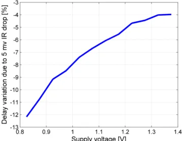
A voltage drop can lead to variations up to 10% of the nominal voltage. The consequence of a voltage variation over the circuit delay depends on the supply voltage itself, as shown in Figure 1.5 for a 5 mV voltage drop. Lower the supply voltage, larger the delay variation. This comes from the fact that the transistor switching time is determined by its drain current which, in turn, depends on the
Figure 1.5: Path delay variation in percentage to a 5 mV voltage drop depending on the supply voltage.
difference between the V and the threshold voltage Threshold voltage (Vth). In [22], the authors demonstrated that the propagation delay of a logic gate, e.g. an inverter, is proportional to the supply voltage as follows:
tswitch ∝
V
(V th − V )α (1.2)
where α is a technology-dependent factor. As it can be seen, the importance of a voltage variation ∆V increases as V gets close to Vth. Finally, voltage variations are not uniform around the die, they are spatially correlated. A voltage drop propagates through the power grid affecting each circuit logic block in a different way depending on its spatial position [23]. Handling voltage variations in recent technology nodes requires the use of local sensors or else large voltage guard-bands.
1.3
Temperature variations
Figure 1.6: Temperature variation within a chip due to hot-spots [13].
Another source of dynamic variation in CMOS circuits is the temperature. Besides fluctuations of the ambient temperature, a circuit is also susceptible to local temperature variations induced by the power dissipated by its transistors. Since an electronic circuit does not perform any chemical or mechanical work, almost all the electrical energy consumed is transformed in thermal energy. The temperature inside a circuit can vary more than 30◦C depending on the spatial position, as shown in Figure 1.6. This internal variation is due to hotspots, i.e., regions of the circuit that have a high activity and, consequently, dissipate more power. Temperature variations are slower than supply voltage ones since they have time constants ranging from miliseconds to seconds [24].
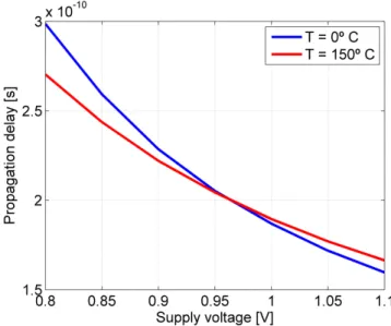
While an elevated temperature reduces the interconnect performance, the effect of temperature variations on the propagation delay of logic gates depends on the supply voltage. An increase in temperature will increase the transistor switching speed at a low value of V while the inverse is observed at a high value of V. This phenomenon is called the inverse temperature dependence (ITD). It is due to the fact that a higher temperature will reduce two transistor parameters, namely, threshold voltage and carrier mobility. Yet, these two parameters impact the transistor switching speed in opposite ways. A reduced threshold voltage leads to faster transitions while a smaller carrier mobility leads to slower transitions. As can be seen in Figure 1.7, the path propagation delay increases with the temperature for values of V above 0.95V while it decreases for values of V below 0.95V.
Figure 1.7: Demonstration of the inverse temperature dependence (ITD). A higher temperature increases the path propagation delay for values of V higher than 0.95V while the inverse is observed for V lower than 0.95V.
The circuit performance is not the only issue related to the temperature. By reducing the threshold voltage, the increase in temperature also leads to more leakage power dissipated by the transistors. Moreover, it has a direct influence on the aging-induced circuit degradation as explained in the next section. Finally, as the technology scales down, the transistor density in a circuit considerably increases. This, in turn, causes the elevation of the power density and, therefore, of the self-heating effect. Due to thermal design power constraints, parts of the circuit must be thus powered-off, the so-called dark silicon. Recent studies claimed that the amount of dark silicon may reach up to 80% of the circuit with 8nm CMOS technology [25].
1.4
Aging effects
Actually, aging effects on CMOS transistors is not a totally new topic in micro-electronics. Negative Bias Temperature Instability (NBTI) has been reported for the first time in 1966 [26]. However, it was not until recently that aging has become a real issue in CMOS circuits, when gate oxide thickness scaled to values lower than 1.5nm [27, 28]. A smaller gate oxide thickness leads to a higher oxide electric field which is the dominant factor in the main aging phenomena such as NBTI, HCI and TDDB.
1.4.1 Negative/Positive Bias Temperature Instability (N/PBTI) and
Hot Carrier Injection (HCI)
Negative Bias Temperature Instability (NBTI) consists in the degradation of PMOS transistors due to charges that get trapped inside the dielectric. These charges alter the transistor parameters over time, particularly the threshold volt-age (Vth). Vth is increased due to the trapped charges reducing the transistor switching time. NBTI is claimed to be the most prominent aging phenomenon in digital CMOS circuits [29]. Positive Bias Temperature Instability (PBTI) is the equivalent degradation in NMOS transistors. However, PBTI effect is consider-ably smaller than NBTI and it only became an important degradation mechanism after the emergence of High-κ/Metal Gate (HKMG) transistors [30].
BTI degradation is reported to be composed of two mechanisms [31], namely, a recoverable part and a permanent one. The recoverable degradation is due to charge-trapping in preexisting traps inside the dielectric. The channel charges get trapped in the dielectric when a voltage is applied on the gate and they are released to the channel when the voltage is removed. The permanent degradation is called interface state generation because it is caused by the break of Si-H bonds located at the silicon-oxide interface. Both mechanisms have an exponential dependence on the oxide electric field, determined by the supply voltage, and on the temperature [31]. An increase in temperature reduces both capture and release time of charges inside the oxide [32]. In other words, transistors get more degraded at elevated temperatures, but they also recover faster after stress is removed [33].
Hot Carrier Injection (HCI), also referred as Channel Hot Carrier (CHC) or Hot Carrier Stress (HCS), is another aging mechanism of CMOS transistors generated by charges that get trapped inside the dielectric. Likewise, its main consequence is observed as the increase in the transistor threshold voltage. The main difference is that HCI is originated from the horizontal electric field between the source and the drain, i.e. when there is a drain current flowing in the channel. HCI is caused by ”hot carriers” in the channel that gain enough kinetic energy to enter the dielectric. HCI physics are equivalent to the permanent degradation
of BTI (interface state generation) and it is thus not recoverable [34].
While BTI is impacted by the signal probability, i.e. the time the gate signal spends at a logic value (0 for NBTI and 1 for PBTI), the HCI is impacted by the signal activity, i.e. the average number of transitions. Generally, BTI is more important than HCI in digital circuits because most of the time the signals are in a static state instead of in a transition state [29]. HCI has also an exponential dependence on the supply voltage [35]. However, HCI is not strongly impacted by the temperature unlike BTI [36]. Actually, it even slightly increases at a lower temperature. HCI is therefore as important as, or even more than, BTI at low temperatures.
Besides having different origins, it is incorrect to treat BTI and HCI effects as totally independent mechanisms. This is due to the fact that some defects at the semiconductor-oxide interface are actually shared between both mechanisms. A pessimistic estimation is thus obtained by separately modelling the contribution of each effect and adding them together. However, recent works managed to accurately model the interplay of both BTI and HCI effects [37, 34].
Another issue related to BTI is its induced variability. Transistors of equal size and enduring the same stress do not necessarily produce the same Vth shift. It is due to the amount of preexisting defects inside the dielectric which has a random nature [38]. Past works have already demonstrated that time-zero variability (process-induced) and time-dependent variability (BTI-induced) are not correlated [39]. The local Vth variability therefore increases over time due to BTI. On the other hand, it is reported that HCI has a stronger dependence on time-zero parameters and, therefore, it does not induce more variability [40].
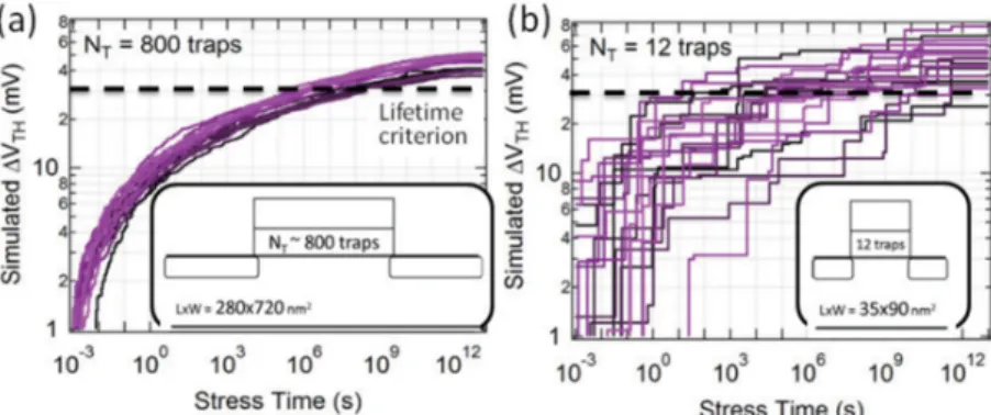
Moreover, the average number of preexisting defects inside the oxide decreases as the technology scales down. This leads to an exponential growth of the time-dependent variability in addition to the time-zero variability increase previously discussed in Section 1.1.2. Figure 1.8 shows the simulated Vth shift for transis-tors with dimensions equal to 280 × 720nm2 and for transistors with 35 × 90nm2 dimensions [41]. As it can be seen, the increase in variability caused by the re-duced number of defects is impressive. Nevertheless, the BTI-inre-duced variability is an important issue for analog circuits and SRAM memories while for digital circuits the mean degradation is more relevant [42].
1.4.2 Destructive aging effects
BTI and HCI are the most important aging effects, but they are not the only ones. While they induce a gradual shift in the transistor parameters, the other effects lead to destructive events which may result in a total failure of the circuit. Time-Dependent Dielectric Breakdown (TDDB) is another phenomenon that occurs inside the dielectric. TDDB is characterized by the creation of a conductive path inside the dielectric caused by trapped charges. Like BTI, the charges are
Figure 1.8: Simulated Vth shift due to BTI for transistors with (a) 800 defects and (b) 12 defects. The reduced number of preexisting defects, which is related to transitor size, leads to a considerable increase in local variability [41].
trapped inside the dielectric when a high electric field is applied on the dielectric. This conductive path increases the leakage current and may turn the transistor inoperative. Some soft breakdowns gradually increase the leakage current before the occurrence of the hard breakdown, when a path is created through the gate to substrate.
Electromigration (EM), Stress Migration (SM) and Thermal Cycling (TC) are aging mechanisms that affect the interconnects. Electromigration is due to the momentum transfer between conducting electrons and diffusing metal atoms caused by the current that flows in the wires. EM provokes small voids in the interconnects which may result in an open circuit.
Stress Migration is induced by mechanical stress and can also lead to an open circuit in the interconnects.
Finally, Thermal Cycling is due to elevated temperature gradients. Permanent damage accumulates during large variations of temperature and may eventually lead to failures in the interconnects and packaging.
Models for all the aging effects listed here can be found in [43]. In this thesis we focus only on BTI and HCI effects since we are interested in modeling the circuit performance degradation. The other aging effects are thus not addressed hereafter.
1.5
Conclusion
This chapter introduced all sources of variability in digital CMOS circuits, namely, PVT variations and aging effects. Process variations are caused by manufactur-ing and atomistic limitations. They can lead to permanent changes in the circuit performance and leakage power from expected values. Voltage variations are mainly due to the circuit impedance. They provoke very fast fluctuations of the
circuit performance, in the order of nano- and microseconds. Local temperature variations are induced by different activities and, as consequence, power dissi-pation between the circuit blocks. Finally, aging effects, in particular BTI and HCI, manifest through carriers that get trapped inside the dielectric. These aging mechanisms cause gradual degradation of the transistor characteristics reducing the circuit performance over time.
The continuous technology scaling is making hard to design resilient and energy efficient circuits. Reduced transistor size increases both random process variations and aging effects due to the atomistic nature. Each missing/extra dopant or carrier has a greater relative importance as the number of atoms inside a transistor is reduced. Besides, circuits are more susceptible to voltage variations as the voltage scales down while the circuit impedance does not scale at the same rate. Finally, increased transistor density leads to more power density and, consequently, more temperature deviation within a circuit.
The use of safety guard-bands is not anymore suitable due to the considerable waste of energy imposed by it. As shown in Figure 1.9, voltage margins necessary to address the worst case scenario for every source of variability constitute an im-portant part of the supply voltage. The following chapter discusses thus existing solutions to handle variability in digital circuits. These solutions increases the energy efficiency by reducing the safety guard-bands while avoiding timing faults.
Figure 1.9: Recent technology nodes require large voltage guard-bands to cope with all sources of variability, namely, process, temperature, voltage and aging variations.
Techniques for coping with
variability in digital circuits
In Chapter 1, we introduced the sources of variability and their impact on digital circuits. In the present chapter, we first discuss the traditional approach adopted by designers to handle variability. This approach basically consists in modelling the variations and using simulator tools during the design phase to calculate the timing margins needed to avoid timing faults. However, this approach has become no longer suitable as the technology scaled down and the variability exacerbated because it leads to large guard-bands that do not allow to use the circuit at the best of its capabilities in terms of energy efficiency.
Adaptive techniques have emerged as an important research topic in the last years to reduce the margins fixed by the circuit designers. These techniques implement a strategy to on-line adapt the circuit against variations. The adap-tation can be done through a variable supply voltage source or/and a variable clock generator. Some examples are briefly discussed here. We also discuss the adaptive body bias, a technique that has arisen with FD-SOI technologies. Next, we present some sensors for on-line tracking the variability. This comprises mon-itors for tracking the fluctuation of the critical path timing as well as for directly measuring PVT and aging variations.
Lastly, this chapter analyzes the impact of aging effects on an environmental variability monitor. The use of such monitor is essential in adaptive architectures to track local variations of the supply voltage and the temperature. Still, it is susceptible to aging as any other circuit element. Thus, it becomes less reliable over time. Therefore, we propose a recalibration methodology to mitigate the impact of BTI and HCI on the estimates provided by the monitor making it robust against aging.
2.1
Introduction
Even though asynchronous logic arises as a promising solution to reduce power dissipation and increase robustness to variability [44], nearly all digital circuits are still based on synchronous logic. A synchronous circuit is composed of memory elements, mainly flip-flops, synchronized by a common clock signal. All flip-flops in the circuit simultaneously update their outputs, based on their respective input signals, on the rising edge of the clock (sometimes on the falling edge or even on both edges).
Figure 2.1: Example of a setup time violation occurring in the second clock rising edge. The input data ((D)) arrives at the flip-flop at the same time as the clock rising edge resulting in a timing fault, i.e. the logic value stored in the flip-flop ((Q)) remains ’1’ instead of changing to ’0’.
One of the main concerns for digital circuit designers is thus to avoid setup time violations, also called timing faults. A setup time violation occurs when a data arrives at the flip-flop too close or after the clock rising edge. This makes the flip-flop to store a possibly wrong value. Finally, a timing fault may lead to an error in the circuit operation. This can be catastrophic in safety-critical systems like automotive and aviation ones. Figure 2.1 shows an example of a timing fault. The value latched by the flip-flop in the second clock rising edge is not the correct one. The input data transitions too late, making a logical ’1’ to be stored in place of a logical ’0’.
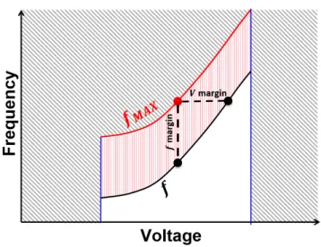
The data arrival time is determined by the propagation delay of the path that diffuses it. The path propagation delay, in turn, depends on all sources of vari-ability introduced in the previous chapter, namely, process, voltage, temperature and aging. As stated in Session 1.2, the propagation delay is inversely linear to the supply voltage V (for values of V sufficiently higher than the threshold voltage Vth). Therefore, designers usually add voltage margins to V in order to reduce the propagation delay and thus avoid timing faults despite the presence of variations. As shown in Figure 2.2, either a higher voltage (V margin) or a lower frequency (f margin) is adopted.
Figure 2.2: Safety margins are used to handle PVT and aging variations. fM AX
is the nominal frequency for a given supply voltage, while f is the actual clock frequency taking into account safety margins. These margins can be either a lower frequency (f margin) or a higher voltage (V margin).
Nevertheless, the power dissipated by the circuit strongly depends on V . The power is composed of two components, namely, dynamic and static. Dynamic power is due to the charging and discharging of capacitances originated by the change of state of the transistors. It represents then the power dissipated when the circuit is active. The dynamic power Pdyn dominates the power consumption
in CMOS circuits and it is related to the supply voltage V as follows:
Pdyn∝ αf V2 (2.1)
where α is the activity factor, i.e. the percentage of transistors switching, and f is the clock frequency. The static power, on the other hand, is due to the leakage current. It represents the amount of power dissipated when the circuit is in an idle state. Leakage currents depend on Vth and, consequently, on the temperature T . Besides smaller than the dynamic power, the importance of static power has considerably increased with technology scaling due to the reduced Vth. The static power Pstat dependence on both V and T can be expressed as:
Pstat∝ βVγeδT (2.2)
where β, γ and δ are technology- and circuit-dependent parameters. As can be seen from equations (2.1) and (2.2), the use of excessive voltage guard-bands leads to a significant energy loss. Designers must thus accurately estimate the minimum voltage margin needed for a correct operation of the circuit in order to obtain the most energy efficient circuit.
A statistical characterization of the transistor parameters is performed by the semiconductor foundries for each new technology node [45]. This characterization generates device-level models that are used by Electronic Design Automation (EDA) tools to assess the circuit timing characteristics. Besides the mean value, the characterization also provides the standard deviation σ for each transistor parameter. This allows the assessment of the circuit timing for many process variations. For voltage and temperature variations, σ depends on the mission profile, i.e. the circuit application. However, the number of possible corners can reach up to 220combinations making it impossible to assess the circuit timing for each corner [46]. Therefore, the traditional approach consists in identifying the circuit critical paths and in calculating their propagation delay for the worst-case corner of PVT variations through Static Timing Analysis (STA) [47]. The best-and worst-case values are usually defined as ±3σ from the mean value.
The main drawback of this approach is that it leads to an over-pessimistic estimation of the circuit performance, the probability of worst-case scenario hap-pening being very low. Actually, in some cases it is even zero due to the correla-tion between process variacorrela-tions that makes not all conjunccorrela-tion of values feasible. Furthermore, the worst-case process corner is not necessarily equivalent to the worst-case performance corner [48]. Basically, there exist an interaction between transistor parameters so that some specific combinations of values can lead to a performance worse than the combination of worst-case values.
Another way to estimate the safety guard-bands is through Monte-Carlo anal-ysis [49]. It consists in running hundreds or thousands of simulations with random values for the transistor parameters extracted from their respective probabilistic distribution. This is a ”brute force” method to statistically evaluate the propa-gation delay of the critical paths. Its main shortcoming is the excessive compu-tation time required to obtain a representative amount of simulation data. An alternative to Monte-Carlo analysis is Statistical Static Timing Analysis (SSTA) [50]. This approach is similar to STA but it uses probability distributions for the timing of gates and interconnects instead of deterministic values.
To summarize, constant advances in the EDA industry have made the circuit timing estimation a quite matured process. Nowadays, designers have several means for accurately assessing the critical path propagation delay in the worst-case scenario. Nevertheless, the aggressive scaling of the transistor dimensions has exacerbated the impact of variability on digital CMOS circuits, as stated in Chapter 1. Significant voltage margins lead to huge energy losses that cannot be afforded, in particular for mobile applications with limited battery life.
2.2
Adaptive architectures
Adaptive architectures have emerged in the last years to cope with local variabil-ity in digital circuits without the need of large guard-bands. Adaptive circuits implement a sense-and-react scheme usually based on Dynamic Voltage and Fre-quency Scaling (DVFS). Basically, a DVFS system integrates two actuators, namely, a variable voltage supplier and a variable clock generator. These actu-ators dynamically change the circuit supply voltage V and the clock frequency f depending on the required performances. This approach reduces the energy consumption by lowering the power dissipation when there is no need for a high performance. However, in a DVFS system, the V /f couples are predefined in the design phase, with safety margins incorporated to avoid timing faults. The Adaptive Voltage and Frequency Scaling (AVFS) technique consists in employ-ing embedded sensors to track the variability in addition to the actuators used for DVFS. By implementing a closed-loop control, V and/or f can be dynami-cally changed to adapt against variability. Therefore, AVFS increases further the energy efficiency of the circuit by reducing the safety guard-bands.
Figure 2.3: General architecture of an AVFS system.
A general architecture of an AVFS system is shown in Figure 2.3. The small black squares inside the Core block correspond to the embedded monitors. They provide information regarding the local variability for the Local adjustment block. This latter is in charge of checking if the circuit is operating at a safe and energy efficient point. It then notifies the Local control block of the need of changing the operating conditions to either avoid timing faults or increase the energy efficiency. Finally, the Local control manages both the voltage and the frequency actuators based on this information and on the performance constraints provided by a higher-level control. The objective is to always maintain the clock frequency f as close as possible to the maximum functional frequency fM AX, as shown in
2.2.1 Adaptation strategies
In AVFS systems, the change of operating conditions can be done through two variables, the clock frequency and the supply voltage. Generally, while one ac-tuator is used for adaptation purpose, the other remains constant or is set so as to satisfy the performance constraints, like in a DVFS system. A circuit that adapts itself through the clock frequency is called AFS system. As shown in Figure 2.4(a), the values of V are fixed according to the performance levels while f is dynamically changed to deal with variability. Similarly, Adaptive Voltage Scaling (AVS) is when the adaptation is done through the supply voltage, see Figure 2.4(b).
(a) AFS principle, V values are prede-fined while f is used for adaptation.
(b) AVS principle, f values are prede-fined while V is used for adaptation.
Figure 2.4: AFS and AVS strategies with 3 performance levels.
Supply voltage actuator
The first works that focused on adaptive techniques for dealing with static and dynamic variability date back to the 90s [51, 52, 53, 54, 55]. They are all based on AVS which is usually preferred over AFS since the circuit performance is not modified. In these works, the supply voltage V is dynamically changed to its minimum functional value Vminbased on the information regarding the variability
provided by a monitoring system.
In general, a DC/DC buck converter is used as voltage actuator. Figure 2.5(a) illustrates the standard architecture of a DC/DC buck converter. This circuit converts a DC voltage V dd supplied by the main power supply to a lower DC voltage V out. It is composed of a Pulse Width Modulator (PWM) block that controls the PMOS and NMOS transistors based on an internal ramp. The PWM block is governed by an internal control that generates a command depending on the required voltage V ref and on the current output V out. Finally, an LC filter
(a) Standard architecture of a DC/DC buck converter.
(b) Principle of the Vdd-hopping.
Figure 2.5: Different types of voltage actuators.
reduces the output ripple. This kind of voltage actuator presents great stability and robustness to variability due to its closed-loop control. However, its large area, in particular due to the LC filter, limits its implementation in small circuits. Furthermore, it presents a poor efficiency at low voltages, which is the case of low-power circuits.
To overcome these limitations, recent works [56, 57, 58] adopted an adap-tation strategy based on Vdd-hopping technique, also called voltage dithering. Figure 2.5(b) depicts its principle. Vdd-hopping consists in switching the volt-age between two or more predefined V dd levels to achieve an output voltvolt-age Vout equals in mean value to Vref. This kind of actuator has a very small area
and a fast voltage transition time. However, unlike the DC/DC buck converter, the Vdd-hopping technique has a discrete number of voltage levels. For this reason, Vdd-hopping seems more suitable for changing the performance level (Figure 2.4(a)) than for adapting against variations (Figure 2.4(b)).
Clock frequency actuator
In some cases, AFS may be a better choice than AVS since its implementation is less complex, no impact on the power distribution system, and the time dynamics of frequency actuators are considerably smaller, allowing a faster adaptation to dynamic variations. In an AFS system, the clock frequency f is dynamically controlled to stay always at its maximum functional value fM AX. This is done
through a variable clock generator, usually a Phase-Locked Loop (PLL) [59, 60, 61]. PLLs use a Voltage-controlled oscillator (VCO) to generate the oscillating signal. A phase detector compares the output signal frequency with the reference frequency while a filter ensures the actuator stability. Figure 2.6(a) [62] shows an example of a all-digital PLL. This kind of actuator is robust to variability and provides a low-jitter clock signal. However, it has a high area cost which impedes its replication in a multi-core circuit to apply local AVFS in each core.
Another frequency actuator, known as Frequency-Locked Loop (FLL), has thus been developed to overcome this limitation of PLLs. A FLL has a similar
architecture than PLL, also generating a clock signal from a VCO. The difference lies on the way they compare the output frequency with the reference one. In an FLL, the comparison is done directly through the frequency instead the phase. That is why its circuit is much more simpler, as shown in 2.6(b) [63]. The authors in [63] claim that the area of the proposed FLL is 4 to 20 times smaller than a classical PLL. Moreover, its response time is way faster, allowing a transition of frequency level in a few clock cycles. In [58], a digital FLL is used to locally generate a clock signal inside each core of a multi-core circuit with output fre-quency ranging from 2.9 GHz down to 15 kHz. The area cost was not reported, but the same FLL was adopted in another multi-core architecture [64] with an area overhead of only 0.3% of each cluster.
(a) Example of digital PLL [62]. (b) Example of digital FLL [63].
Figure 2.6: Different types of frequency actuators.
Body bias voltage
Besides AVS and AFS, a new adaptation strategy has recently emerged, Adaptive Body Bias (ABB). MOSFET transistors have a fourth terminal called body which is generally connected to the source. However, it is possible to modulate the transistor threshold voltage Vth by applying a source-to-body voltage, also called Body bias voltage (Vbb). Vth is increased when a positive Vbb is applied, known as reverse body-bias (RBB). This leads to a reduced leakage current with a slower switching speed as side effect. Conversely, forward body bias (FBB), i.e. applying a negative Vbb, reduces Vth and, as a consequence, leads to faster transistors although with increased leakage current.
The use of ABB was first proposed in early 2000s [65, 66, 67]. Initially, it was adopted to compensate die-to-die process-induced Vth variations. For instance, [67] claimed to reduce the frequency variation σ/µ1 between dies from 4.1% to 0.69% by applying ABB. Better results were achieved by applying different values of Vbb to each circuit block in order to tackle within-die variations. This approach reduced further the frequency variation σ/µ to only 0.21%. The reported area
1
overhead due to the ABB generator and its control block is from 2% to 3% of the total die area.
The development of Ultra-Thin Body and Box Fully-Depleted Silicon-On-Insulator (UTBB FD-SOI) CMOS technologies in the last years has boosted the benefits of ABB. UTBB FD-SOI enables the use of a wide range of body bias voltage. Vbb can vary up to ±3.0V in UTBB FD-SOI technologies while in bulk-based technologies it was limited to ±0.5V [68]. It is widely reported that FBB increases both the performance and the energy efficiency of digital circuits in UTBB FD-SOI, either at low or high values of Vdd [61, 69]. Many recent works have thus focused on the choice of using dynamic Vdd or dynamic Vbb to find the best performance/energy trade-off. Usually, the best choice is their joint use since each strategy presents better results depending on the operating conditions (clock frequency, temperature, circuit activity, ...) [70, 71].
With regard to reliability, [72] showed that FDSOI and bulk transistors have similar sensitivities to both BTI and HCI effects. Later, [73] demonstrated the benefits of using ABB over AVS in FDSOI technology. Firstly, transistors endure more degradation when a higher Vdd is applied to compensate aging variations instead of using FBB. Secondly, AVS also increases the power dissipation while the power remains constant with ABB. Besides the benefits in energy and re-liability, the implementation of ABB is also simpler. Unlike AVS, it does not require substantial consideration of IR drop and it has a low static current since its load is almost purely capacitive [74]. However, Vbb management is not yet a fully mature technique as supply voltage and clock frequency management, this is why AVS and AFS are more popular strategies.
2.3
Monitoring systems
The choice of adaptation strategy and actuators is important to optimize the energy efficiency of the circuit. However, the monitoring system plays a critical role because it is in charge of ensuring that the circuit is operating in a ”safe zone”, i.e. without timing faults. Moreover, it must ensure that the clock frequency is as close as possible to its maximum functional value. An inaccurate monitoring system can thus result in either an unreliable or an energy inefficient circuit.
Likewise the adaptation strategy, the monitoring of the different roots of variability in an AVFS system can be done in different ways. They can be split in two major categories. The first one consists in timing fault detection and fM AX tracking techniques. Sensors int this category focus on monitoring the
variation of the critical path slack time to detect either the pre-occurrence or the occurrence of a timing a fault. Thus, they use a critical path replica or they are placed on the critical paths. The other category is the direct measurement of the variability. This category of monitors provides a numerical measurement of one
of the source of variations, i.e. process, voltage, temperature or aging.
2.3.1 Timing fault detection and fM AX tracking
The first work to implement a fM AX tracking technique to reduce safety margins
was [51]. The authors implemented an AVS system using a PLL to track the variability, as shown in Figure 2.7(a). The supply voltage is regulated until the VCO frequency matches the clock frequency fin. This technique is based on the fact that the circuit critical paths and the VCO ring-oscillator have the same sensitivity to PVT variations. This assumption might be true for the technology used in [51] (2µm), but this is no more valid for the current technologies.
The same concept of variability monitoring has been better developed in [55] for a complete AVFS system. A DC/DC buck converter adjusts its output voltage based on the frequency of a ring oscillator supplied by the DC/DC converter. This ring-oscillator is also used as frequency actuator generating the clock frequency for the CPU, as shown in Figure 2.7(b). Implemented in 0.6µm technology, the authors claim that a energy reduction of 78% is achieved compared to a system without AVFS. Still, circuits have different sensitivities to static and dynamic variations depending on their topology. Each critical path has a specific topology which is much more complex than the topology of a ring-oscillator. Moreover, such monitor does not endure the same local variability than the logic circuit. Therefore, it is not enough to determine the circuit performance fluctuation in advanced technology nodes.
(a) PLL implemented in [51] to adapt the supply voltage against variations.
(b) In [55], the ring-oscillator is used at the same time to generate the clock fre-quency and to monitor the variability.
![Figure 1.2: The number of dopant atoms per transistor is reduced with technology node [16].](https://thumb-eu.123doks.com/thumbv2/123doknet/12859337.368460/23.892.264.602.340.596/figure-number-dopant-atoms-transistor-reduced-technology-node.webp)
![Figure 1.3: Local threshold voltage variation σ V th induced by random dopant fluctuation (RDF), line edge roughness (LER) and oxide thickness fluctuation (OTF) versus technology node [20].](https://thumb-eu.123doks.com/thumbv2/123doknet/12859337.368460/24.892.288.624.387.646/figure-threshold-variation-fluctuation-roughness-thickness-fluctuation-technology.webp)
![Figure 2.7: Pioneer works that used a ring-oscillator to track f M AX [51, 55].](https://thumb-eu.123doks.com/thumbv2/123doknet/12859337.368460/41.892.166.700.704.939/figure-pioneer-works-used-ring-oscillator-track-ax.webp)
![Figure 2.10: Throughput increase and energy reduction achieved with Bubble Razor [79] compared to a margined design and to a CPR approach (canary).](https://thumb-eu.123doks.com/thumbv2/123doknet/12859337.368460/44.892.183.739.656.860/figure-throughput-increase-reduction-achieved-compared-margined-approach.webp)
![Figure 2.15: Distribution of the normalized degradation of the logic circuit (black circles) and of the CPR (red squares) [112].](https://thumb-eu.123doks.com/thumbv2/123doknet/12859337.368460/51.892.209.658.148.430/figure-distribution-normalized-degradation-logic-circuit-circles-squares.webp)
![Figure 2.16: Multiprobe sensor for dynamic variability monitoring [114].](https://thumb-eu.123doks.com/thumbv2/123doknet/12859337.368460/52.892.270.642.148.414/figure-multiprobe-sensor-dynamic-variability-monitoring.webp)
