HAL Id: hal-00441820
https://hal.archives-ouvertes.fr/hal-00441820
Submitted on 17 Dec 2009
HAL is a multi-disciplinary open access
archive for the deposit and dissemination of
sci-entific research documents, whether they are
pub-lished or not. The documents may come from
teaching and research institutions in France or
abroad, or from public or private research centers.
L’archive ouverte pluridisciplinaire HAL, est
destinée au dépôt et à la diffusion de documents
scientifiques de niveau recherche, publiés ou non,
émanant des établissements d’enseignement et de
recherche français ou étrangers, des laboratoires
publics ou privés.
Impact of substrate coupling induced by 3D-IC
architecture on advanced CMOS technology
Maxime Rousseau, Marie-Anne Jaud, Patrick Leduc, Alexis Farcy, Antoine
Marty
To cite this version:
Maxime Rousseau, Marie-Anne Jaud, Patrick Leduc, Alexis Farcy, Antoine Marty. Impact of substrate
coupling induced by 3D-IC architecture on advanced CMOS technology. European Microelectronics
and Packaging Conference, Jun 2009, Rimini, Italy. �hal-00441820�
Impact of substrate coupling induced by 3D-IC architecture
on advanced CMOS technology
Maxime Rousseau
1,3,4, Student Member, IEEE, Marie-Anne Jaud
2, Patrick Leduc
2,
Alexis Farcy
1and Antoine Marty
3,41
STMicroelectronics - 850 rue Jean Monnet - 38926 Crolles cedex, France
2
CEA-LETI/MINATEC - 17 rue des Martyrs - 38054 Grenoble cedex 9, France
3
CNRS ; LAAS ; 7 avenue du colonel Roche, F-31077 Toulouse, France
4
Université de Toulouse ; UPS, INSA, INP, ISAE ; LAAS ; F-31077 Toulouse, France
Phone: +33 4 38 78 06 35, fax: +33 4 38 78 50 12, mail: maxime.rousseau@cea.fr
Abstract
A TCAD-based simulation approach is proposed to study the impact of transient coupling that occurs within a generic 3D integration on 65 nm technology based CMOS devices. This coupling is mainly due to signals applied on redistribution layer (RDL) and through-silicon vias (TSV). These both 3D-inherent metal structures may cause variations on normal operating conditions of advanced devices. Influence of design and technology parameters such as keep-away zone, TSV/RDL isolation oxide thicknesses and remaining silicon thickness are investigated on NMOS transistors, in order to extract application-driven 3D-specific design rules. We also show that significant variations on saturation drain current and especially on leakage current appear each time TSV/RDL-applied signals switch. These current variations are strongly dependent on rise and fall potential ramp times applied on TSV or RDL. Shorter rise or fall ramp time induces a more aggressive coupling on devices. In certain cases, it may be destructive for advanced CMOS technology. Dynamic variations on saturation drain current can be tolerated under specific design rules and process options but those on leakage current are very important compared to static leakage current value, and are of the order of 10-6 A/µm.
Key words: 3D integration, through-silicon via, redistribution layer, substrate coupling, TCAD, device performance.
Introduction
As 2-dimensional IC scaling becomes more and more difficult to achieve for the next technological nodes, 3D integration technology is being considered as a real breakthrough approach. It seems to be an interesting solution in terms of IC design and manufacturing [1,2]. 3D integration doubtlessly brings significant benefits concerning circuit performance, density of integration, interconnect power consumption and heterogeneous technology integration capabilities [3].
Microelectronics worldwide actors tend to develop a through-silicon via technology (TSV) in order to interconnect stacked ICs. TSV appears to be one of the greatest technology challenges brought by 3D integration. But the redistribution layer (RDL) can also be considered as a brand new entity in conventional IC architectures. RDL features large metal lines implemented on the backside of the thinned active stratum. Many papers showed that 3D integration process has no impact on CMOS technology, or very limited [4-5]. Beyond process issues, the fact is that both structures are needed for power, I/Os and signal routing through all the thinned strata, leading to electrical parasitic coupling
and critical substrate noise on neighboring active devices [6]. This coupling might be restrictive for design capabilities and needs to be quantified as a function of layout and technology parameters, such as keep-away zone, TSV/RDL isolation oxide thicknesses and remaining silicon thickness. This will lead to define tunable 3D-specific design rules that will ensure reliable circuit design according to the application choice. In a first time, we propose to explain our 2-dimensional TCAD-based simulation methodology. Then, the impact of technology and layout parameters – in case of TSV or RDL induced coupling – is investigated on NMOS transistors. From that point, a specific structure for 3D integration is set and the impact of various TSV-applied potential ramp times is investigated. Simulation methodology
Two dimensional TCAD (Technology Computer Aided Design) transient simulations [7] have been performed on a 3D integration structure (described on figure 1). Drift-diffusion transport model with usual mobility model of Lombardi and Shockley-Read-Hall generation rate are used.
Figure 1. 2-D structure of the thinned active stratum.
3D integration can be implemented with various device technologies. This paper focuses on 65 nm bulk CMOS devices integrated with high-density TSV. Silicon substrate is thinned in the range of 5 to 30 µm (TSUB). Thinned active stratum
is bonded face to face with the bottom active stratum. As only electrical coupling phenomena occurring within the thinned stratum are considered, all other integration process steps do not impact our methodology. This study can be applied to a majority of case.
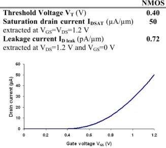
Simulated NMOS transistor features low power 65 nm bulk technology [8]. The channel length is 1 µm in order to avoid short-channel effects. The doping profile of the P-doped well is based on SIMS measurement. Intrinsic doping level for bulk silicon is 10+15 cm-3. Table 1 refers to the electrical characteristics of the simulated transistor. The electrical output characteristics IDS(VGS)
calculated at VDS=1.2V is plotted on Figure 2. The
saturation drain and leakage currents demonstrate rather accurate performance for this range of channel length.
TSV and RDL are respectively considered as intra bulk and backside electrodes – independent from each other and isolated from the thinned substrate with an appropriate oxide layer. TSV and RDL isolation oxide thicknesses are two important technology parameters. They are respectively noted as TOXTSV and TOXRDL.
In this work, we propose to observe how a square signal applied independently on these two electrodes may impact the electrical characteristics of the NMOS transistor. In order to understand how the substrate coupling occurs within the structure, the three technology parameters previously described as TSUB, TOXTSV and TOXRDL, and a layout
parameter, namely “keep-away zone”, are investigated in the simulation methodology. The range of dimensions for each parameters investigated hereafter are listed in Table 2.
The MOS transistor is plugged on its static mode (VGS = VDS = 1.2 V). A square voltage (f =
200 MHz, 50 ps-long rise and fall ramp time, 1.2 V peak voltage) is then applied on the TSV or on the RDL. The saturation drain current IDSAT and the
local body potential Vbody, located in between the
conduction channel at 5 nm under the gate
oxide-silicon interface, are extracted during the transient analysis. This position enables to quantify the finest electrical disturbances that may modify the electrical behavior of the transistor.
Table 1. Electrical characteristics of the simulated Low Power NMOS transistor with a channel length of 1 µm.
NMOS Threshold Voltage VT (V) 0.40
Saturation drain current IDSAT (µA/µm)
extracted at VGS=VDS=1.2 V
50 Leakage current ID leak (pA/µm)
extracted at VDS=1.2 V and VGS=0 V
0.72
Figure 2. IDS(VGS) characteristics at VDS=1.2V of
the simulated NMOS transistor.
Table 2. Range of dimension of the parameters investigated in this work.
Dimension range (µm) Substrate thickness (TSUB) 5 - 30
TSV isolation oxide thickness (TOXTSV) 0.05 - 0.5 RDL isolation oxide thickness (TOXRDL) 0.4 - 1.4 Keep-away zone 2.5 - 5
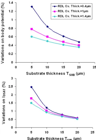
TSV-induced substrate coupling
Following the methodology described above, variations on body potential Vbody and saturation
drain current IDSAT are extracted during transient
analysis. Maximum dynamic variations for both are reported on Figure 3 as a function of remaining substrate thickness TSUB after grinding for different
TSV isolation oxide thicknesses TOXTSV. Potential
and current variations follow the same behaviour. It is shown that a thicker oxide for TSV isolation reduces significantly variations on channel potential (3 % to 1,5 %) and saturation current (5,5 % to 2,5 %) because of the decrease of TSV oxide capacitance. In all cases, increasing the oxide thickness for TSV isolation from 50 nm to 500 nm makes decreasing the coupling in a range of 50 %. Silicon substrate thickness has a rather low impact on dynamic variations of current for thickness in the range of 10 to 30 µm. For thickness lower than 10 µm, the bulk resistance between TSV and active
area increases and the TSV oxide capacitance decreases. The consequence is a significant decrease of TSV-induced coupling. TOXTSV=0.05µm TOXTSV=0.5µm TOXTSV=0.05µm TOXTSV=0.5µm TOXTSV=0.05µm TOXTSV=0.5µm TOXTSV=0.05µm TOXTSV=0.5µm
Figure 3. Maximum dynamic variations on body potential (top) and IDSAT (bottom) for NMOS
transistor as a function of substrate thickness TSUB for two TOXTSV values: {0.05 µm; 0.5 µm}
and two keep-away zones: 2.5 µm (full lines) and 5 µm (dotted lines).
As well as technology parameters, layout design may impact the coupling on CMOS devices. For instance, the position of bulk contact, that helps to control the body potential, and the position of the closest active area beside the TSV edge (the so-called keep-away zone), may control more or less substrate coupling. As the bulk contact is always implemented close to a single transistor, the dimension of the STI located between the bulk contact and the source area (cf. Figure1) is set at 200 nm for all simulations. Only the impact of keep-away zone is investigated and reported on Figure 3.
The first keep-away zone at 2.5 µm is the minimum distance allowed because of the 2 µm guard for TSV alignment. The second keep-away zone at 5 µm is the typical distance not to be exceeded to keep density of device integration as high as possible. If referring to Figure 3, it seems obvious that keep-away zone, taken in this range of
dimensions, does not have enough impact to decrease coupling, compared to the influence of technology parameters. The bulk contact seems to be unsufficient to control accurately the body potential, almost independently of its position. The fact is TSV-induced coupling occurs all along the TSV, so that substrate noise propagates at the same time through the low-resistivity doped well, and through the high-resistivity bulk silicon. The lower resistivity of the active area (because of its high doping level compared to bulk silicon) makes easier the noise propagation. As the TSV has a thin isolation thickness, it can be assumed that TSV behaves like a parasitic oxide capacitance that bulk contact cannot control because of the large dimensions of the structure (bulk contact has a very localized effect). For the following, we set the keep-away zone at 2.5 µm.
By referring to Figure 3, thinning down the substrate to 5 µm - or below if possible - decreases the substrate coupling. But this will place the RDL line closer to active devices, so that RDL-induced coupling may increase.
RDL-induced substrate coupling
Impact of RDL-induced substrate coupling is reported on Figure 4.
Figure 4. Maximum dynamic variations on body potential (top) and IDSAT (bottom) for NMOS as a
function of substrate thickness TSUB for various
As expected, maximum variations on body potential and saturation drain current are observed for the thinnest substrates. Compared to previous TSV study, RDL-induced noise coupling seems to be less substantial. Maximum variation on IDSAT is
lower than 2.5 % for minimum RDL isolation oxide thickness (400 nm). As for TSV isolation, a thicker RDL isolation makes decreasing the coupling. Moreover, from 15 µm-thick substrate and above, there is no more effect of RDL isolation thickness on variations of saturation drain current. It may be due to the fact that RDL isolation behaves like an oxide capacitance whose effect decreases when the bulk resistance increases with thicker silicon substrate. Coupled impact of TSV and RDL
It was explained how TSV and RDL structures produce substrate noise independently and what typical response on active devices is. Considering the TSV is connected to the RDL line – meaning that the same signal is applied on both structures - their respective coupling noise can be added to obtain the global substrate noise produced by 3D architecture. The global response on NMOS saturation drain current is depicted on Figure 5, for equivalent thickness of TSV and RDL isolation (400 nm). The highest coupling response on IDSAT is
obtained for the thinnest substrate (5 µm). At a glance, the global behaviour of the curve is driven by RDL coupling behaviour, mainly because the TSV coupling remains rather constant around 2 and 3 %. Beyond that, the global coupling jointly produced by TSV and RDL may be considered as mainly driven by TSV from 15 µm thick and more because of the significant decrease of RDL coupling for this range of substrate thickness.
Figure 5. Contributions of TSV and RDL induced coupling on saturation drain current.
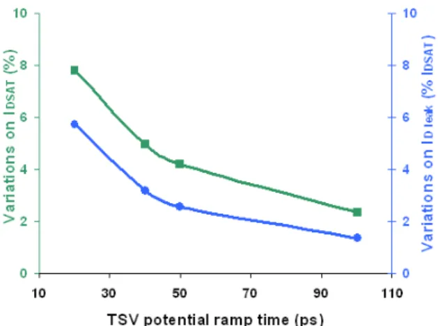
Impact of TSV potential ramp times on coupling It was demonstrated that substrate noise is produced by 3D integration, i.e. TSV and RDL structures, when a square signal is applied.
Figure 6. Maximum dynamic variations on IDSAT
(green squares) and ID leak (blue circles expressed
in terms of % IDSAT) for NMOS as a function of
various rise and fall ramp times applied on TSV (from 20 ps to 100 ps).
As variations on IDSAT and channel potential
are only detected during TSV/RDL potential ramp time, parasitic potential may have a scalable impact depending on its ramp time. In this part, similar results as previously described are reported for increasing TSV potential ramp times, from 20 ps (most aggressive ramp time in CMOS65 technology) to 100 ps. Moreover, leakage current (IDS for
VDS = 1.2 V and VGS = 0 V) is also investigated.
These results are summarized in Figure 6. For this study, substrate thickness is 5 µm, keep-away zone is 2.5 µm and oxide thickness for TSV isolation is 50 nm (worst case).
NMOS currents seem to be affected quite similarly. Variations on saturation drain current and variations on leakage current are expressed in the same unit (% IDSAT) so that they can be compared to
each other. Variations on leakage current appear dramatically important because in the range of those on IDSAT (see Table 1 for static current values).
In all cases, and independently of the ramp time, the dynamic variation on leakage current is really critical for logic circuits. It means that the transistors could be turned on temporarily while the off state is established.
The strongest impact on drain currents is shown to appear with the shortest ramp time applied on TSV potential, here 20 ps. In that case, maximum IDSAT variation is 8 %. For instance, 10 % is the
maximum accepted value for static IDSAT shift after
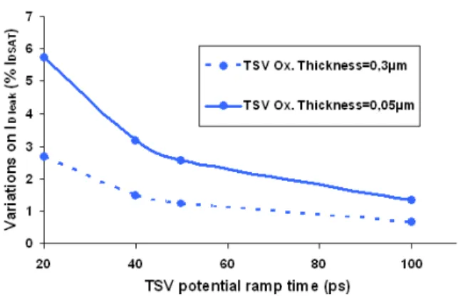
5-year-long normal operation (transistor aging). The effect of TSV isolation oxide thickness TOXTSV is also investigated regarding the results on
drain leakage current for various TSV potential ramp times. These results are reported on Figure 7. It is shown that an increase of TSV isolation oxide thickness from 50nm to 300nm decreases the impact on leakage current of only 50 %. That makes typical shifts on leakage current in the range of 10-7 to 10-6 A/µm compared to its static value at 10-13 A/µm.
Figure 7. Maximum dynamic variations of leakage current for NMOS transistor at various TSV potential ramp times for two values of TOXTSV: 50 nm (solid lines) and 300 nm (dotted
lines).
In all cases, the variations on both currents only occur during the parasitic signal ramp time. Once the TSV potential remains static in either its state ‘on’ (1.2 V) or ‘off’ (0 V), no more electrical coupling occurs through the substrate. Leakage current or saturation drain current go back to their initial static values.
Conclusion
Through-silicon vias and redistribution layers, respectively considered as intra bulk and backside electrodes, generate dynamic parasitic coupling within the thinned silicon substrate in a high density 3D integration. This dynamic noise propagates through the thin silicon, mainly in the active area where the resistivity is lower than in the bulk silicon. It was also shown that bulk contact is not efficient enough to control accurately the variation of substrate potential (the so called body potential) through all the depth of silicon. Moreover, technology parameters like oxide thickness for TSV/RDL isolation and silicon thickness have a significative impact on control of the coupling, unlike the layout parameter (keep-away zone). Electrical impact of this dynamic coupling on NMOS transistors has been observed on drain saturation current, leakage current and body potential, with an equivalent behaviour of the electrical response on each of them. Concerning saturation drain current, dynamic variations are less than 8 % that is possibly critical for transistor aging and may disrupt normal operating conditions of CMOS logic circuits. Parasitic potential ramp time seems to be a critical parameter that makes increasing coupling when shorter. What is the most worrisome fact is probably the variations of leakage current. Coupling increases the static steady-state value of 10-13 A/µm for NMOS to around 10-6 A/µm, i.e. the range of saturation drain current variations. Transistors under their ‘off’ state may then move to their ‘on’ state temporarily.
Acknowledgements
This work has been carried out in the frame of CEA-LETI/MINATEC and STMicroelectronics collaboration. The authors would like to thank Simon Deleonibus, Olga Cueto and Jean-Charles Barbé from CEA-LETI/MINATEC for fruitful discussions about this work.
References
[1] K. Banerjee et al., “3D ICs: a novel chip design for improving deep-submicrometer interconnect performance and Systems-on-Chip integration”, Proceedings of the IEEE, vol. 89, No. 5, May 2001.
[2] W.R. Davis et al., “Demystifying 3D ICs: The pros and cons of going vertical”, IEEE Design & Test of Computers, vol. 22, No. 6, pp. 498-510, November/December 2005.
[3] S.J. Souri et al., “Multiple Si layer ICs: motivation, performance analysis and design implications”, Proceedings of the 37th Conference on Design Automation (DAC'00), pp. 213-220, 2000.
[4] P.R. Morrow et al., “Three-dimensional wafer stacking via Cu-Cu bonding integrated with 65-nm strained-Si/Low-k CMOS technology”, IEEE Electron Device Letters, vol. 27, No. 5, pp. 335-337, May, 2006.
[5] N. Tanaka et al., “Characterization of MOS transistors after TSV fabrication and 3D-assembly”, Proceedings of the 2nd Electronics Systemintegration Technology Conference (ESTC’08), Greenwich, UK, September 1-4, pp. 131-134, 2008.
[6] M. Rousseau et al., “Through-silicon via based 3D IC technology: electrostatic simulations for design methodology”, Proceedings of the 2008 IMAPS Device Packaging Conference, Phoenix, Arizona, March 17-20, 2008.
[7] Silvaco International, Atlas User’s Manual, 2008, USA, www.silvaco.com