HAL Id: in2p3-00025737
http://hal.in2p3.fr/in2p3-00025737
Submitted on 8 Jan 2007
HAL is a multi-disciplinary open access
archive for the deposit and dissemination of
sci-entific research documents, whether they are
pub-lished or not. The documents may come from
teaching and research institutions in France or
abroad, or from public or private research centers.
L’archive ouverte pluridisciplinaire HAL, est
destinée au dépôt et à la diffusion de documents
scientifiques de niveau recherche, publiés ou non,
émanant des établissements d’enseignement et de
recherche français ou étrangers, des laboratoires
publics ou privés.
A fast monolithic active pixel sensor with pixel-level
reset noise suppression and binary outputs for charged
particle detection
Y. Degerli, G. Deptuch, N. Fourches, A. Himmi, Y. Li, P. Lutz, F. Orsini, M.
Szelezniak
To cite this version:
Y. Degerli, G. Deptuch, N. Fourches, A. Himmi, Y. Li, et al.. A fast monolithic active pixel sensor
with pixel-level reset noise suppression and binary outputs for charged particle detection. IEEE 2004
Nuclear Science Symposium and Medical Imaging Conference, Oct 2004, Rome, Italy. pp.3186-3193,
�10.1109/TNS.2005.862931�. �in2p3-00025737�
Abstract—In order to develop precision vertex detectors for the
future linear collider, fast active monolithic active pixel sensors are studied. Standard CMOS 0.25 µm digital process is used to design a test chip which includes different pixel types, column-level discriminators and a digital control part. In-pixel amplification is implemented together with double sampling. Different charge-to-voltage conversion factors were obtained using amplifiers with different gains or diode sizes. Pixel architectures with DC and AC coupling to charge sensing element were proposed. As far, hits from conversion of 55Fe photons were
registered for the DC-coupled pixel. Double sampling is functional and allows almost a complete cancellation of fixed pattern noise.
I. INTRODUCTION
N the next generation of linear colliders required for
future high energy physics experiments, such as the Next Linear Collider (NLC), the Japanese Linear Collider (JLC) and the TeV Energy Superconducting Linear Accelerator (TESLA), precise vertex detectors will be necessary to study the Higgs mechanism. Secondary vertex measurements make a high-resolution vertex detector a necessary part of the detecting system. Precision vertex measurements will be a step forward. Improvements in the spatial resolution are requested making the use of Active Pixel Sensors (APS) an attractive alternative to Hybrid Pixel Sensors (HPS), chosen for the forthcoming Large Hadron Collider (LHC) experiments, both in terms of electronic/detector integration and material thickness. Precision vertex measurements will be a requirement. There has been significant progress done by the IReS/LEPSI-Strasbourg group in the use of the monolithic active pixel sensors (MAPS) for the detection of Minimum Ionizing Particles (MIP) [1]. An array of active sensors with a
Y. Değerli, N. Fourches, Y. Li, P. Lutz, and F. Orsini are with CEA Saclay, DAPNIA/SEDI and SPP, 91191 Gif-sur-Yvette Cedex, France (e-mail: {degerli, fourches, yanli, lutz, orsini}@hep.saclay.cea.fr).
G. Deptuch and A. Himmi are with LEPSI and IReS/IN2P3, 23 rue du Loess, 67037 Strasbourg Cedex 02, France (e-mail: {deptuch, himmi}@lepsi.in2p3.fr).
readout circuitry is integrated in a monolithic structure of a silicon chip. These sensors are designed with standard CMOS technology and have significant advantages over Charge Coupled Devices (CCDs). Two exemplary strong points of MAPS are the high radiation hardness and the flexibility of the readout architecture design. In this paper the chip design with new all-NMOS pixel architectures with integrated correlated double sampling (CDS), suitable for charged particle detection is presented. PWR_ON RST1 Pixel Vr1 VDD Ib n-well p-epi RST2 CS MOSCAP SF Vr2 RD CALIB Column n+ Av ~3-4 p-sub PWR_ON (a) RST1 RST2 PWR_ON RD (φ1) CALIB (φ2) fCK=100 MHz 160 ns LATCH (b)
Fig. 1. (a) Schematic of the proposed DC-coupled pixel and, (b) related timing (clocking stimuli) with fCK=100 MHz. RD, CALIB and LATCH signals
are used by the column readout circuitry.
A Fast Monolithic Active Pixel Sensor with
Pixel Level Reset Noise Suppression and Binary
Outputs for Charged Particle Detection
Yavuz De
ğ
erli, Member, IEEE, Grzegorz Deptuch, Member, IEEE, Nicolas Fourches, Member, IEEE,
Abdelkader Himmi, Yan Li, Pierre Lutz, and Fabienne Orsini
The classical 3-T photodiode CMOS active pixels need some modifications to be used for aggressive readout time scenarios in future vertex detectors of high energy physics experiments. The maximum charge-to-voltage conversion factor (CVF) achievable is limited to ∼20 µV/e- with
n-well/p-epi diodes in mainstream CMOS technologies. This is not sufficient to overcome the residual pixel-to-pixel and column-to-column fixed-pattern-noise (FPN). In order to implement on-line data sparsification some in-pixel amplification of the signal is required for higher CVF. The amplifier has to be placed as close as possible to the detection diode for the optimum noise performance. The correlated sampling processing (CDS) can be performed on the amplified signal with less risk of deterioration of the noise performance. The CDS processing implemented in-pixel is required to suppress the reset noise and pixel-to-pixel offset non-uniformities. The latest are typically of the order of the signal generated by an impinging particle. The first step towards the on-chip data processing was the MIMOSA6 chip [2]. The design showed the usefulness of the two memory cells implemented in pixel for signal extraction taking the difference of the samples latched in two time intervals. In this previous design residual pixel-to-pixel FPN was too important to use effectively discriminators implemented on the chip. Those were tested separately assessing their good performances.
II. PIXEL DESIGNS
A. DC-Coupling Pixel Design
The pixel design with DC-coupling of the amplifier to the charge sensing diode is the basis of the chip design described in this paper. This pixel architecture, derived from [3] and proposed in [4], uses a common-source (CS) preamplifying stage placed closest to the detector, and double sampling circuitry with a serial capacitor, a switch, and a source follower (SF) combination to store the reset level of the detector (Fig. 1a). This reset level is memorized until the next readout of the pixel during which it is eliminated by subtracting from the signal. The short interval between readouts in this application give us the opportunity to store easily the reset level of the detector in the pixel. Offset mismatches of the amplifiers are also suppressed as a result of the double sampling process. The threshold voltage mismatches of the SFs are successively corrected by a second double sampling process performed at the column level.
The voltage VRD, sampled by the readout circuitry during the
RD phase, is the signal which also comprises the offset of the SF stage. The voltage VCALIB, sampled during CALIB phase, is
the offset of SF stage. The useful signal is the difference between these two levels, free from the reset noise and offset mismatches of the CS and SF stages.
This pixel achieves high CVF using only 8 transistors in the pixel. The amplifier is based on the NMOS transistor common source architecture with NMOS transistor diode connected load, both operated in strong inversion. The total voltage gain
is the ratio of the transconductances of the current source transistor and the load one. The DC current bias of the amplifier is determined by the voltage across the charge collecting diode. Further pixel design details can be found in [4]. SPICE simulations show that the pixel can be read in 100 ns. In the timing shown in Fig. 2b, additional 40 ns for discrimination and 20 ns to simplify the digital part of the whole chip were added.
B. Optional AC-Coupling Pixel Design
The pixel design with the direct AC-coupling of the amplifier to the charge sensing diode was used as a test structure for the current chip design. The pixel architecture uses an auto-reverse polarized charge collecting diode [5], in-pixel amplifier AC-coupled to the charge sensitive element and circuitry for CDS (Fig. 2a). The CDS circuitry is similar to that used in the DC-coupled pixel version. The charge sensitive element is a two diode system, with an n-well/p-epi diode, collecting the charge available after particle impact, and a p-plus/n-well diode, providing a constant reverse bias of the first one. PWR_ON Pixel Vr1 VDD Ib RST2 MOSCAP SF Vr2 RD CALIB Column PWR_ON Av ~15-20 (a) (b)
Fig. 2. a) Schematic of the proposed AC-coupled pixel, and b) principle of the direct AC coupling of the auto-reverse polarized charge sensitive element and the amplifier.
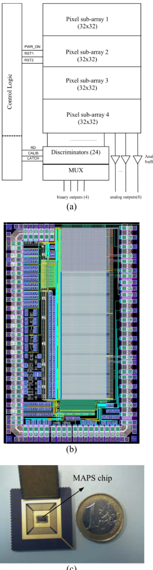
PWR_ON RST1 RST2 Pixel sub-array 1 (32x32) Pixel sub-array 2 (32x32) Pixel sub-array 3 (32x32) Pixel sub-array 4 (32x32) binary outputs (4) ……… … analog outputs(8) RD CALIB LATCH Analog buffers Discriminators (24) Co nt ro l L og ic MUX (a) (b) (c)
Fig. 3. a) Block diagram, b) layout and c) photography of the realized prototype chip.
The signal of the charge sensitive element is delivered to the amplifier via the series capacitance obtained by placing the polysilicon plate over the n-well area, as it is shown in Fig. 2b. The gate oxide is used providing a high value of the coupling capacitance. The signal is then amplified with a voltage gain about 15-20, aiming at total CVF about 150 µV/e-.
The principle of the direct AC coupling of the auto-reverse polarized charge sensitive element and the amplifier is shown in Fig. 2b. The choice of AC-coupling instead of DC-coupling allows independent bias of the input transistor in the amplifier from the potential settled on the n-well region during the detector operation. At the same time, the n-well diode is polarized with the maximum voltage available in the technology process bearing the optimization of the charge collection process. Since the second pixel does not use reset transistor for the diode, the CDS is used to extract the signal in subtraction from the reference level. The reference level for each new measurement is the state from the previous readout cycle.
III. ARCHITECTURE OF THE CHIP
A test chip was designed using a 0.25 µm CMOS digital process available through MOSIS. The chip consists of four sub-arrays of 32x32 pixels each, 24 column-level discriminators for signal sparsification, a fully programmable digital sequencer and output multiplexers for binary outputs, as it is shown in Fig. 3. The pixel pitch is 25 µm. The bottom three arrays contain the DC-coupling pixel type. The three arrays were designed aiming at different values of CVFs with different diode sizes. The first array from the top of the chip is built with the AC-coupling pixel type.
The chip readout is organized in columns processed in parallel. The first 24 columns are connected to discriminators, multiplexed onto 4 outputs. The last 8 columns of 32 are not connected to discriminators. Their analog outputs can be observed directly on the output pads. These direct outputs were used for testing of pixels with the results presented in the latter part of the paper. An additional output of the eights column of the group of columns with analog outputs allows to examine internal point of the amplifier before the clamping capacitance used for CDS processing.
The digital part includes two circuits. One is the digital control circuit, which is fully programmable and generates the patterns necessary for addressing, resetting and double sampling of the signals in pixels in a column parallel way. The rows are selected sequentially using a multiplexer every 16 clock cycles. The pattern is loaded to the chip serially during a programming phase at low frequency. The second circuit realizes a temporal multiplexing of the binary outputs signals (column discriminators) at a frequency value half that of the main clock frequency.
The design of comparators is based on an auto-zeroed amplifying stage and a dynamic latch, as it is shown in Fig. 4. They are an improved version of the previous design MIMOSA6 presented in [6][2]. The architecture was modified to use MOS capacitors instead poly-poly linear capacitors, because the fabrication process used does not feature this type of capacitors. To obtain a good linearity, a care had to be taken
to bias the capacitors in the accumulation regime. Level shifters before capacitors were used for this purpose. Thanks to the MOS capacitors, which have small dimensions, the size of the comparators is the same as the ones used in the previous design (220 µm x 25 µm).
The discriminators substract VRD from VCALIB for each pixel, and compare it with the reference differential voltage
2 1 Vref Vref Vref = − ∆ . C1 + _ C1’ + _ φ2 φ2 S1 S2 Vref1 Vref2 Vin S3 S4 φ1 φ1 VOS1 + _ φ1 S5 + _ φ1 S6 Latch VOS2 VOSL LA TC Q A1 A2 Q LATCH
Fig. 4. Bloc diagram of the offset compensated comparator.
IV. TEST RESULTS
Two kinds of measurements were performed on the chip. At the first step, the analog outputs were tested with a digital oscilloscope. The digital part generates a signal synchronized with the access to the first row of the pixel array. The analog signal from a single, selected column was examined using this synchronizing signal. It was possible to observe the signal of one single pixel in this way. During the tests with the oscilloscope, the clock operating frequency was of the order of 10 MHz, allowing clearly observing different phases (the first readout, reset of the charge collecting diode, reset of the clamping capacitance, second readout – calibration in the pixel access). At the latter step, measurements with main clock frequency of up to 100 MHz were also successfully performed. A thorough study of the analog outputs was made. The arrays of pixels with the DC-coupling were tested at the beginning as the basic option. The tests of the matrix containing pixels with AC coupling were also started. Experiencing some problems during the tests of AC-coupling pixels, the results of the DC-coupling option are presented in this paper only. The tests of the AC-coupling will be continued.
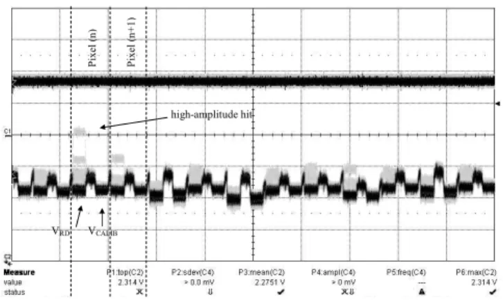
Fig. 5 shows the direct analog output signal observed. Note that the 2 levels for each pixel (VRD and VCALIB). The
black part is the pedestal and the grey lines correspond to the signal. The useful signal is the difference between these two levels. Tests without the source showed that the double sampling could eliminate offset dispersions of the in-pixel amplifying stage. The offset dispersions of the source follower output stage are to be corrected later by the column readout circuitry (discriminators). The two samples were recorded for each pixel and then subtracted offline, resulting in dispersions level less than 1 mV. The typical consumption of each pixel is reduced to 60 µA (the pixel dissipates only when it is powered-up). Pi xe l ( n) Pi xe l ( n+1 ) VRD VCALIB high-amplitude hit
Fig. 5. Output analog signal from 12 pixels of a column recorded on a scope (50 mV/div.). The useful signal for each pixel is the difference between these two levels, normally extracted by the column readout circuitry. A high-amplitude hit is clearly detected on pixel (n) during the read phase, corresponding to full energy deposition of the X photon. Other hits appear distinctly.
The ability to detect ionising radiation was tested with soft X ray photons from a 55Fe source in a second step. A 9.8 mCi
55Fe source was placed in the dark box at approximately 1 cm
of the chip with no material in between. After 15 minutes of the acquisition time, the hits could be seen on the oscilloscope as jumps on the output signal during the RD phase, as it is shown in Fig. 5 and 6. The conversion factors for different pixel architectures were grossly estimated from the maximum signal observed1. A good agreement comparing to ones
simulated was obtained. The conversion between the measured voltage and the charge collected by the diode was estimated knowing the energy of the photons from the source to be 5.9 keV for the dominating emission mode, corresponding roughly to 1600 e-. The knowledge of the CVF allows
estimating of noise, which does not exceed 20 e- ENC for the
worst case, i.e. the pixel with lowest CVF (@fCK=100 MHz
and with a measurement bandwidth of 200 MHz). The results obtained in this way can be only be considered as preliminary, allowing however demonstration of good ionising radiation detection capabilities, with low noise and low pixel-to-pixel DC level dispersion, of the new pixel architecture. The results obtained in tests are summarized in Table I.
The signal for an 55Fe source is higher than the one which
would be expected for a MIP (an average of 80 e-/µm x 6 µm =
480 e-), so the tests of the MIPs detection will be the next step
forward. The good signal to noise ratio shows MIP detection should be possible. Beam tests are expected to clarify this issue.
The binary outputs were all proved functional.
1 The calibration is done, assuming that maximum signal observed for the
exposition time correspond to the events of the photon impacts with conversion taking place in the n-well volume or in the depletion zone of the charge collecting diode, where the full quantity of the generated charge is collected within one pixel.
Pix el (n ) Pix el (n+ 1) VRD VCALIB
(a)
VRD VCALIB high-amplitude hits(b)
Fig. 6. Output analog signal from 32 pixels of a column recorded on a scope (20 mV/div.) a) with few small-amplitude hits, and b) with multiple high-amplitude hits.
V. CONCLUSIONS
The new method with series connection of the clamped capacitance used in the pixel design for double sampling enables the offset of each pixel to be literally eliminated. The prototype detector, consisting of 128 rows, can be read out and discriminated within 20µs with this design. Taking into account the temporal noise level and the residual FPN, the detection of MIPs should be possible using this technique. The small value of the residual pixel-to-pixel DC-level variation paves the way to the efficient on fly discrimination of signal during the readout of the detector, leading to the on-line data sparsification. The on-line sparsification is an issue for the layers L1 and L2 of the vertex detector in a future linear collider, where the high hit occupancy is expected. The feasibility of in-pixel double sampling with pre-amplification was successfully established. Implementation of the on chip analog to digital conversion and full data processing with digital hit reconstruction is still another future challenge.
The next step for the characterization of the chip will be to make statistical measurements on analog and binary outputs using a fast data acquisition system currently under development.
TABLE I
CHARACTERISTICS OF THE PIXEL AND THE READOUT ESTIMATED FROM
MEASUREMENTS Pixel
array
n° Sensing element
CVF
(µV/e-) Output RMS Noise @fCK=100 MHz Input Referred Noise (ENC) S/N* Pixel- to-Pixel FPN 1 self-biased n-well/p-epi diode (4.1 µm x 2.5 µm) 150** - - - - 2 n-well/p-epi diode (1.2 µm x 1.2 µm) 70 14 e - 120 3 n-well/p-epi diode (1.7 µm x 1.7 µm) 60 17 e - 100 4 n-well/p-epi diode (2.4 µm x 2.4 µm) 50 ~ 1 mV 20 e- 80 <1 mV
* The signal to noise ratio S/N was calculated using the maximum amplitude measured, divided by the rms noise voltage of the pixel.
** Simulation value, not yet tested.
VI. ACKNOWLEDGMENT
The authors are thankful to E. Delagnes, F. Lugiez, M. Rouger, all from DAPNIA/SEDI, and C. Colledani from LEPSI, for their help and advice.
VII. REFERENCES
[1] G. Deptuch, J.-D. Berst, G. Claus, C. Colledani, W. Dulinski, Y. Gornushkin, D. Husson, J.-L. Riester, and M. Winter, "Design and testing of monolithic active pixel sensors for charged particle tracking,"
IEEE Trans. Nucl. Sci., vol. 49, no. 2, April 2002, pp. 601-610.
[2] G. Deptuch, G. Claus, C. Colledani, Y. Degerli, W. Dulinski, N. Fourches, G. Gaycken, D. Grandjean, A. Himmi, C. Hu-Guo, P. Lutz, M. Rouger, I. Valin, and M. Winter, "Monolithic active pixel sensors with in-pixel double sampling operation and column-level discrimina-tion," IEEE Trans. Nucl. Sci., vol. 51, no. 5, October 2004, pp. 2313-2321.
[3] R. Merrill, "Intra-pixel reset noise cancellation," in Proc. 2001 IEEE
Workshop on Charge Coupled Devices and Advanced Image Sensors,
Lake Tahoe, Nevada, USA, June 2001, pp. 153-156.
[4] Y. Degerli, "Monolithic active pixels with in-pixel amplification and reset noise suppression for charged particle tracking in a 0.25µm digital CMOS process", preprint n° DAPNIA-04-184, CEA-Saclay/DAPNIA. [5] G. Deptuch, "Charge sensitive elements optimised for particle tracking,"
in Proc. 2003 IEEE Workshop on Charge Coupled Devices and
Advanced Image Sensors, Schloss Elmau, Elmau, Germany, 2003.
[6] Y. Degerli, N. Fourches, M. Rouger, and P. Lutz, "Low-power auto-zeroed high-speed comparator for the readout chain of a CMOS monolithic active pixel sensor based vertex detector," IEEE Trans. Nucl.