Design and Manufacturing of All-dielectric Optical
Metamaterial with Gradient Index of Refraction
by
Chih-Hung Hsieh
B.S., Power Mechanical Engineering,
National Tsing Hua University, Taiwan (2005)
S.M., Electronics Engineering
ARCHIES
MASSAcHMR'Err INSTITUTE OF VECHNOLOLGYJUL 3
0
2015
LIBRARIES
National Tsing Hua University, Taiwan (2007)
Submitted to the Department of Mechanical Engineering
in partial fulfillment of the requirements for the degree of
Doctor of Philosophy
at the
MASSACHUSETTS INSTITUTE OF TECHNOLOGY
June 2015
Massachusetts Institute of Technology 2015. All rights reserved.
Signature redacted
A u th or ...
...
Department of Mechanical Engineering
Signature redacted
March 6,
2015Certified by ...
George Barbastathis
Accepted by...
Profe
r of Mechanical Engineering
/ -A -2-Ie ipervisor
Signature redacted
David E. Hardt
Chairman, Department Committee on Graduate Theses
MITLibraries
77 Massachusetts Avenue Cambridge, MA 02139 http://Iibraries.mit.edu/ask
DISCLAIMER NOTICE
Due to the condition of the original material, there are unavoidable flaws in this reproduction. We have made every effort possible to provide you with the best copy available.
Thank you.
The images contained in this document are of the best quality available.
Design and Manufacturing of All-dielectric Optical
Metamaterial with Gradient Index of Refraction
by
Chih-Hung Hsieh
Submitted to the Department of Mechanical Engineering on March 6, 2015, in partial fulfillment of the
requirements for the degree of Doctor of Philosophy
Abstract
Gradient index (GRIN) materials offer the most general manipulation over wave fields of light compared to conventional refractive optics, where the light is deflected by the curved surface. The creative way to implementing GRIN optics is to construct a subwavelength structure with the electromagnetic characteristics that are unavailable via the natural material. This artificial GRIN structure also known as "metamaterial" can be classified into two general categories: film and slab GRIN optics, depending on the propagation direction of light penetrating through or propagating along the metamaterial.
In this dissertation, two different purposes of all-dielectric GRIN optics on (1) film: light extraction enhancement of the scintillator; (2) slab: aberration-free focus-ing usfocus-ing Lineburg lens, are both investigated. The scintillator made by ceramics like Lutetium Yttrium Orthosilicate (LYSO) possesses higher index of refraction at
1.82 than the surrounding environment, which causes extraction loss due to index
mismatching and total internal reflection (TIR) from scintillator to photodetector. A hybrid structure including two-dimensional photonic slab covered by the nanocone structure on the top was devised to recycle the energy loss from TIR and to create an index-matching layer in between. Design parameters of the hybrid structure were optimized by the simulation based on rigorous coupled-wave analysis, and the fabri-cation of hybrid structure was patterned by nanospheres (for nanocone structure) and laser interference (for photonic slab) lithography, respectively. Reactive ion etching (RIE) facilitated pattern transfer after two separate lithography processes. Finally, the characterization of nanostructured scintillator was performed with the ionizing source.
The rest of this research focuses on the implementation of the slab GRIN optics: Nanostructured Lfineburg lens. The Lineburg lens is an aberration-free lens that can perfectly focus light on the opposite edge of the lens area, and such property can be used for light coupling from fiber to waveguide in the Silicon photonics. We designed the nanostructured Lineburg lens on the silicon-on-insulator substrate using effec-tive index of refraction computed by photonic band theory, and the fabrication was
carried out by the e-beam lithography and RIE process. The device characterized by near-field scanning optical microscopy exhibited the single focusing behavior under fundamental mode illumination via the intensity map over the lens region. In addi-tion, the bi-foci phenomenon under higher order mode illumination was also revealed in the finite difference time domain simulation, and the ray picture for explaining the bi-foci was also included using Wigner distribution function and Hamiltonian ray-tracings.
Thesis Supervisor: George Barbastathis
4Signature
redacted
Acknowledgments
My favorite quote from Mahatma Ghandhi "First they ignore you, then they laugh
at you, then they fight with you, then you win" - is the best portrait of my entire
graduate life since I was still a research rookie in National Tsing Hua University. It
is a struggling period during the exploration of any research, and I could not have done this great accomplishment without the assistance from people working along
with me.
I would like to thank Prof. George Barbastathis for initializing my research life
at MIT. George offered me the opportunity to learn from his academic insight, and guided me through to break the ground I have not exposed to. He behaved as a strict teacher to insufficient aspects in my research, but always played as an attentive mentor for our need while pursuing the scientific truth. Working with George opens
up my vision of life.
I also thank Prof. Nicholas Xuanlai Fang and Karl Berggren for serving on my
committee. Nick always pulls me out by invaluable experience and suggestion when
I feel like sinking into the vortex of research puzzles. The discussion with Nick
enriches details of this thesis. Karl came to me for showing his abundant experience
on fabrication work, especially in demonstrating each process with a sound physical
ground instead of the black magic.
I would like to thank my lab mates in 3D optical system group. Dr. Lei Tian
is my best mentor in peers. Thoughts and reminders from him walk me through the challenge in my graduate life. Dr. Hanhong Gao sets a solid foundation for this
work with his brilliant work and help. Yi Liu accompanies with me for the tough time during research with her happy smile forever. Jeong-gil Kim is the best buddy
in preparing quals and defense. His discussion advances part of this work forward.
Justin Lee shares his MIT tips all the time. I would never forget the Thanksgiving
time we spent together. Dr. Hyungryul Choi and Dr. Se-Young Yang kindly showed me the basic skills and fruitful tricks to conduct a successful process in the fab. They instruct me the fabrication 101 in NSL. Dr. Nader Shaar gave me useful conversations
when I was lost halfway to my degree. I deeply appreciate his encouragement. Dr. Anthony Nichol surprised me by his entrepreneurship and his "great idea" on my first group presentation.
Strengths from the Taiwanese community held me up. Chia-Hsin Chen feeds me food and coffee to extend my energy on doing endless research load. We also definitely were the best partner in the basketball game. Jiun-Yih Kuan, Wei-Chun Hsu, and Miss Pan Pan and I not only gather for nice food and happy hour, but also engrave the unforgettable memory in our life. Yi-Heng Sen is the best consulting man when pursuing my future career. He taught me the secret in applying a job.
Special thanks to Dr. Yen-Sheng Lu and Dr. Chia-Ming Chang. Yen-Sheng played the role as my comrade-in-arms in NTHU and MIT. We've been collaborating over years, and continue our intersection in both future career. Chia-Ming was the man inspiring me for study abroad, and he is also the mentor who pass the ball to me for the buzzer-beat of my thesis.
Last, my sincere appreciation to my parents and my fiancee, Yunchia Liang. My parents, Huan-Hsu Hsieh and Chun-Mei Hsu raised me up in an austere and ordinary way but with their simple and correct philosophy. That's why I never deviate from the integrity. Yunchia came to me as an angel since I was 16 year-old. She stood with me through the challenges in my life. She never left from me whenever I need her. She's the one and the only one in my life.
Contents
1 Introduction
1.1 Gradient-index Metamaterials . . . . 1.2 Film gradient-index optics . . . .
1.3 Slab gradient-index optics . . . . 1.4 Thesis Architecture . . . .
2 Light Efficiency Enhancement of the Scintillator
2.1 Intorduction . . . . 2.1.1 Scintillation absorption and process 2.1.2 Light yield . . . .
2.1.3 Problem Definition . . . . 2.2 Structure design and optimization . . . . . 2.2.1 Hybrid Structure . . . . 2.2.2 Parameter optimization . . . . 2.3 Fabrication . . . .
2.3.1 Process flow . . . .
2.3.2 Langmuir-Blodgett Deposition . . .
2.3.3 Laser interference lithography . . . 2.3.4 Patterning results and Nanoimprint 2.4 Characterization . . . .
2.4.1 Principle of scintillation detector . 2.4.2 Measurement results . . . . 2.4.3 Discussion . . . . 21 22 23 24 27 29 . . . . 2 9 . . . . 29 . . . . 3 1 . . . . 3 2 . . . . 3 3 . . . . 3 3 . . . . 3 5 . . . . 3 9 . . . . 4 1 . . . . 4 3 . . . . 4 6 . . . . 4 8 . . . . 5 1 . . . . 5 1 . . . . 5 2 . . . . 5 3
2.5 Sum m ary . . . .
3 Implementation of Nanostructured Liineburg Lens 57
3.1 Introduction . . . . 57
3.2 Design and Simulation . . . . 60
3.2.1 Effective Index of Refraction of the Photonic Slab . . . . 60
3.2.2 Design Parameters and Structure Specifications . . . . 61
3.2.3 Sim ulation . . . . 63
3.2.4 Entire Device . . . . 64
3.3 Fabrication . . . . 66
3.3.1 Process Flow . . . . 66
3.3.2 Point Spread Function Measurement and Proximity Effect Cor-rection for Rod-slab LUneburg Pattern . . . . 67
3.3.3 Fabrication of hole-slab Luneburg lens . . . . 72
3.4 Characterization . . . . 74
3.5 Hamiltonian Ray-Tracing Results . . . . 77
3.5.1 High-order mode illumination . . . . 77
3.5.2 Wigner distribution function . . . . 79
3.5.3 Hamiltonian ray-tracing results . . . . 80
3.6 Sum m ary . . . . 82
4 Conclusions and future work 85 A List of Abbreviations 89 B Fabrication Summary 91 B.1 Surfactant Treatment of Nanospheres . . . . 91
B.2 Langmuir-Blodgett Deposition . . . . 92
B.3 Hybrid Structure Fabrication . . . . 95
B.4 Hybrid Structure Imprint . . . . 97
B.5 Point Spread Function Measurement for E-beam Writer . . . . 98
B.6 Fabrication of Rod-slab Linebug Lens . . . . 99 54
List of Figures
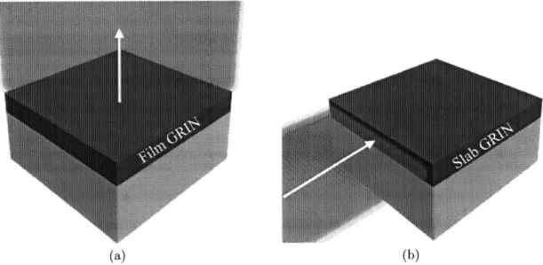
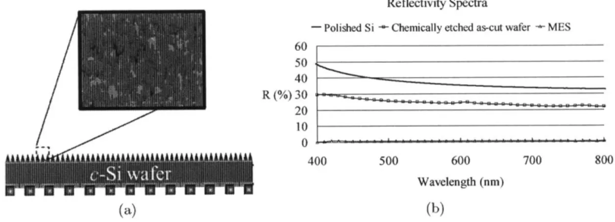
1-1 Two different categories of GRIN metamaterials (a) Slab GRIN (b) Film GRIN. The white arrows indicates the propagation direction of light. . . . . 22 1-2 Moth-eye structure (a) Application on an ultrathin monocrystal Si
solar cell (b) Reflectivity over visible band between 400-800 nm. . . . 23
1-3 Patterned sapphire structure for light extraction enhancement (a)
Pyra-mid [7] (b) Inverted pyraPyra-mid [8]. . . . . 24 1-4 Examples of GRIN lens (a) Maxwell's fish-eye lens (b) Lfineburg lens
(c) 1800 Eaton lens. Color lines denotes the ray path through the lens region . . . . 25 1-5 Flattened Lneburg lens for microwave frequencies (a) Fabricated 3D
lens (b) Index distribution along one vertical slice [9]. . . . . 26 1-6 Gradient-thickness Lineburg lens (a) Optical image of the fabricated
sample (b) Alignment results of light coupling from optical fiber to single-mode waveguide: with and without Lineburg lens [13] . . . . . 27 1-7 Plasmonic Lineburg lens (a) Device SEM. The PMMA layer with
gradient-thickness patterned by grey-scale e-beam lithography was de-posited on top of the gold layer (b) Experiment and simulation with different excitation conditions [14]. . . . . 27
2-1 Light extraction from Scintillator (a) Fabrication results from
[1].
[Note: RI denotes Refractive Index.] (b) The general usage of scintillator cou-pled with the PMT using the optical glue. . . . . 322-2 Three different hybrid structures sharing the photonic crystal as the backbone with the coverage of antireflective nanocones: Cone-cover, Cone-Topping, and Cone-Valley. . . . . 34
2-3 Angular distribution of emission photon inside the scintillator.
With-out any reflective wrapping, the photons escaping the scintillator from other facet of the crystal to the air causes the loss (white portion). In addition, part of the photon will be trapped until dissipation due to TIR (gray portion) [18]. . . . . 35
2-4 Number of the impinging photons simulated using Monte-Carlo method
by SLitrani for LYSO cylinder wrapping with teflon tape (a)
Imping-ing counts is function of the angle and recursion (b) Angular weightImping-ing function by summing up the data for each angle and normalized to the total count of the photons. . . . . 36
2-5 Verification of the approximation between cone and effective medium
on top of the photonic crystal using S4 simulation (a) Transmissivity
(b) Transmission probability. The simulation parameters: 500 nm in
pitch with 20% duty cycle. Thickness of the photonic crystal and cone are 500 and 350 nm, respectively. All schematics no to scale. . . . . . 38
2-6 Optimum of cone-topping case from the stack thickness 350nm and 150nm for photonic crystal and nanocone, respectively. . . . . 38
2-7 Optimization results with air or grease coupling (a) Cone-topping with
air (b) Cone-topping with grease (c) Cone-cover with air (d) Cone-cover with grease (e) Cone-valley with air (f) Cone-valley with grease. The performance ranking is Cone-topping > Cone-cover > Cone-Valley. . 40
2-8 Optimization results with grease coupling for ACW polymer (a)
2-9 Schematics of process flow. 100nm-big beads coating was carried out
by Langmuir-Blodgett method. Photonic crystals was defined by Laser
interference lithography after ARC and photoresist were spun on. Then sample went through three plasma etching: 15 minutes CF4 gas for
grating patterning, 5 minutes asher for resist removal, and another 5 minutes CF4 gas for nanocone patterning. . . . . 42
2-10 Working principle of the Langmuir-Blodgett trough. The compression bar can move isothermally to assemble the monolayer from floating beads [2]. . . . . 43 2-11 Langmuir-Blodgett method (a) Sensing principle of the Wilhelmy plate
[3]. (b) Three phases of monolayer: gas, liquid, and solid function of
the surface pressure [2]. . . . . 44 2-12 Results from Langmuir-Blodgett deposition on the glass slide.
Photo-graph at the left show blue reflection at coating area around 1" x 1".
SEM indicates the a monolayer assembled on the glass slide. . . . . . 45
2-13 Etching test of Si3N4 using silca beads as hard etching mask for (a) 0
(refrence) (b) 2.5 (c) 5 (d) 10 minutes in CF4 plasma. . . . . 46
2-14 Laser interference lithography (a) Principle of the laser interference lithography. The two beam coming from left and right interfered mu-tually to form the periodic fringes. (b) An example of exposure results using Lloyd's mirror. SEM showed the photoresist pattern with ARC layer underneath after development. . . . . 47
2-15 Fabrication results were shown by a series of SEM. First, the bead assembly on Si3N4 film was carried out by Langmuir-Blodgett method
followed by Laser interference lithography. Scallop sidewall on pho-toresist happened due to the thickness of the ARC is constrained by beads layer instead of the desirable value, but it did not affect the following RIE etching in CF4 plasma to pattern the photonic crystal.
Finally, the residual photoresist and ARC were removed by asher, and nanocones formed on top of the photonic crystal. . . . . 49
2-16 Characterization of the imprinted hybrid structure (a) Configuration.
Hybrid structure fabricated on ACW polymer by the counterpart 311RM on the fused silica imprinted from the silicon nitride mold. (b) 311RM curing by UV after filling up the gap between the Si3N4 mold and
fused silica. (c) The curing process of ACW polymer also uses the UV light with LYSO stamping. (d) and (e) both shows the imprinted re-sults of 31IRM polymer from cross-section and top-view, respectively. Imprinted 311RM becomes the counterpart of ACW that the main structure used for efficiency enhancement. . . . . 50
2-17 Operating principle of PhotoMultiplier Tube (PMT). PMT converts
the visible light to photoelectrons using photocathode, and photoelec-trons were amplified by several dynodes. Secondary elecphotoelec-trons from dynodes were collected by the anode and counted by the charge am-plifier. The output voltage from the charge amplifier was numbered
by analog-to-digital converter (ADC) for final output data. Therefore,
the channel number at multichannel analyzer (MCA) is proportional to the number of photoelectrons. . . . . 52
2-18 Light gain measurement. The peak of the channel number shifts to the
right from 378.1 to 395.4 after using the imprinted configuration of the hybrid structure with the same scintillator. . . . . 53
2-19 Intrinsic gain drop due to processes (a) Extraction loss by sample
heat-ing. The same annealing process as well as the deposition causes the extraction efficiency of the same LYSO crystal drop by 4.44% (b) Ab-sorption of silicon nitride film. A 11% transmission loss observed at the wavelength of 420 nm on the same crystal with and without Si3N4
coating indicates that the film quality should be tuned by controlling disposition parameters. . . . . 54
3-1 The concept of the nanostructured Liineburg lens consists of an array
of nanorods or nanoholes with varying diameter to control the effect index of refraction at each coordinate location. . . . . 58
3-2 Previous results of the nanostructued Lineburg lens devised using nano rod array based on the 2D assumption (1) Secondary electron micro-graph of the device (2) Characterization by near-field scanning optical microscopy. Note that the intensity contrast between focal spot and other places was only 0.05 [4]. . . . . 59
3-3 Nanostructued Lineburg lens using nanorod arrays (a) Effective
guid-ing medium (EGM) approximation of 2D finite height rod lattice struc-ture (b) Graphical solutions of wave guidance condition for transverse-magnetic polarization. Blue and red lines are the left and right hand sides of these equations, respectively. . . . . 59
3-4 Fundamental mode of the dispersion diagram for TE-like and TM-like polarization in 3D rod and hole structures. The nominal diameter of rods and holes are 0.2a and 0.9a, respectively. The grey patch denotes region of "leaky mode" defined by SiO2 light line, and the black dotted
line marks the desirable frequency. . . . . 61
3-5 All parameters used in MPB for the EIR computation. . . . . 62
3-6 The EIR library for constructing the nanostructured Lineburg lens in
both cases (a) Rod (b) Hole. . . . . 63
3-7 Schematics of nanostructured Liineburg lens constructed by nano hole
arrays. . . . . 64
3-8 Performance verification using MEEP for (a) Rod-slab lens (b)
Hole-slab lens. The black dotted line denotes the lens region, and the color at background overlaid with structure contour represents the E, field
3-9 Entire design for hole-slab Lineburg lens. The fundamental mode excitation with TM-like polarization is controlled by the dimension of the coupling waveguide. Bend waveguide prevents the stray light from
source fiber interfering with the evanescent wave over the lens region, and the tapered waveguide pertained the mode to lens region. . . . . 65 3-10 Process flow for rod-slab Lens (a) Pattern the device by e-beam
lithog-raphy on 6% HSQ (b) Etching device layer by RIE with gas combi-nation of BC13, and Cl2, and Ar (c) Deposition of silicon nitride by
PECVD for decreasing surface roughness scattering. . . . . 67 3-11 Process flow for hole-slab Lens (a) Pattern the device by e-beam
lithog-raphy on ZEP resist (b) Etching HSQ layer by RIE with CF4 plasma
(c) Etching the a-Si layer by ICP-RIE with SiCl4 and Ar plasma (d) Deposition of Si3N4 by PECVD for decreasing surface roughness scat-tering. . . . . 68 3-12 Proximity effect of e-beam lithography (a) Schematics for dose
distri-bution of isolated and dense patterns (b) Preliminary exposure results for rod-slab lens. . . . . 69 3-13 The measured PSF is denoted by the dose reciprocal function of the
radius of exposed rods, which is measured under the secondary electron m icroscopy. . . . . 70
3-14 Dose simulation for the rod-slab Lineburg lens using measured PSF to convolve with the pattern layout (a) without correction (b) with correction (c) Assigned dose map after correction. Enlarged pictures represents the rod at corner and center, respectively. . . . . 71 3-15 Proximity effect correction for rod-slab Liineburg pattern (a) on HSQ
(b) Transferred to a-Si. . . . . 71 3-16 Lithography results of hole-slab Liieburg pattern. The coupling, bend,
and tapered waveguide are all shown here. Holes around lens center are also clearly resolved without doing the PEC. . . . . 72
3-17 Etching results of hole-slab Lfieburg pattern. All components in the
design were successfully transferred to the device layer. . . . . 73 3-18 Modal analysis of wedge and rectangular waveguide. Cross-section
and their modes simulated by MPB were shown here for (a) Wedge (b) Rectangular waveguide, respectively. . . . . 73 3-19 The transmission check at the end of each device was performed by
Lumerical FDTD software. . . . . 74
3-20 Schematics of near-field scanning optical microscopy. . . . . 75 3-21 Modal analysis of wedge and rectangular waveguide. Cross-section
and their modes simulated by MPB were shown here for (a) Wedge (b) Rectangular waveguide, respectively. . . . . 75 3-22 NSOM results includes the topologcal (AFM) and optical (near-field)
information, and their combination for a 3D profiling (a) Bend waveg-uide (b) Part of tapered wavegwaveg-uide. . . . . 76 3-23 The modal analysis of rod-slab Lfineburg lens under different order of
illumination denoted by field plot (a) Fundamental (b) First (c) Second (d)Third mode. Fields from 2D simulation can approximate to the field at the center of the 3D slab. . . . . 77
3-24 The modal analysis of rod-slab Lineburg lens under different order of illumination denoted by intensity plot (a) Fundamental (b) First (c) Second (d)Third mode. Intensities from 2D simulation can approxi-mate to the intensity at the center of the 3D slab. . . . . 78 3-25 The Wigner distribution function computed for TM-like polarization
in rod-slab Lfineburg lens (a) Fundamental mode (b) The first mode (c) The second mode. Colorbar denoted at the side shared by three plots. . . . . 80 3-26 WDF change along with the nanostructured Lineburg lens. The WDF
undergoes the rotation (within lens) and shearing (after focusing) dur-ing the propagation. . . . . 81
3-27 Hamiltonian ray-tracing results with (a) Fundamental (b) Second-order
mode illumination. Rays with positive and negative radiances gener-ated from WDF at the source plane (left-hand side) propagate toward the lens to show the cancellation at focal point, which explains the bi-foci behavior in the high-order mode. Color bar at the right denotes the normalized general radiances. . . . . 82
B-1 Langmuir-Blodgett deposition (a) Isotherm plot for clean reference and a successful coating under pressure control (b) Multilayer results as-sembled on an Al-coated glass slide when the surface pressure at 20 m N / n . . . . 94 B-2 Optical property of the deposited Si3N4 (a) Dispersion (b) Extinction
coefficient over the spectrum. . . . . 96
B-3 Point spread function measurement of e-beam writer by imaging the exposed rod diameter (a) Dose at 58.8 pC (the 4 0th dot). Exposed dot fell down after development due to high aspect ratio (b) Dose at
11.8 piC (the 10 7th dot). The HSQ becomes a disk pattern due to the
List of Tables
2.1 Parameters for optimization. . . . . 36
2.2 Parameters for fabrication. . . . . 42
3.1 Specification summary of the nanostructured Lineburg lens at TM-like polarization. . . . . 63
Chapter 1
Introduction
Contents
1.1 Gradient-index Metamaterials ... ... 22
1.2 Film gradient-index optics . . . . 23
1.3 Slab gradient-index optics . . . . 24
1.4 Thesis Architecture . . . . 27
Gradient Index (GRIN) materials offer the most general possibilities for the manip-ulation of light. Applications of GRIN materials include focusing in imaging systems, guiding in optical fibers, light trapping structures for solar cells, light extraction from light emitting devices (LED), etc. Generally, these applications can be classified as two categories: film and slab GRIN optics, depending on the light that penetrates through or propagates along the GRIN medium.
In this dissertation, two devices from both categories were studied: (1) Surface engineering of the scintillator for light extraction enhancement (2) Nanostructured LUneburg lens implementation. In this chapter, a brief introduction to film and slab GRIN materials will be shown in the beginning followed by their problem definition in the ongoing sections. Last, the architecture of this dissertation will be discussed in the final section.
1.1
Gradient-index Metamaterials
The interaction between the light and medium strongly depends on the propagation direction of light as shown in Fig. 1-1, which will decide the way how to engineer-ing the material for GRIN purpose. Many GRIN applications require large variation of refractive index, so fabricating the structure around the scale of desirable wave-length would yield wider implementation margin than using traditional ion exchange or stuffing method in the fiber manufacturing. The novel device made by structuring natural materials to create the artificial electromagnetic characteristic is entitled with a name of "metamaterial" now because it hardly could be replaced with any other materials in nature. Benefits of GRIN metamaterials include better light retention due to all-dielectric implementation and compatibility with Si photonics system for coupling and processing of light. In general, the procedure of creating the GRIN metamaterial consists of (1) Analyze the index of refraction in the ambience around the device (2) Choose materials with proper index of refraction fit to the design re-quirement and fabrication process (3) Simulate and verify the performance of the GRIN metamaterial (4) Perform the fabrication (5) Characterize the GRIN metama-terial. Because of the difference between applications, the flow could be modified to
(a) (b)
Figure 1-1: Two different categories of GRIN metamaterials (a) Slab GRIN (b) Film GRIN. The white arrows indicates the propagation direction of light.
meet the implementation.
1.2
Film gradient-index optics
The film GRIN optics in this dissertation mainly represents applications for antireflec-tion and light extracantireflec-tion enhancement. They both penetrate the film through for the purpose of light collection but with opposite propagation direction. An optimum de-sign can not be used reversibly in this case due to index of refraction at emission point of light. When the light is going from low-index ambience to high-index substrate, the problem norinally tackles the impedance matching only. However, if the condition is reversed, i.e. the light is going from high-index substrate to low-index ambience, the total internal reflection (TIR) should be considered together with impedance match-ing for the light beyond the critical angle. One of antireflective applications is the light trapping structure for enhancing solar cell efficiency as shown in Fig. 1-2 [5, 6]. After nano-texturing the surface of the silicon substrate, the reflectivity can decrease down to 0.52% compared to the 25% of that results from traditional micro-texture. In addition, the nanocone structure also shows the same antireflection ability for large-angle incidence of light. However, the nanocone structure will not work out on the light extraction application due to TIR, so a different structure like diffractive grating
Reflectivity Spectra
60
5- Polished Si
+ Chemically
etched as-cut wafer
-MES 40 R (%) 30 10 10 0 400 500 600 700 800 Wavelength (nm) (a) (b)
Figure 1-2: Moth-eye structure (a) Application on an ultrathin monocrystal Si solar cell (b) Reflectivity over visible band between 400-800 nm.
is needed to break the TIR restriction. Take the case of light extraction from LED for instance. The light emitting layer is normally grown on the sapphire substrate with index of refraction around 1.8, which results in a critical angle of 34'. The light with incident angle beyond 34' will not be transmitted out from the sapphire, and is trapped to reflect back and forth within the substrate until energy dissipated. A photonic crystal as a two dimensional (2D) grating that is shown in Fig. 1-3 helps the extraction of light beyond critical angle [7, 8], but the trade-off is the less transmission for incident angle smaller than critical angle. Thus, a hybrid structure combining the antireflection for the light below critical angle and diffraction to break the TIR will be demonstrated in the chapter 2 of this dissertation.
1.3
Slab gradient-index optics
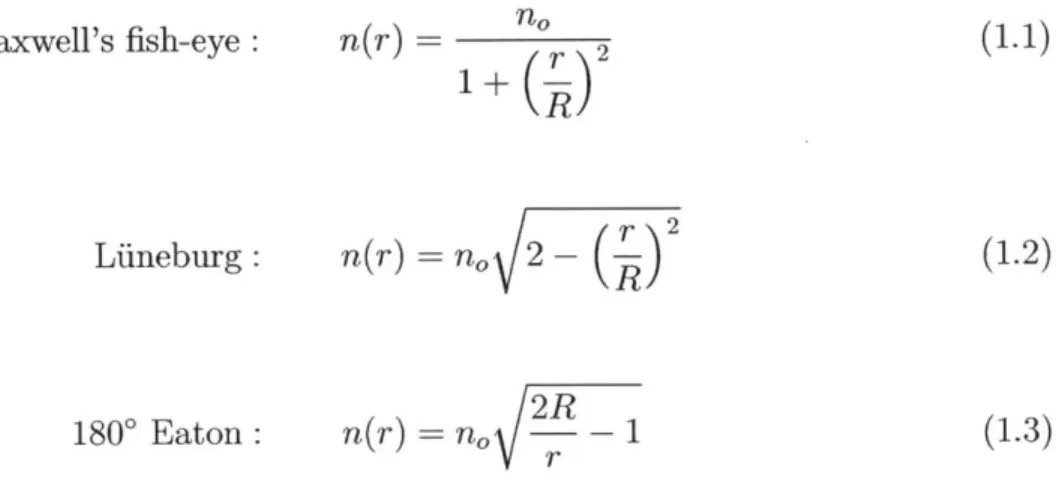
In slab GRIN optics, the light satisfying the guiding condition propagates along the waveguide for silicon photonics applications such as coupling and focusing. There are three famous and interesting examples of GRIN lens that have been studied well: Maxwell-fish eye, Lineburg, and Eaton lens as shown in Fig. 1-4. Here are their description of functionality: (1) Maxwell's fish-eye lens: If a point source is at the edge of the lens, those rays with direction pointing toward the lens region will focus right at the opposite edge again (2) Liineburg lens can perfectly focus the incoming
(a) (b)
Figure 1-3: Patterned sapphire structure for light extraction enhancement (a) Pyra-mid [7] (b) Inverted pyraPyra-mid [8].
plan wave from any direction to the opposite edge of the lens region (3) Eaton lens: the retro-reflector for bending the light with desirable degrees. The refractive index distribution of these GRIN lens follows:
Maxwell's fish-eye: Lineburg : 1800 Eaton: n(r) = n. 2 n(r) = 2 -(r)2 2R n(r) = n,, - -r r
where n, is ambient index of refraction outside the lens region, R is the radius of the lens region, and r is the radial polar coordinate with the lens center as origin. The Lineburg lens is the most applicable components in three of them because it has reasonable index variation in terms of fabrication and practical functionality. The benefit of Liineburg lens is omnidirectional focusing; however, exact implementation of this GRIN profile had, until recently, been available in microwave frequencies only for applications such as focusing into high-gain antennas [10, 9, 11]. People
con-(a) (b)
Figure 1-4: Examples of GRIN lens (a) Maxwell's
1800 Eaton lens. Color lines denotes the ray path
(c)
fish-eye lens (b) Liineburg lens (c) through the lens region.
(1.1)
(1.2)
trolled the index of refraction using layered material to build up the Lineburg lens in macro-scale. By exploiting nanolithography and fundamental understanding of refractive index manipulation through dispersion, infrared Liineburg lenses have also been successfully demonstrated. For example, Yao et al varied the thickness of the thin film to control the effective index of refraction (EIR) of the Lineburg lens, but the mode of the device becomes ill confined within the device layer due to relatively small thickness [12]. A recent example of gradient-thickness dielectric Lneburg lens using gray scale lithography by focus ion beam is shown in Figure 1-6 [13]. The same concept of using gradient-thickness dielectrics can be also applied to plasmonic Lineburg lens to create desirable mode index, but the intrinsic propagation loss from the metal surface is still incompatible with that in silicon photonics even using opti-cally pumped gain medium [14, 15]. The Lineburg lens is a great interface to mitigate the misalignment while coupling the light from a fiber to silicon photonics, but a de-sign that is compatible with current manufacturing of the silicon photonic system has not been fulfilled. Chapter 3 in this dissertation will demonstrate the process of implementing an Lineburg lens using the nanostructured film that is compatible to the current manufacturing of silicon photonics.
100 2 1.5 50 1 0 0.5 -100 -50 0 50 100 x (mm) (a) (b)
Figure 1-5: Flattened Liineburg lens for microwave frequencies (a) Fabricated 3D lens
1s -.--- -- ---- r--- - ---- -- -10 --- ---- ---- -9 --- --- --)Luneburg (1) wh a Luneburg (2) 0- - --- - - - -- .... -.Taper (1) 1.Taper (2) Alignment error (pm) (a) (b)
Figure 1-6: Gradient-thick L ine burg lens (a) Optical image of the fabricated sam-ple (b) Alignment results of light coupling from optical fiber to single-mode waveguide: with and without Lftneburg lens [13].
1.4
Thesis Architecture
Chapter 2 studies the hybrid structure for light extraction enhancement of the X-ray scintillator. This hybrid structure consist of a 2D photonic grating covered by nanocones. The optimization process utilizes rigorous coupled wave analysis for dif-ferent models at the design level because of the good approximation and relatively
(a) (b)
Figure 1-7: Plasmonic LUneburg lens (a) Device SEM. The PMMA layer with gradient-thickness patterned by grey-scale e-beam lithography was deposited on top of the gold layer (b) Experiment and simulation with different excitation conditions
shorter computation time compared to finite difference time domain simulation. By sweeping variables such as the periodicity and duty cycle of photonic gratings and the height of nanocones, the optimum for light extraction from different ambience can be determined. Results of the fabrication and characterization will also be summarized. An all-dielectric nanostructured Liineburg lens has not been presented completely including design, simulation, fabrication and characterization until the accomplish-ment in this work. Chapter 3 will introduce the work of nanostructured Liineburg lens carried out by other researchers previously from our group, and show the entire flow of implementation. Two design based on an array of nano rods and holes will be covered, and challenges resulting from the fabrication of the rod-slab case is also included. In addition, the near-field observation of nanostructured Lineburg lens is shown for the first time, and the analysis of the measured image using finite differ-ence time domain and Hamiltonian ray-tracing simulation are performed to explain characterization results.
Chapter 2
Light Efficiency Enhancement of
the Scintillator
Contents
2.1 Intorduction . . . . 29
2.2 Structure design and optimization . . . . 33
2.3 Fabrication ... ... . . . .. . . . .. 39
2.4 Characterization .... . .... .... ... .. ... ... ... 51
2.5 Summary ... ... ... . ... 54
2.1
Intorduction
2.1.1
Scintillation absorption and process
The ionizing radiation carries energy that can ionize the material including subatomic particles, ion, or atoms moving at relativistic speeds, and electromagnetic waves on the high energy end of the electromagnetic spectrum [16]. From the high energy physics, X-ray security, to positron emission tomography, plenty of applications rely on the scintillator to convert the ionizing radiation to non-ionizing radiation that is the feed for commercially available detector such as PhotoMultiplier Tube (PMT)
or Avalanche PhotoDetector (APD). The scintillator is a material that can emit the light by ionizing event happened inside the material after receiving ionizing radiation illumination. Mechanisms of the scintillation absorption consist of [1]:
" Heavy charged particles: the inelastic collision between impinging particles
at relativistic speed and the electrons of scintillator crystals can deposit the partial energy from the energetic particle to the local medium, which can be described by Bethe formula as [17]
dE 47ra2 [ 2mc23 2 2
dE In
-(2.1) dx mec2/32 [
(1- _2)
where the loss of total energy E along the penetration direction x within a homogeneous medium with a density of N atoms/cm3 and each atom of the atomic number Z is assumed here. I is an empirical constant and corresponds to the mean excitation and ionization potential of the scintillator. M is the rest mass of the particle, z is the particle charge, / is velocity (V =
#c)
and meand e are the rest mass of an electron and the electronic charge, respectively. For the non-relativistic case(3 < 1) the last two terms in the bracket can be neglected.
" Electrons: Impinging electrons with high energy (> MeV) deposit their energy
also in radiative form while they are deviated or deflected by the nuclei.
" Electronmagnetic radiation
1. Compton effect: an elastic collision between photon and a nearly free
electron inside the scintillator. The electron acquired the kinetic energy from recoil force or the impinging particle or high energy radiation.
2. Photoelectric effect: the photon was absorbed by a bound electron in
the inner shell of atom.
" Neutron: acquiring the energy from recoil force by the similar process with
Moreover, the scintillation process will involve aforementioned absorption resulting in re-emission at the visible band. When the impinging energy of particles or rays is larger than 100 keV, absorption happens in the inner shell (K or L shell) to generate the hole-electron pairs. The relaxation process of holes and electrons differs. The deep hole can be filled up by another electron in the atom to emit the light with a shallow hole generation, and the energetic electron within crystal, that is Auger electron, could also be generated during the relaxation. Both the radiative photon and Auger electron can generate the new hole-electron pairs until the energy of new electrons smaller than the ionization energy. Each relaxation of the electron-hole pair radiates a photon out, which provides the necessary conversion from ionizing to non-ionizing radiation.
2.1.2
Light yield
The conversion efficiency of the scintillation can be simply described as:
ph - Neh Nh
77 Np h x p = OSQ (2.2)
Neh,max Neh,max Neh
where the q represents the conversion efficiency of the scintillator. Nph and Neh,max
are the number of extracted photons, available e-h pair for conversion, maximum electron-hole pairs generated within the scintillator, respectively.
#
is e-h the con-version efficiency function of materials, namely Neh/Neh,max. S and Q indicate the energy transfer of e-h pairs and quantum efficiency of the luminescence center,re-spectively. The product of SQ is equal to Nph/Neh. In fact, a more powerful index for evaluating conversion efficiency is the light yield (LY), which is the total photon number generated per unit illumination energy. Using a series of simplification by
substituting other parameters, the absolute LY is expressed as [1]:
Lyabs = 0 (2.3)
Therefore, the LY is proportional to the total extracted photon number as well as the channel number of the multichannel analyzer, so it could be simply expressed by the peak variation of the channel number. More details about characterization and post-analysis will be discussed later.
2.1.3
Problem Definition
Light extraction from scintillators is one of the challenges in scintillator applications due to the relatively high refractive index of scintillators compared to the output environment. Total Internal Reflection (TIR) restricts the emitted light from scin-tillator that can couple out to the detector end. The same problem also happens in light extraction from light emitting device (LED) due to high index of refraction of the substrate. The solution to breaking the TIR usually utilizes a diffractive grat-ing, sometimes referred to as "photonic crystal", to diffract out the light beyond the critical angle. A. Knapitsch et al have facilitated the extraction efficiency by a 2D photonic crystal fabricated on lutetium oxyorthosilicate (LSO) crystal as shown in Figure 2-1(a) [18]. They patterned the Si3N4 deposited on top of the LSO substrate
10mm
500nm
(a) (b)
Figure 2-1: Light extraction from Scintillator (a) Fabrication results from [1]. [Note: RI denotes Refractive Index.] (b) The general usage of scintillator coupled with the PMT using the optical glue.
using e-beam lithography and reactive ion etching (RIE) because of the difficulty of directly plasma etching on scintillators and the refractive index of Si3N4 nearly
matching that of the scintillator. Results with optimized structure stack showed 56% gain of photon extraction while coupling the light from LSO to air. However, the scintillator is usually coupled with the PMT window using optical glue whose index is the same as the PMT window as shown in Fig. 2-1(b). The design for coupling light to air is not practical in applications.
Herein, the design of the structure should consider the refractive index at ex-traction plane as that in PMT window instead of air coupling. Moreover, a similar crystal compared to LSO, Cerium-doped Lutetium Yttrium Orthosilicate (LYSO:Ce), was used in this work as the substrate because of several advantages such as non-hygroscopic, high light output and density, quick decay time, and excellent energy resolution. Consequently, the hybrid structure combining the diffractive and antire-flective characteristics will be presented from design, optimization, fabrication and characterization based on LYSO crystals in the following sections.
2.2
Structure design and optimization
2.2.1
Hybrid Structure
The main idea of the hybrid structure is going to combine the benefit from antireflec-tive nanocones and diffracantireflec-tive photonic crystals. However, the two goals conflict in the sense that the first function (reducing Fresnel reflection) requires a subwavelength pitch, whereas the second function (diffracting light that would otherwise be TIRed) requires a diffractive structure with period bigger than wavelength. Fortunately, if the period is near the wavelength, a mix of both effects can be observed [19, 20, 21], and we can hope to balance them effectively to maximize light extraction. Because both benefits are not a pure addition in the optical performance, the design of exper-iment is adopted for evaluating the best performance. Basically, the hybrid structure uses a photonic crystal as the backbone with cover of nanocones array. Three
dif-ferent hybrid structures were depicted in Figure 2-2: cone-cover, cone-topping, and cone-valley. Physically, the photonic crystal backbone will keep the diffractive charac-teristic to break the TIR, and nanocones could be the index-matching layer between photonic crystal and environment. In order to save computation time, the parameter optimization is carried out by a free simulation software: Stanford Stratified Struc-ture Solver (S4) [22]. S4 is a frequency domain code to solve the linear Maxwells equations in layered periodic structures. Internally, it uses Rigorous Coupled Wave Analysis (RCWA; also called the Fourier Modal Method) and the S-matrix algorithm. S4 can compute the reflectivity, transmissivity, and diffraction efficiency in each order using transfer matrix method after layering the desirable design.
Photonic Slab
Cone-cover
Cone-Topping
Cone-Valley
Antireflective Cone
Figure 2-2: Three different hybrid structures sharing the photonic crystal as the backbone with the coverage of antireflective nanocones: Cone-cover, Cone-Topping, and Cone-Valley.
2.2.2
Parameter optimization
Before running the optimization, we need to consider the entire process from light emission to the extraction at exit plane. The light normally can be regarded as isotropic emission from the luminescence center if the scintillator is a homogeneous material. After emission, the light can bounce back and forth inside the scintillator if the incident angle is less than the critical angle. Hence, the probability of impinging photons on the extraction plane depends on the surrounding medium of the scintil-lator. Take the configuration of Fig.2-1(b) for example. The LYSO scintillator with refractive index of 1.82 is coupled to an optical glue with index of 1.41. One can simulate the angle distribution of impinging photons using freewares such as Geant4 and SLitrani based on the Monte Carlo method [23, 24]. Results as shown in Fig.
2-3 indicate only 28.9% of photons can be extracted directly or indirectly from the
extraction plane [18]. The rest of emission photons are leaked out to the air or dissi-pated due to trapping inside the scintillator by TIR. In order to recycle the photons impinging to other facets, a diffusive teflon wrapping or coating is usually used for surrounding medium to reflect most of the emission light from the side back to the
scintillator, whereas keeping the extraction plane clean for a good coupling.
The number of impinging photons for Air/LYSO interface as shown in the Fig. 2-4 was simulated by our collaborators in CERN (European Organization for Nuclear
511keV
gamrna
Figure 2-3: Angular distribution of emission photon inside the scintillator. Without any reflective wrapping, the photons escaping the scintillator from other facet of the crystal to the air causes the loss (white portion). In addition, part of the photon will be trapped until dissipation due to TIR (gray portion) [18].
p
-
direct into photodetector EM total reflection escapes crystal,J
no detection 'CC SSiimtator n=S.2 Simulated byS~ftra2000 0.025 1800 2000 160oo 0.02 1400 isoo 0.015 -1200 1000 1000 . 0.01-500 800 0 600 0.005 -400 5 670809 20G 60 200 0 10 20 30 40 50 60 70 80 90
Photon Numbers 15 30 Angle (degree) o Angle (degree)
(a) (b)
Figure 2-4: Number of the impinging photons simulated using Monte-Carlo method
by SLitrani for LYSO cylinder wrapping with teflon tape (a) Impinging counts is
function of the angle and recursion (b) Angular weighting function by summing up the data for each angle and normalized to the total count of the photons.
Research) using SLitrani for LYSO cylinder wrapping with teflon tape. In the simu-lation, 100,000 photons were randomly generated within the LYSO substrate at the beginning of the simulation, and SLitrani counted the number of photons hitting the extraction plane recursively until they were extracted or extinct. Obviously, most of the photons hit the extraction plane at the incident angle around 550 while using teflon wrapping. Evaluting the number of photon extraction along with on the distri-bution of impinging photons makes more sense to final results, but it has difficulty to integrate the SLitrani and S4 together for simulation in reality. Nontheless, the dis-tribution of impinging photons still can be used for optimization if two assumptions are made:
Table 2.1: Parameters for optimization. Constants
Si3N4 Index 2.06 LYSO Index 1.82
Parameters
Photonic crystal Nanocones
Period 100-3000 nm Period 100 nm
Duty Cycle 0-90% Thickness 50-350 nm
* The angular distribution of the impinging photons from the photonic crystal when coming back to the interface will have the same form as well as that in the grease (no structure) case. In fact, similar angular distribution of impinging photons for different medium at extraction plane remains in air and grease coupling as long as the teflon wrapping condition holds.
* The fraction of recuperated photons at each reflection on the extraction plane follows the similar pattern as well as that in the grease (no structure) case
(81.6%, 82.7%, 83.4%...). This argument is also sound because it was observed
that the angular distribution of the impinging photon strongly depends on the wrapping material instead of the medium surrounding the extraction plane.
In order to average out the variation between recurrences, the angular distribution of impinging photons could be summed up and normalized to get an angular weighting function, which is used with transmission data to compute efficiency maxima during the optimization.
Parameters affect the performance of the entire device were summarized in Table 2.1. The period of the nanocone was chosen as 100 nm that is fixed by the diameter of nanospheres in the fabrication. In addition, the definition of duty cycle remained the same as that in 1D case because it is more convenient to sweep the diameter instead of area linearly in the code. The other parameters were swept accordingly in the RCWA simulation to find the maximum of transmissivity. In S4 software, it is more effective to vary one periodicity per simulation, so the periodic nanocones will be accordingly replaced with an effective medium.
Thus, we need to verify this approximation before running through the whole optimization. The transmissivity of both cone and effective medium on top of a pho-tonic crystal have been simulated as shown in Figure 2-5(a). The result for cone case is consistent with that for effective medium except little underestimation while the incident angle is less than 150, but this variation could be neglected after considering the angular weighting of impinging photons as shown in Figure 2-5(b) due to low probability at around normal incidence. Herein, the entire process of optimization
0 0 0 .6 A
x
.2 0.8 10.6-OA 0.4 0.2 0 10 20 30 40 50 60 T-M 10 2D 30 40 50 -6 0 WA9OAA&l (deie) An&~ (depte)
(a) (b)
Figure 2-5: Verification of the approximation between cone and effective medium on top of the photonic crystal using S4 simulation (a) Transmissivity (b) Transmission probability. The simulation parameters: 500 nm in pitch with 20% duty cycle. Thick-ness of the photonic crystal and cone are 500 and 350 um, respectively. All schematics no to scale.
is to compute the efficiency gain compared to the bare Grease/LYSO interface and LYSO with photonic crystal. The duty cycle and pitch were swept for the specific thickness of photonic crystal and nanocone, respectively. An example of the result as shown in Figure 2-6 consists of the thickness of 150 and 350 rm for nanocone and
LEE LYSO-Grease Hybrid EffMed150 PhC350
a, 0 8 6 4 2 0 -2 -4 -6 -8 0.5 1 1.5 2 2.5 3 Pitch (p. m)
Figure 2-6: Optimum of cone-topping case from the stack thickness 350nm and 150nm for photonic crystal and nanocone, respectively.
a 00 aft
photonic crystal. After collecting all these optima, all efficiencies were depicted as shown in Figure 2-7 by their thickness compared to the Air/LYSO and Grease/LYSO interface, respectively. Furthermore, imprinting the hybrid structure is also one al-ternative, which is also simulated using the same process as shown in Figure 2-8. The available material ACW ( AC L2061-B, Addison Clear Wave Inc.) for nano imprint with refractive index at 1.67. In this case, we can have an additional polymer 311RM
(MINS-311RM, Minuta Technology) that has the similar index of refraction at 1.52 as
a buffer. This additional polymer also could be a good attachment between ACW and the fused silica substrate with index also at 1.5. The material property and imprint process will be discussed in the fabrication section.
As a result, we can choose the best parameters with compromise between the optical performance and fabrication feasibility to apply our structure on scintillator. Results show that the best design is the cone-topping case, and this is because it keeps the completeness of the photonic crystal for diffraction. The diffracted light from the crystal has good impedance matching from nanocones on top of the crystal. The cone-valley case has the worst results that support this argument. A careful proof could be obtained by analyzing the diffraction efficiency of each order using S4.
2.3
Fabrication
The fabrication of a hybrid structure using deposited silicon nitride is the motivation of this work because higher index margin for design and less material degradation compared to the polymer film. However, the process also brings additional issues to the final performance such as intrinsic gain loss by microcrack from deposition heating and absorption of silicon nitride due to inferior deposition condition. An imprinted scenario of hybrid structure was considered to be the better candidate for proof of concept eventually. More discussion about detrimental effects for directly processing the film with LYSO scintillator would be demonstrated in alternative message of this section.
Light Effcicy Enhancernent - Air 70 60-50 -LE Hybrid CH50rm 30P -LEE Hybrid CH100n -LEf HybdCH150am
20 -LEE Hybrid CH200am
-LEE Hybri CH250m
10 -LE LEE Hybrid CH350nmHybdd CH300nm
1P0 3-LEEC 6
i"0 50 35D 450 550 65D 75 PhC Thicknesw (nm)
(a)
Ught Efficiency Enhancement - Air
Light Efficiency Enhancement - Grease
-LEE Hybrid CH50n
-- dgdkkk -- LEE Hybrid CH100urn.
-LE y4rid CH15Mnm 8 6 4 0 150 250 350 450 550 PbC Thickness (um) (b) 9 8 7 6 4 3 1 250 350 460 550 650 750 PhC Thicimes (nn) (c)
Ught Efficiency Enhancement - Air
0 250 250 350 350 450 460 550 550 850660
PhC Thickness (nm) (e)
650 750
LUgit Efficiency Enhancemnt - Grease
-LEE Hybrid CH50nm
-LEE Hybrid CH100mm -- LEE Hybrid CH150om -LEE Hybrid CW20am -LEE Hybrid CH2VM=. -- LEE Hybrid CH300am
- -LEE Hybrid CHN350=m --- -LEEPhC 2~ 50 350 450 550 PhC Thickne (nm) (d) 8 6 650 750
-- LEE Hybrid CH50am -- LEE Hybrid CH10M= -LEE Hybrid CH150am -L.EEHybrid CH200am -LEE Hybrid CH250wm -LE Hybrid CH300nm -- LEE Hybrid CH350cm -IM -LEC 750 TSo 250 350 450 550 PhC Thickness (nm) (f) 650 750
Figure 2-7: Optimization results with air or grease coupling (a) Cone-topping with air (b) Cone-topping with grease (c) Cone-cover with air (d) Cone-cover with grease (e) Cone-valley with air (f) Cone-valley with grease. The performance ranking is Cone-topping > Cone-cover > Cone-Valley.
-LEE Hybrid CH200am
-- LEE Hybrid CU20M
-LEE Hybrid CH300=m -LEE Hybrid CH350am
--- LEE PhC 50 40 3 30 20 10 -LEE Hybrid CH50nm --- LEE Hybrd CHI00rwn
*LEE Hybrid CH150n
LEE Hybrid CH200nm. -LEE Hybrid CH250rn
- LEE Hybrid CH3sOnm -LEE Hybrd CH350 n - -LEE hC 40 W30 10 -LEE Hybrid CH50nm
-- LEE Hybrid CHI00rn -- LEE Hybdid CHI150rn -- LEE Hybrid CH200rn -LEE Hybrid CH250rn y EEHbdd CH300rn -LEE Hybrid CH350fnm - -LEE PhC 50 2 0
5 6
L- -LEE Hybrid CU50m
2-LEE -LEE Hybrid Hybrid C2M CH25om, 9 -LEE -LE Hybrid CH200mHybrid CH250am
-.-LEE HybriCHWM -LEE Hybrid CH300am
-LEE Hybrid CH350am -LIBE Hybrid CH350am
- -LEE P0C ACW -* -LEE PhC ACW
35.0 4 5 65D 750 250 35D 450 550 650 750
Pb cks. (m> PbCa Tbcnew (.m>
(a) (b)
ight Efficiency Enhancemet -Grefte
6.
5,
LEE Hybr C3M
3
I
LI Hybrid CH100mLEE Hybrid CHI50no
2 -Lim HybridCH2i --LEE Hybri CH250=m I ~-LEE Hybrid CH300nm. --LEE Hybri CH350=m --LEE PC ACW 50 250 350 450 6 75 bc kse .. (em> (c)
Figure 2-8: Optimization results with grease coupling for ACW polymer (a) Cone-topping (b) Cone-cover (c) Cone-valley.
2.3.1
Process flow
In the previous section, we found the optimum for each case, and the cone-topping hybrid structure yields the best result among three scenarios. Simulation results indicate that parameters for the best efficiency gain at 68.5% consist of 300/700 nm for cone/grating stack. However, this requirement needs a durable hard mask that is hardly achieved in nanosphere lithography available in our lab. Thus, another optimum was needed for fabrication feasibility. Fortunately, another parameter set consisting of 150/300 nm for cone/grating stack with 600 nm periodicity and 10% duty cycle yields an acceptable efficiency gain at 64.5%. However, the LYSO substrate is implicitly not appropriate for directly processing. More details are discussed in
II Ii* . I
_& LihEfrkciency Enhmncment - Grems U&g Efficiency Enacwt- Gtusw
Table 2.2: Parameters for fabrication. Parameters
Photonic crystal Nanocones
Period 1100 nm Period 100 nm
Duty Cycle 10% Thickness 150 nm
Thickness 350 nm
alternative message section of this chapter. The imprinted hybrid structure is used in the following process. The summary of the chosen parameters were shown in Table 2.2.
The entire process flow is depicted in Figure 2-9. First, a 500nm-thick Si3N4
layer was deposited on Si substrate using plasma enhanced chemical vapor deposition
LB Deposition
Interference Lithography
PhC Structuring
4
Cone Forming
Resist Ash
Figure 2-9: Schematics of process flow. 100nm-big beads coating was carried out
by Langmuir-Blodgett method. Photonic crystals was defined by Laser interference
lithography after ARC and photoresist were spun on. Then sample went through three plasma etching: 15 minutes CF4 gas for grating patterning, 5 minutes asher for