Nanoscale
Analysis by EFTEM and FIB-Tomography for Optimization of Thin-Film
Silicon Solar Cells
D.T.L. Alexander,* S. Nicolay,** P. Cuony,** M. Cantoni,* and C. Ballif**
* Centre Interdisciplinaire de Microscopie Électronique (CIME), École Polytechnique Fédérale de Lausanne (EPFL), Lausanne, CH-1015, Switzerland
** Institute of Microengineering (IMT), École Polytechnique Fédérale de Lausanne (EPFL), Neuchâtel, CH-2000, Switzerland
To produce high-efficiency thin-film Si micromorph (tandem of amorphous and microcrystalline junction) cells requires optimization of all thin-film components. To this aim, we high-light the contribution of advanced electron microscopy to the optimization of plasma-enhanced chemical vapor deposition (PE-CVD) SiOx and low-pressure (LP-) CVD ZnO layers for micromorph cells. The PE-CVD SiOx films are used as intermediate reflectors, combining desireable properties of a low refractive index for minimal light absorption, with a high transplanar, but low in-plane, conductivity to channel current between the two junctions [1]. Although known to be a composite of conductive Si nanoparticles (Si NPs) in an insulating SiO2 matrix, the microstructure giving their particular conductivity properties was previously unknown. Now, cross-section energy-filtered (EF-) TEM imaging of test films finds that the Si NPs grow in branched/dendritic networks that connect the two surfaces of the films, producing transplanar conductive routes, as shown in Fig. 1a. The image is taken with an Ω-filter on a JEOL 2200FS, using a 4 eV window centred on the 17.5 eV Si plasmon peak. NP definition is improved by removing the intensity contribution from the broad SiO2 plasmon peak. This is done by adapting the STEM-EELS approach of Schamm et al. [2] to EFTEM, using a linear fit between 10 and 23 eV filtered images to model, and then subtract, the SiO2 intensity contribution. Extension of the analysis to more cell-like conditions of growth on pyramidal ZnO shows that the conductive transplanar networks are maintained, but that their formation and connectivity clearly depends on the underlying ZnO morphology [Fig. 1b].
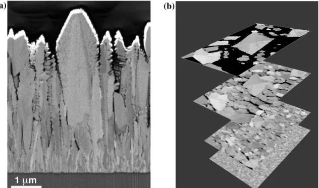
The pyramidal ZnO structures shown in Fig. 1b are used as transparent conductive oxide layers, and play an essential role in scattering light into the junctions to increase cell efficiency. In order to optimize the growth of such surface architectures, their formation, which begins with competitive growth of randomly-oriented nanocrystalline nuclei on an amorphous glass substrate, must be understood [3]. Being non-epitaxial, the films have complex grain structures that are challenging to analyse. However, we find that FIB-SEM cross-section imaging of the films with a Zeiss NVision 40 provides an excellent tool for their analysis. By using a 1.5 kV electron beam, and an in-lens backscattered-electron detector, grains < 20 nm in diameter can be distinguished with a contrast superior to BF or DF TEM imaging (Fig. 2a). Slice-and-view tomography extends this approach to the third dimension. Fig. 2b shows a small portion of data from such an acquisition for a ZnO test film, with a basic voxel size of 10 x 10 x 10 nm. The transition from high nucleation density to grain grain coarsening, driven by competitive growth, is clear. Such a data set provides extensive scope for analysis. For instance, by correlating with XRD data, we know that the pyramids of this film are oriented parallel to [110]. Now, the FIB data shows that they grow with 2-fold rotational symmetry around axial twin planes (Fig. 2b). TEM studies are underway to investigate the growth axes of such ZnO films more deeply, along with identifying the crystallinity of the Si NPs in the SiOx films.
1336
doi:10.1017/S1431927610057156 © Microscopy Society of America 2010Microsc. Microanal. 16 (Suppl 2), 2010
https://doi.org/10.1017/S1431927610057156
References
[1] Buehlmann et al., Appl. Phys. Lett., 91 (2007) 143505. [2] Schamm et al., Ultramicroscopy, 108 (2008) 346. [3] Nicolay et al., Cryst. Growth Design, 9 (2009) 4957.
[4] The Swiss Federal Office for Energy (OFEN) is acknowledged for financial support.
FIG. 1. Cross-section EFTEM images of Si NPs in SiOx films made on flat Si wafer (a) and on pyramidal ZnO (b). Branched/dendritic conductive pathways of Si NPs cross the films.
FIG. 2. FIB-SEM cross-section grain structure image of a ZnO test film (a); compared to typical pyramidal ZnO for cells, its unusual structure results from very non-standard LP-CVD conditions for growth studies. Lateral slices of tomographic data from the same region (b). Rotational symmetry seen around an axial twin plane in the central pyramid is not visible in one cross-section alone.
(a) (b)
(a) (b)
Microsc. Microanal. 16 (Suppl 2), 2010 1337
https://doi.org/10.1017/S1431927610057156