HAL Id: hal-02875603
https://hal.archives-ouvertes.fr/hal-02875603
Submitted on 10 Dec 2020
HAL is a multi-disciplinary open access
archive for the deposit and dissemination of
sci-entific research documents, whether they are
pub-lished or not. The documents may come from
teaching and research institutions in France or
abroad, or from public or private research centers.
L’archive ouverte pluridisciplinaire HAL, est
destinée au dépôt et à la diffusion de documents
scientifiques de niveau recherche, publiés ou non,
émanant des établissements d’enseignement et de
recherche français ou étrangers, des laboratoires
publics ou privés.
thin films through nanopatterning
Jeff Nyalosaso, Audrey Potdevin, François Réveret, Pierre Disseix, Rachid
Mahiou, Geneviève Chadeyron
To cite this version:
Jeff Nyalosaso, Audrey Potdevin, François Réveret, Pierre Disseix, Rachid Mahiou, et al..
Enhance-ment of light extraction in Y3Al5O12:Tb3+ thin films through nanopatterning. Chemical Engineering
Science, Elsevier, 2020, 213, pp.115416. �10.1016/j.ces.2019.115416�. �hal-02875603�
UNCORRECTED
PROOF
Chemical Engineering Science xxx (xxxx) 115416 Contents lists available at ScienceDirect
Chemical Engineering Science
journal homepage: http://ees.elsevier.com
Enhancement of light extraction in Y
3
Al
5
O
12
:Tb
3+
thin films through nanopatterning
Jeff L. Nyalosaso
a, Audrey Potdevin
a, François Réveret
b, Pierre Disseix
b, Rachid Mahiou
a,
Geneviève Chadeyron
aaUniversité Clermont Auvergne, CNRS, SIGMA Clermont, ICCF, F-63000 Clermont–Ferrand, France bUniversité Clermont Auvergne, CNRS, SIGMA Clermont, Institut Pascal, F-63000 Clermont–Ferrand, France
A R T I C L E I N F O
Article history:Received 23 September 2019
Received in revised form 21 November 2019 Accepted 3 December 2019 Available online xxx Keywords Sol–gel process Langmuir-Blodgett LEDs Surface nanostructuring Light extraction
A B S T R A C T
Light extraction is a key parameter to improve the performances of optical devices. Nanopatterned Y3Al5O12:Tb3+luminescent coatings usable in such devices have been elaborated and have shown enhanced
emission efficiency compared to their unpatterned counterparts. These nanostructured films were obtained by using the colloidal lithography combined with the Langmuir-Blodgett technique. It is the first time to our knowl-edge that this patterning technique is directly applied on YAG matrix. Resulting nanostructuring is a hexagonal network capable of modifying the light travelling path within the substrate. Conventional and angular-resolved photoluminescence were investigated on both unpatterned and patterned samples. Due to the nanostructuring, the extraction efficiency is improved by 26% and 131% depending on the crystallinity of the sample. Noticeably, nanostructuring is found to have an influence on the angular distribution of photoluminescence whose intensity has been evaluated to its maximum normal to the film surface.
© 2019
1. Introduction
Developing high efficiency White Light-Emitting Diodes (WLEDs) for different optical applications such as displays and lighting devices has been a topic of interest for several years. WLEDs generally com-bine a semiconductor chip emitting in the ultraviolet or blue wave-length region to one or more phosphor(s) deposited in the form of coat-ings usually using either on-chip or remote configurations. (Khanna, 2014; McKittrick and Shea-Rohwer, 2014; Piquette et al., 2016) Even if actually commercialized LEDs-based display and lighting devices are characterized by good photometric parameters, their optical perfor-mances can be further improved notably their luminous efficacy. (Geng et al., 2014; Khan et al., 2019) One of the factors we can act on is the Light Extraction Efficiency (LEE), which represents the ratio be-tween the number of photons extracted to the air and the number of photons generated in the active layer. (Geng et al., 2014; Lenef et al., 2018; Narendran et al., 2005; Tian et al., 2018) Actually, the emitted light is hard to extract into the air since there is a gap between the high refractive index of the phosphor (n ~ 1.8 for the most com-mon used Y3Al5O12:Ce3+phosphor) and the air (n ~ 1). Total internal
reflection (TIR) thus occurs and a large fraction of the light produced in LED devices is backscattered to the chip or trapped in dielectric struc-tures inherent to the substrate (luminescent coatings).(Lenef et al.,
E-mail address: audrey.potdevin@sigma-clermont.fr (A. Potdevin)
2018; Zhmakin, 2011) The trapped light is then, either emitted from the substrate edge or re-absorbed then converted to heat, which entails in both cases the decrease in forward light emission, limiting the LEE value. The key to increase the escape probability of photons and so on LEE value, is to give them more chances to find the escape cone de-fined by , nairand nALbeing refractive indexes of the air
and of the Active Layer (AL) (for example the phosphor) respectively. (Kim et al., 2016; Sun et al., 2016) It can occur either by angu-lar randomization of photons by scattering them from a structured sur-face(Kim et al., 2016; Kumar et al., 2011; Schnitzer et al., 1993; Sun et al., 2016) or by using an intermediate layer with an appropri-ate refractive index between the AL and the air. (Fang et al., 2013; Khan et al., 2019) In both cases, TIR will be attenuated and LEE value will increase which has been demonstrated on LED chips. (Geng et al., 2014) Among the existing light extraction management strategies based on these principles, one can cite surface roughening (roughened or cor-rugated substrates) (Kim et al., 2016; Sohn et al., 2004; Youn et al., 2015), photonic crystals(Devys et al., 2014), nanorods or nanopil-lars(Ding et al., 2017; Yang et al., 2014) and many others. In order to reduce the waveguide effect and consequently to optimize the for-ward light extraction, we have chosen to directly structure the surface of a thin phosphor layer into a hexagonal network at the nanometric scale. The surface nanostructuring of luminescent phosphor coatings has been widely investigated by several research groups in recent years. By replacing the luminescent coatings currently used in LED devices with https://doi.org/10.1016/j.ces.2019.115416
UNCORRECTED
PROOF
nanostructured coatings, it was thus expected to improve the perfor-mances of the LEDs lighting devices while maintaining or even reduc-ing their cost. The reported works concerned not only the field of LED lighting but also that of displays for which surface structuration leads to better resolution of screens for example. In this context, different types of phosphors have been studied: organic (europium chelates(Devys et al., 2014; Revaux et al., 2011)) or inorganic (mainly sesquioxides of Y2O3: RE3+− RE = Er, Eu (Sohn et al., 2004) or Gd2O3:Eu3+types
(Do et al., 2005), but also sulfides (Ko et al., 2008) and more recently the YAG:Ce matrix (Cho et al., 2014; Ge et al., 2015; Gorsky et al., 2018; Park et al., 2012; Sun et al., 2016; Wang et al., 2016a)). As an example, Gorsky et al. 2018 recently measured a peak extraction enhancement by a factor of 2 from YAG:Ce converters patterned with TiO2nanodisks compared to a flat reference. Among existing literature,
only Wang et al. 2016a reported a direct micropatterning of the YAG matrix, using a short-pulse laser (microwells array with spacing between adjacent microwells around 7 µm). Indeed, due to its high mechanical strength and excellent chemical stability, YAG matrix is very harsh to pattern directly regardless of the method. Consequently, main works in-tended for enhancing forward YAG:Ce3+emission involve the use of
for-eign materials such as SiO2, TiO2or SiNx. (Cho et al., 2014; Ge et al.,
2015) The durability of these structures is not well known because they could be deteriorated or delaminated from the phosphor surface over time notably under operating conditions.
In this work, we explore a simple surface patterning strategy that we have carried out specifically on YAG matrix-based coatings for the pur-pose of enhancing their luminescence performances. This strategy repre-sents an innovation insofar it allows directly structuring any kind of ox-ides or fluorox-ides available through the sol-gel process. In this way, it in-volves both colloidal lithography and Langmuir-Blodgett technique (LB). This approach relies on the self-assembly of a monolayer of beads of a given diameter on a substrate. These beads are generally silica nanos-pheres, polystyrene or PMMA (Vogel et al., 2015) and the substrate may be bare or already coated with the selected material of interest. The monolayer of beads then serves as a physical mask. (Ai et al., 2017; Vogel et al., 2012) The material to be structured is deposited on this mask by physical techniques [Physical vapor deposition (PVD)] or chemical way (impregnation) so as to partially or completely fill the interstices that are formed between the beads. The monolayer of beads is then removed (by heating, ultrasound or washing) leaving a periodic structure of the selected material. This technique has already been used successfully to improve the efficiency of blue LEDs by structuring the sil-icon wafer or the GaN chip. (Geng et al., 2014)
Obtaining a good quality network obviously involves checking the homogeneity of the (mono)layer(s) of beads. Different deposition tech-niques have been used and reported in the literature. (Liang et al., 2019; Vogel et al., 2015) Among them, “floating-transfer” and spin-coating techniques seem to be the most convenient to implement. (Colson et al., 2011; Lee et al., 2007; Vogel et al., 2012) How-ever, in our work, the technique of Langmuir-Blodgett was favored to achieve monolayers of polystyrene nanospheres (NPS). The LB process, which was first used as an efficient technique for the assembly of mol-ecular monolayers, relies on the controlled compression of monolayers consisting of amphiphilic compounds located at the water / air inter-face. (Bardosova et al., 2010; Ulman, 2013) A substrate, generally treated to be hydrophilic and initially immersed in water, is gently re-moved from this water subphase while the amphiphilic molecules ad-here to its surface under the effect of pressure exerted by the barri-ers of the LB system. Today, this technique has the great advantage of controlling the number of deposited layers by varying the number of “soak-withdrawal” cycles of the substrate (Tian et al., 2018). It is also very robust (very good reproducibility) (Reculusa and Ravaine, 2003) and can be used to cover large surfaces with compact assemblies of par
ticles. (Colson et al., 2013; Vogel et al., 2015) Despite these ben-efits, there is little research on the use of the LB technique to perform “NanoSphere Lithography” (NSL) (Bardosova et al., 2010) and most of them are dated after 2010.(Szabó et al., 2013; Wang et al., 2016b) In our work, a mask based on a monolayer of polystyrene nanoparticles was used and deposited by the technique of LB on sol-gel derived coat-ings, after having optimized all the parameters of LB deposition.
Sol-gel chemistry has proved to be a very efficient method for the production of thin layers of oxides on different types of substrates. (Brinker and Scherer, 2013) In the field of optics, this method offers the possibility of controlling the density of the deposited films and con-sequently their refractive index. (Akaltun et al., 2011; Mergel et al., 2000) It also promotes in particular a better dispersion of the optically active centers (rare-earth ions for example) in inorganic or composite dielectric matrices. (Brinker and Scherer, 2013; Shionoya, 1998) In our study, we used a sol-gel process developed in-house (Potdevin et al., 2006a; Potdevin et al., 2009) to elaborate luminescent amor-phous and crystallized Y3Al5O12:Tb3+(YAG:Tb) coatings. This phosphor
and derived Tb3+doped garnets have been shown to possess
interest-ing features for solid-state lightinterest-ing devices. (Potdevin et al., 2010b) Furthermore, this study is used as a proof of concept to investigate the influence of nanostructuring of sol-gel derived thin films on their light extraction efficiency and on their angle-dependent light emission. The morphological and structural properties of the films were studied using standard methods (AFM, SEM, XRD) at each step of the nanostructuring process, when necessary. Then, the photoluminescence measurements were carried out in order to determine the influence of the nanostruc-turing on the light extraction efficiency.
2. Material and methods
2.1. Preparation processes
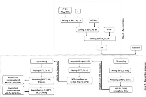
The nanopatterning process is schematized in Fig. 1.
2.1.1. Preparation of the YAG:Tb sol (step 1)
YAG:Tb (20%) precursor sol was prepared by using the sol-gel method, following a process already described in the literature. (Pot-devin et al., 2006a, b) In this preparation, anhydrous yttrium and ter-bium chlorides (YCl3and TbCl3, 99.9% purity, Sigma-Aldrich) and
alu-minum isopropoxide (Al(OiPr)3, ≥98% purity, Sigma-Aldrich) were used
as precursors for sol-gel reaction. First, YCl3and TbCl3were dissolved
in isopropanol under argon atmosphere. Atomic ratio [Tb3+/(Y3++
Tb3+)] in the YAG:Tb sol was set to 20 mol% since this doping rate
has been determined to lead to the best optical properties upon blue or UV radiation. (Potdevin et al., 2006b) After complete dissolution of YCl3and TbCl3, potassium chunks (K, 98% purity in mineral oil,
Sigma-Aldrich) were added to the reaction mixture at 85 °C so that to initiate sol-gel reaction. A KCl white precipitate was directly observed. Al(OiPr)3was added directly after 1 h reflux. After two more hours of
re-flux, the sol was stabilized by acetylacetone (acacH, 99% purity, Merck) used as a chelating agent. Indeed, it forms stable complexes when mixed with Tb3+, Al3+and Y3+ions. (Potdevin et al., 2016) The final molar
composition of the reaction mixture was 1 Tb : 4 Y : 5 Al : 9 K : 5 acacH. The KCl precipitate was separated from the sol by centrifugation.
2.1.2. Preparation of the YAG:Tb films (step 2)
Spray-coating, spin-coating and dip-coating are among various meth-ods that exist for depositing phosphors thin films. (Brinker and Scherer, 2013; Potdevin et al., 2009; Shionoya, 1998) Under the experimental conditions developed during our work, the two first methods of deposition did not provide a smooth and even film sur-face. Spin-coating method led to irregular dense films with
UNCORRECTED
PROOF
J.L. Nyalosaso et al. / Chemical Engineering Science xxx (xxxx) 115416 3
Fig. 1. Sol-gel and deposition processes of YAG:Tb (20%) nanostructured thin films.
whereas spray-coating method generally leads to films characterized by a very rough surface. (Potdevin et al., 2006a; Potdevin et al., 2011) The dip-coating method has been chosen for its simplicity and efficiency. This method offered optical quality coatings with easily con-trollable thicknesses and good surface homogeneity. The YAG:Tb amor-phous films obtained from this method have all a smooth and homoge-neous microcracks-free surface. (Potdevin et al., 2009) In our process, previously prepared YAG:Tb sol (actually, YAG:Tb precursor) was de-posited by dip-coating on quartz slides in order to form a first amor-phous coating (sublayer) of YAG:Tb, further annealed at 400 °C. It has been demonstrated that the intensity of photoluminescence (PL) is de-pendent in particular on the thickness of the coating. (Cho et al., 2007) Based on our previous work, (Potdevin et al., 2009) we chose to prepare films enough thick to have significant PL efficiency; hence we worked with a coating of 1 μm which represents a good compromise be-tween the PL efficiency and a reasonable number of layers (see Fig. S1 which evidences the film thickness). Indeed, in the used deposition con-ditions, such a thickness required 20 cycles of dip-coating with a concen-trated sol of YAG:Tb(20 mol%). This concentration results in a weakly viscous sol but allows avoiding delamination phenomenon which gener-ally occurs if the thickness of each coating is too important. The ther-mal annealing process we used has been optimized to lead to homoge-neous thin films free of cracks (necessary condition to have a subsequent PS beads deposition of best quality). Actually, this step has to be mas-tered to avoid microcracks which are the consequence of the difference in thermal expansion coefficients between the quartz substrate and the YAG: Tb film. (Cho et al., 2007)
It is on this first amorphous YAG:Tb coating (sublayer) that the colloidal lithography involving the polystyrene (PS) NPs of 460 nm (NPS-460, 10%, Sigma-Aldrich) was carried out. This method consisted in depositing by the LB technique (with a Kibron MicroTroughXS® sys-tem) a compact monolayer of NPS on the amorphous layer of YAG:Tb. Consecutively, a very small quantity of YAG:Tb sol (several hundred of µL) was again deposited on this monolayer so as to penetrate into the interstitial voids left between the NPS and thus to form a continu-ity with the YAG:Tb sublayer. The calcination of NPS at 400 °C conse
quently led to the removal of NPS and to a nanostructuring resulting from the negative imprint left by the NPS monolayer. The subsequent crystallization of YAG:Tb structure was induced by annealing at 1100 °C for 1 h. In this study, we compared the structural and optical properties of YAG :Tb films in their different forms : amorphous and crystallized, unstructured and nanostructured.
2.2. Characterization techniques
The X-ray diffraction (XRD) patterns of the coatings were obtained with a Philips Xpert Pro diffractometer operating with the Cu-Kα1
ra-diation (λ = 1.5406 Å). Recording of the XRD patterns was carried out at 10° <2θ <70° with a scanning speed (2θ) of 1°/min. The scanning electron microscope (SEM) images of the coatings were collected on a ZEISS Supra 55 FEG-VP instrument at 2MAtech (Clermont-Ferrand). The observations were carried-out under high vacuum at 3 kV and using a secondary electron detector (Everhart–Thornley detector). Prior to ob-servation, the samples (coated-quartz slides) were attached on one face to an adhesive carbon and then metallized using an Au coating. The sur-face topography of YAG:Tb coated quartz slides was measured by atomic force microscope (Innova AFM from Bruker).
Excitation spectra in the VUV range were performed at the Deutsches Elektronen Synchotron (DESY, Hamburg) using the facility of SUPER-LUMI station (Zimmerer, 2007) at HASYLAB. The measurements were made at room temperature (RT) and the luminescence was detected by a HAMAMATSU R6358P PMT photomultiplier (200–800 nm range). Ex-citation spectra were scanned with the primary 2 m monochromator in 15° McPherson mounting (resolution of 3.2 Å) and they have been cor-rected from the spectral response of the incident photon flux.
In order to characterize qualitatively and quantitatively the influ-ence of nanostructuring on guided light extraction, angle-resolved pho-toluminescence measurements were carried out by exciting the sample (coated-quartz slides) under normal incidence with the fourth harmonic of a continuous wave YAG:Nd laser (266 nm). The angular-resolved emission spectra of the sample were measured by using microphotolu
UNCORRECTED
PROOF
minescence (µPL) far-field imaging where the Fourier plane is imaged on the monochromator entrance slit. The μPL signal was detected through a microscope objective with a numerical aperture of 0.5, giving access to a large range of emission angles (-30° to + 30°). The angular resolu-tion was 0.2°. The normal direcresolu-tion lies at 0°. The resulting spectra were gathered on a 2-dimensional map representing emission intensity (color scale) versus angle and wavelength. The signal was focused on the slit of a 1 m focal monochromator and detected by a 1024 × 256 CCD cam-era. Room temperature measurements were made on both patterned and unpatterned samples between 400 and 800 nm. The integration of the photoluminescence spectra was used to determine and compare the light extraction efficiency.
3. Results and discussion
3.1. Crystalline structure of YAG:Tb
Structural properties of both unpatterned and patterned coatings have been studied by means of X-Ray Diffraction (XRD). It has to be no-ticed that the same sol has been used to elaborate both sublayer and overlayer in patterned samples as well as the layer of the unpatterned one. Fig. 2 shows the XRD patterns of the nanostructured and unstruc
Fig. 2. XRD patterns of quartz substrate (a), unpatterned (b) and patterned (c) YAG:Tb
(20%) thin films.
tured YAG:Tb (20%) films annealed at 1100 °C for 1 h. It can be ob-served for both samples a large signal around 20° (2θ), related to the quartz substrate. Diffraction lines of the samples mainly correspond to the diffraction reflections of the Y3Al5O12(YAG – JCPDS-file 88–2047).
However, we can notice the presence of two reflections of weak inten-sity, which could be ascribed to Y4Al2O9(YAM) on both luminescent
films (marked by an asterisk). The presence of this possible parasitic phase can be related to the sol and is generally avoided as we have al-ready shown in previous papers. (Potdevin et al., 2009) Since both unstructured and nanostructured samples contain this parasitic phase in similar contents, the results concerning the optical properties could be compared and the influence of the nanostructuring on these properties can be nevertheless assessed.
The coatings annealed only at 400 °C remain amorphous but they will be designed elsewhere in the text as either “amorphous YAG:Tb” or “YAG:Tb films/coatings annealed at 400 °C” (by abuse of language and for clarity).
3.2. Morphological properties
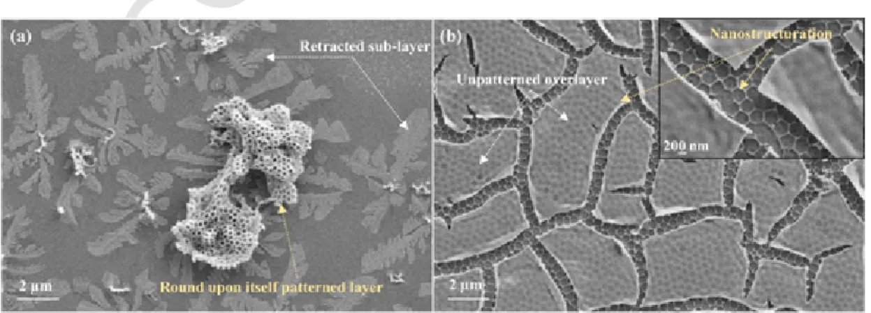
The quality of the nanoparticles (NPs) monolayer is decisive for the achievement of a regular nanostructuring. This was obtained by the LB technique, which is very sensitive to the experimental conditions. The formation of a monolayer of close packed particles was optimized thanks to a thorough study of the influence of several factors such as tempera-ture, compression rate, surface pressure and the amount of nanospheres (see Fig.s S2 and S3 in the SI showing the influence of the concentra-tion of NPs suspensions and that of the withdrawal speed of the substrate respectively). In addition, as aforementioned, the surface of the contin-uous sublayer of YAG:Tb must be smooth and homogeneous in order to obtain a 2D compact and regular packing of nanospheres. Fig. 3 gathers the SEM images of the layers obtained at each step of the patterning.
The YAG:Tb film annealed at 400 °C consists of amorphous film with a smooth and homogeneous surface (Fig. 3a) whereas YAG:Tb film crys-tallized at 1100 °C exhibits cracked, rough and porous surface (Fig. 3b). For these reasons, the deposition of NPs was carried out on the amor-phous coating precursor of YAG:Tb.
Polystyrene (PS) NPs which surface has been modified with func-tional groups of sulphate type are partially of hydrophobic nature. Dur-ing LB deposition, the PS NPs are initially deposited on the surface of
Fig. 3. SEM images of : (a) unpatterned amorphous (annealed at 400 °C) YAG:Tb film; (b) unpatterned crystallized (annealed at 1100 °C) YAG:Tb film; (c) 2D hexagonal close packing NPs
LB film; (d) 2D hexagonal close packing NPs LB film with an overcoating YAG:Tb; (e) 2D patterned surface of YAG:Tb amorphous film and (f) 2D patterned surface of YAG:Tb crystallized film.
UNCORRECTED
PROOF
J.L. Nyalosaso et al. / Chemical Engineering Science xxx (xxxx) 115416 5 the water subphase over which they float. The capillary attraction forces
guided by the concave meniscus, which in turn is induced by gravity be-tween the neighboring colloidal particles, favor compact packing. (Vo-gel et al., 2012) However, the PS NPs, which float on the surface of the water, are so light that they do not sufficiently deform the planar surface of the water so as to cause the phenomenon of compact pack-ing through capillary attraction forces. The compression of the NPs fa-vors the packing of the particles in the hexagonal close packing mode (self-assembly) but maintains a kind of mobility because of the moder-ate polarity of their surface genermoder-ated by the functional sulphmoder-ate groups. The resulting NPs monolayer obtained after evaporation of the water on the substrate and through capillary forces arises therefore as a regular hexagonal packing with some voids between them (Fig. 3c).
The next step of nanostructuring involved the deposition of YAG:Tb precursor sol (overcoating) that uniformly covers the PS NPs as shown in Fig. 3d, while filling the interstices between PS NPs. Removal of PS NPs obtained by calcination at 400 °C results in a relatively ho-mogeneous structure of the luminescent amorphous YAG:Tb coating. The obtained structure is similar to a honeycomb with irregular alveoli (Fig. 3e). This honeycomb structure is consistent with the fact that the PS NPs monolayer was not fully compact. Otherwise, triangular struc-tures not connected to one another would have been obtained. (Zhang and Wang, 2009) Sintering at 1100 °C of the honeycomb structure led to a crystallized YAG:Tb film exhibiting a hexagonal 2D pattern (Fig. 3f). Due to crystallization, the alveoli observed in the amorphous film give way to a more homogeneous hexagonal structure that recalls the hexagonal shape of the PS NPs array. Furthermore, some cracks asso-ciated with the densification of the YAG phase appear on the surface of the crystallized film. The same cracks are found on the unpatterned coating sintered at 1100 °C (Fig. 3b). The sintering is also responsi-ble for the fact that the alveoli (hexagonal cell) are less pronounced (thinner and shallower edges between alveoli) than those of the amor-phous coating. This step has required the optimization of several pa-rameters, in particular the heating rate. For example, a too high heat-ing rate (4 °C/min) caused a too fast subsequent removal of the organic residues, leading to the partial destruction of the structured network. It should be noted that a sufficiently thick sublayer (of the order of 400 nm minimum before sintering at 1100 °C) is necessary to guaran-tee the appearance of a well-organized pattern. Here, as explained in the experimental section, we worked with a sublayer characterized by a thickness around 1 µm. Indeed, during our first attempts of pattern-ing (thickness less than 100 nm), the coatpattern-ing retracted preventpattern-ing struc-turation to occur as shown in Fig. 4a. On the other hand, the amount of YAG:Tb sol used for the overcoating should not be too high, other-wise the PS NPs will be completely covered. In this case, a nanostruc-turing is obtained but largely covered by an unpatterned hollow over-layer, as illustrated in Fig. 4b (hollow spheres let by the removal of PS
spheres may be guessed by darker round areas visible on the overlayer at low magnification).
When deposition parameters are well-defined, the hexagonal net-work obtained in the crystallized coating is preserved over a long range with great fidelity. From SEM images, the periodicity “a” was measured at 490 nm corresponding to the negative imprint left by the PS nanos-pheres of 460 nm.
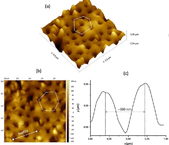
Atomic force Microscopy (AFM) was also used to study nanostruc-tured coatings. Fig. 5 gathers some results obtained from the sample coated with PS NPs whereas Fig. 6 presents AFM images and depth pro-file of the amorphous nanopatterned coating. Other depth propro-files are available in the SI. The AFM images of the PS NPs layer (Fig. 5(a) and (b)) confirm that the PS spheres are homogeneously hexagonally closely packed and the depth profile (Fig. 5 (c)) shows a period of approxi-mately 400 nm between two spheres which is relatively concordant with the SEM images (Fig. 3(c)) and the expected diameter of these commer-cial PS NPs which is of 460 nm. The comparison of different depth pro-files (see Fig. S4(a) in the SI) settles the homogeneity of the NPs depo-sition, which ensured an optimal first step for the following nanostruc-turing.
On the AFM images of the nanopatterned amorphous coating (Fig. 6(a) and (b)), one can observe the presence of hexagonally-organized microwells, as evidenced by SEM images (Fig. 3(e)). Sidewalls seem to be relatively smooth. The depth profile (Fig. 6(c)) shows a period be-tween two edges around 500 nm, which is concordant with the SEM study. The comparison of different depth profiles (see Fig. S4(b)) well establishes the high homogeneity of the nanostructuring.
Furthermore, the mean roughness of the nanostructured amorphous coating was evaluated around 50 nm (RMS) thanks to Gwyddion soft-ware whereas the unpatterned one was characterized by a RMS around 0.5 nm. (Potdevin et al., 2009) This should have consequences on the optical properties of these samples since an increased RMS generally en-tails a decrease in the waveguiding properties of the coating. (Kim et al., 2016) The RMS slightly decreases for the crystallized nanostruc-tured sample (RMS around 40 nm) which is probably due to the phe-nomenon of densification accompanying the crystallization. Sidewalls and microwells are then less sharp and deep respectively as schematized in the Fig. S5. In this case, the differences between the rugosity of the unpatterned crystallized coating and that of the patterned one are less pronounced than between the two amorphous samples.
3.3. Luminescence properties and characterization of the light extraction by the surface patterning
Fig. 7 shows the room-temperature excitation spectra of unpat-terned amorphous (Fig. 7(a)) and crystallized (Fig. 7b) YAG:Tb dip-coated layers in the VUV and in a part of the UV wavelength
ranges. It
UNCORRECTED
PROOF
Fig. 5. (a) 3D AFM image, (b) 2D AFM image and (c) depth profile of 2D hexagonal close packing PS NPs obtained by the LB method on the sub-layer of amorphous YAG:Tb precursor.
is assumed that patterned samples are characterized by similar excita-tion profiles.
The crystallized layer (Fig. 7b) presents an excitation spectrum close to those obtained for YAG:Tb powders (Potdevin et al., 2007) with several broad bands. The main one is located around 172 nm and cor-responds to the band absorption of the host lattice (Mayolet et al., 1995; Park et al., 2000) since the band gap energy of YAG is ap-proximately 7.0 eV. This band originates from a partial energy transfer between the host and the luminescent centers. Besides, three other ab-sorption bands located at 203, 227 nm and 271 nm are observed. Tb3+
ions exhibit a 4f8configuration for which the ground state is7F6. The
4f75d1first excited configuration presents two spin states: the high spin 9DJ(or9E) and the low-spin7DJ(or7E) (J = 0…5). The bands at 227
and 271 nm can be attributed to the spin-allowed7F6→7D4and7F6→7D5
transitions respectively. The weak signal located at 203 nm is also re-lated to 4f → 5d Tb3+transitions and more particularly to the
spin-for-bidden7F6→9D3transition (Dorenbos, 2003), which explains why this
signal is so weak. One can also observe the onset of a signal around 320 nm, already evidenced in sol-gel derived YAG:Tb powders (Pot-devin et al., 2010b) and which can be ascribed to another spin-for-bidden transition,7F6→9D2(Dorenbos, 2003). This excitation profile,
characteristic of YAG:Tb3+phase, confirms the negligible effect of the
presence of a weak amount of YAM phase evidenced by XRD (Fig. 2). Concerning the amorphous coating (Fig. 7a), we can notice that the main absorption band corresponding to the host excitation has van-ished, which is consistent with the amorphous character of the sam-ple. Two very broad excitation bands can be observed around 191 and 233 nm. Based on previous studies led on amorphous powders, (Pot-devin et al., 2010a) we can assume they are related to inter-shell
4f → 5d Tb3+transitions. The spectral distribution of these transitions is
strongly influenced by the strength and symmetry of crystal-field under-gone by the active ions. (Blasse and Grabmaier, 1994) In the aspect of crystal-field theory, amorphous phases exhibit lower symmetry and weaker crystal-field strength induced by the neighboring ions if com-pared with crystallized ones. These differences in the Tb3+local
envi-ronment logically entail a blue-shift of excitation bands of the amor-phous coating (Fig. 7a) compared to those obtained for the crystallized sample (Fig. 7b).
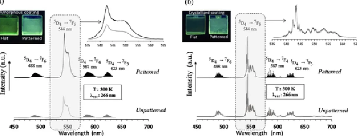
Even if it is not the best excitation wavelength for the amorphous samples, we recorded emission spectra under a 266 nm excitation (im-posed by the experimental set-up). Fig. 8 gathers emission spectra of the nanostructured and unstructured films for both forms of YAG:Tb, amor-phous and crystallized. These emission spectra exhibit profiles charac-teristic of both amorphous and crystallized YAG:Tb powders with a main emission band peaking in the green region. (Potdevin et al., 2010a). It is important to emphasize that crystallization significantly enhanced emission intensity, as already reported in (Potdevin et al., 2009) and as shown in Fig. S6 gathering emission spectra of amorphous and crys-tallized unpatterned samples. In Fig. 8, scales have been chosen to be as adapted as possible to the data and are not comparable between Fig. 8a and b.
Photographs corresponding to the samples are also presented in Fig. 8. These pictures have been taken using a camera that automatically ad-justed recording conditions to have the best sharpness. As a result, pho-tographs are not comparable. However, they evidence the bright green luminescence of all samples and the diffusive effect brought by the pat-terning.
The spectra of the amorphous coatings show broad emission bands linked to the Tb3+ions multisite character (Fig. 8a) while the Stark
UNCORRECTED
PROOF
J.L. Nyalosaso et al. / Chemical Engineering Science xxx (xxxx) 115416 7
Fig. 6. (a) 3D AFM image, (b) 2D AFM image and (c) depth profile of the amorphous nanopatterned coating after removal of PS NPs.
Fig. 7. Excitation spectra of (a) amorphous and (b) crystallized (heated at 1100 °C)
unpat-terned coatings.
components are well distinguished on the spectra of the crystallized coatings (Fig. 8b).
The observed bands can be ascribed to the electronic transitions from the5D4first excited level of the Tb3+ions to the 7FJmanifolds
(J = 6…0) of the ground state. The most intense band (λem= 544 nm)
corresponds to the transition between the5D4 and 7F5 levels of the
Tb3+ions. The insets of the Fig. 8 represent this main transition,
high-lighting the influence of the nanopatterning on the emission intensity,
deduced from the integrated area of this band in all cases. The emis-sion intensity corresponding to the5D4→7F5transition is more
impor-tant for the patterned films. This enhancement reaches 26% in the case of crystallized films and 131% in the case of amorphous films, while the amount of phosphor remains similar when comparing unpatterned and patterned samples. This gain can also be defined by the so-called “en-hanced extraction factor” (EEF) which corresponds to the ratio between the intensities of nanostructured films and unstructured ones, phosphors amounts being equal in both samples. The EEF is 1.1 in the case of crys-tallized films and 2.3 in the case of amorphous samples.
This means that nanostructuring could be used to increase the extrac-tion of the light produced by luminescence previously entrapped in the substrate. Furthermore, the deeper the nanostructuring is (the higher the RMS is), the more efficient the light extraction will be. (Devys et al., 2014) Indeed, the nanopatterning of the amorphous coatings is more marked than that of the crystallized coatings (see Fig. 3e and f and RMS measurements by AFM), as illustrated by the schemes gathered in Fig. S5. This phenomenon has already been observed by Kim et al. 2016 on roughened surfaces used for the deposition of a silicate phosphor for LEDs applications. It can be ascribed to the growth in opportunities for photons to find broader escape angles with increasing surface roughness. (Khan et al., 2019; Kim et al., 2016)
Unstructured amorphous samples are those in which waveguide phe-nomena are the most present, RMS the weakest and therefore those for which the extraction efficiency is worst. They are transparent under daylight and very smooth, which promoted the waveguiding phenom-ena. When they are patterned, they become more diffusing, and their RMS significantly increase, which surely entails a decrease in the num-ber of guided modes within the layer. (Gorsky et al., 2018; Kim et al., 2016) As mentioned before, the light diffusing effect on the pat
UNCORRECTED
PROOF
Fig. 8. Room-temperature emission spectra (λexc= 266 nm) of Tb3+for patterned (black) and unpatterned (grey) films annealed at a) 400 °C and b) 1100 °C. Insets are the superposition
of the patterned (black) and unpatterned (grey) films spectra (λem: 535–565 nm) in order to highlight the difference in intensity and integrated area.
terned coatings is clearly demonstrated in the photos of the coated sub-strates in Fig. 8.
3.4. Qualitative and quantitative angle-resolved luminescence measurements
In order to study the effect of nanostructuring on the directional-ity of the PL, angular emission measurements were carried out on both unstructured and nanostructured crystallized YAG:Tb films. The lumi-nescence diagrams I (color scale) given in Fig. 9a-1 and b-1 repre-sent the emission spectra for the main emission band located between 540 and 560 nm as a function of the detection angle θ. The diagrams were recorded from θ = −30° to θ = +30° and between 540 nm and 560 nm (0° corresponding to a light perpendicular to the layer). The highest the color temperature is, the strongest the emission intensity is. As aforementioned, emission profiles are characteristic of Tb3+ions in
crystalline matrices, with an intense emission band peaking at 544 nm
corresponding to the5D4→7F5transition. The luminescence diagrams
are different depending on whether the film is patterned or not. For the nanostructured surface, the false color intensity diagram shows that the intensity of the spectrum is maximum at θ = 0°. This re-sult demonstrates that the emission intensity of Tb3+depends on the
detection angle θ when the surface is nanostructured in a hexagonal lat-tice. The light extraction is therefore directional in this case.
The EEF was calculated by integrating the emission bands in the region of 535–550 nm over θ =+30°, θ = 0° and θ = −30°, and by making the ratio of the calculated areas. Fig. 9a-2 and b-2 represent the superposition of these emission bands for both the nanostructured and unstructured films. In the case of the unstructured film, no dif-ference was observed between the emission bands on the three detec-tion angles. The emission intensity was found isotropic indicating that no direction was favored. On the other hand, in the case of the struc-tured film, the emission distribution was preferably centered on θ = 0°.
Fig. 9. Luminescence maps corresponding to the emission spectra detected at different angle positions for : (a-1) unpatterned and (a-2) patterned films of crystallized YAG:Tb. The colour
code represents the emission intensity. (a-2) and (b-2) represent the emission spectra recorded at angles −30°, 0°and + 30° for the unpatterned and patterned films of crystallized YAG:Tb, respectively.
UNCORRECTED
PROOF
J.L. Nyalosaso et al. / Chemical Engineering Science xxx (xxxx) 115416 9 Moreover, we found an EEF of 1.5 between the emission at θ = 0° and
θ = ± 30°. Due to nanostructuring, 1.5 times more light intensity was extracted at θ = 0° (forward emission). By analogy with the study of the influence of the depth of photonic crystals patterns on the light ex-traction reported by Devys et al. 2014), this phenomenon can be asso-ciated with a coupling between the waveguide and the hexagonal com-pact (shape factor) network in a given direction, in this case at θ = 0°.
In conclusion, with similar amounts of phosphor, the structuration allows a significant increase in the emission intensity and can act on the angular dependence of this intensity, by increasing the extraction of light perpendicularly to the surface. It should be pointed out that, through structuration, it will therefore be possible to control the light output angle in order to have a stable light quality over angular ranges from (−30° / +30°) to (−60° / +60°) depending on the targeted appli-cation, instead of the 4π steradians obtained without structuration.
Finally, these results are a proof of concept that can be applied to all matrices synthesizable by sol-gel, in particular the YAG:Ce used in the more conventional solid state lighting devices. As indicated in the intro-duction, the YAG:Tb matrix was used in this study because it is charac-terized by a bright green luminescence readily detectable with the naked eyes upon standard UV lamps and during angular resolved PL. Based on several reports and on first simulations led on YAG:Ce, light extraction enhancement can be further improved by optimizing the geometric pa-rameters of the patterned network as well as by working with textured substrate (resulting in texture on both sides of the AL). (Gorsky et al., 2018; Kim et al., 2016; Mao and Karlicek, 2013)
4. Conclusion
Patterned films of YAG:Tb (20%) were prepared for the first time on quartz slides using an innovative and versatile approach combin-ing sol-gel chemistry with colloidal lithography carried out by the LB technique. These films were compared with their unpatterned equiva-lents in their amorphous and crystallized states for the purpose of study-ing forward light extraction. It was demonstrated in this study that nanopatterning YAG:Tb films in a hexagonal close-packing network with a 460 nm grating has an influence on the light path by reducing the losses mainly linked to internal reflections. Photoluminescence spec-troscopy was used to determine the gain in forward photoluminescence, due to nanostructuring, which was found to be 26% in the case of crys-tallized films and 131% in amorphous films. This study was first devoted to YAG:Tb matrix with the purpose of establishing a proof of concept before extending the structuring process to other matrices such as the YAG:Ce, used in current LED lighting systems. Because this structuration process can be applied to many different sol-gel-derived phosphors, it represents a very promising means to create patterned luminescent coat-ings, for which patterning parameters could be tuned (by changing the size of PS beads for example) to match the targeted application. Indeed, as shown by these first results, by engineering the shape of the structure (especially the height and the sharpness of the walls of the microwells) we can access to a controlled roughness that should entail a significant enhancement of luminescence of these coatings, which is very interest-ing in the aim of combination with LEDs. Further works should be dedi-cated to the patterning of YAG:Ce matrix and the study of the influence of the patterning network parameters on the optical properties of struc-tured coatings, based on both simulations and experiences. Preliminary experiments involving the YAG:Ce matrix are currently under investiga-tion and first simulainvestiga-tions concerning these patterned coatings have fore-seen significant changes on emission spectral distribution.
5. Funding sources
This work was supported by the Région Auvergne-Rhône-Alpes (Op-tilum project); European Community for its financial support during
the access to VUV spectroscopy facilities DESY (Contract RII3-CT-2004-506008).
CRediT authorship contribution statement
Jeff Nyalosaso: Investigation, Writing - original draft. Audrey Pot-devin: Supervision, Writing - original draft, Writing - review & edit-ing, Visualization, Funding acquisition. François Réveret: Investiga-tion. Pierre Disseix: Supervision. Rachid Mahiou: InvestigaInvestiga-tion. Geneviève Chadeyron: Conceptualization, Funding acquisition. Declaration of Competing Interest
The authors declared that there is no conflict of interest. Acknowledgements
The authors thank the Région Auvergne-Rhône-Alpes for its finan-cial support (Optilum project), Christelle Blavignac, Claire Szczepaniak, Lorraine Novais Gameiro (Centre Imagerie Cellulaire Santé – Univer-sité Clermont Auvergne, France) and Anne-Marie Gélinaud (2Matech, Aubière, France) for their technical support and expertise for SEM ob-servations as well as David Bourgogne (ICCF, Clermont-Ferrand) for his advices during AFM study. The authors also acknowledge DESY and the European Community respectively for the access of VUV spectroscopy facilities and the financial support (Contract RII3-CT-2004-506008). Appendix A. Supplementary material
Supplementary data to this article can be found online athttps://doi. org/10.1016/j.ces.2019.115416.
References
Ai, B., Möhwald, H., Wang, D., Zhang, G., 2017. Advanced colloidal lithography beyond surface patterning. Adv. Mater. Interfaces 4, 1600271. doi:10.1002/admi.201600271. Akaltun, Y., Yıldırım, M.A., Ateş, A., Yıldırım, M., 2011. The relationship between refrac-tive index-energy gap and the film thickness effect on the characteristic parameters of CdSe thin films. Opt. Commun. 284, 2307–2311. doi:10.1016/j.optcom.2010.12.094. Bardosova, M., Pemble, M.E., Povey, I.M., Tredgold, R.H., 2010. The langmuir-blodgett approach to making colloidal photonic crystals from silica spheres. Adv. Mater. 22, 3104–3124. doi:10.1002/adma.200903708.
Blasse, G., Grabmaier, B.C., 1994. Luminescent Materials. Springer-Verlag, Berlin. Brinker, C.J., Scherer, G.W., 2013. Sol-Gel Science: The Physics and Chemistry of Sol-Gel.
Processing. Elsevier Science.
Cho, J., Park, S.-J., Ahn, J., Lee, H., 2014. Nanopatterned yttrium aluminum garnet phos-phor incorporated film for high-brightness GaN-based white light emitting diodes. Thin Solid Films 570, 326–329. doi:10.1016/j.tsf.2014.03.065.
Cho, J.Y., Ko, K.-Y., Do, Y.R., 2007. Optical properties of sol–gel derived Y2O3:Eu3+
thin-film phosphors for display applications. Thin Solid Films 515, 3373–3379. doi:10.1016/j.tsf.2006.09.029.
Colson, P., Cloots, R., Henrist, C., 2011. Experimental design applied to spin coating of 2D colloidal crystal masks: a relevant method? Langmuir 27, 12800–12806. doi:10.1021/ la202284a.
Colson, P., Henrist, C., Cloots, R., 2013. Nanosphere lithography: a powerful method for the controlled manufacturing of nanomaterials. J. Nanomater. 2013, 21. doi:10.1155/ 2013/948510.
Devys, L., Dantelle, G., Revaux, A., Kubytskyi, V., Paget, D., Benisty, H., Gacoin, T., 2014. Extraction length determination in patterned luminescent sol-gel films. Adv. Opt. Mater. 2, 81–87. doi:10.1002/adom.201300304.
Ding, P., Shao, L., Wang, J., Li, Y., Zeng, F., Liang, E., 2017. Enhanced light extraction with silicon nanoantenna arrays for white light LED applications. Opt. Quant. Electron. 49, 194. doi:10.1007/s11082-017-1035-2.
Do, Y.R., Kim, Y.-C., Shin, N., Sohn, K.-S., 2005. Enhanced light extraction efficiency in pulse laser deposited Gd2O3: Eu3+thin-film phosphors on 2-D PCLs. Electrochem.
Solid-State Lett. 8, H43–H45. doi:10.1149/1.1887191.
Dorenbos, P., 2003. Exchange and crystal field effects on the 4f(n-1)5d levels of Tb3+. J.
Phys.: Condens. Matter 15, 6249–6268. doi:10.1088/0953-8984/15/36/313. Fang, C.-Y., Liu, Y.-L., Lee, Y.-C., Chen, H.-L., Wan, D.-H., Yu, C.-C., 2013. Nanoparticle
stacks with graded refractive indices enhance the omnidirectional light harvesting of solar cells and the light extraction of light-emitting diodes. Adv. Funct. Mater. 23, 1412–1421. doi:10.1002/adfm.201201949.
UNCORRECTED
PROOF
Ge, Z., Piquette, A., Mishra, K.C., Klotzkin, D., 2015. Enhanced forward emission of YAG:Ce3+phosphor with polystyrene nanosphere coating. Appl. Opt. 54, 6025–6028.
doi:10.1364/AO.54.006025.
Geng, C., Wei, T., Wang, X., Shen, D., Hao, Z., Yan, Q., 2014. Enhancement of light out-put power from leds based on monolayer colloidal crystal. Small 10, 1668–1686. doi:10.1002/smll.201303599.
Gorsky, S., Zhang, R., Gok, A., Wang, R., Kebede, K., Lenef, A., Raukas, M., Negro, L.D., 2018. Directional light emission enhancement from LED-phosphor converters using dielectric Vogel spiral arrays. APL Photonics 3, 126103. doi:10.1063/1.5052637. Khan, M.A., Bian, P., Qu, J., Chen, H., Liu, H., Foley, M., Yao, Y., Ringer, S.P., Zheng, R.,
2019. Non-destructive analysis on nano-textured surface of the vertical LED for light enhancement. Ultramicroscopy 196, 1–9. doi:10.1016/j.ultramic.2018.09.003. Khanna, V.K., 2014. Fundamentals of Solid-State Lighting: LEDs, OLEDs, and Their
Appli-cations in Illumination and Displays. CRC Press.
Kim, J.S., Eswaran, S.K., Kwon, O.H., Han, S.J., Lee, J.H., Cho, Y.S., 2016. Enhanced lu-minescence characteristics of remote yellow silicate phosphors printed on nanoscale surface-roughened glass substrates for white light-emitting diodes. Adv. Opt. Mater. 4, 1081–1087. doi:10.1002/adom.201500734.
Ko, K.Y., Lee, K.N., Lee, Y.K., Do, Y.R., 2008. Enhanced light extraction from SrGa2S4:
Eu2+film phosphors coated with various sizes of polystyrene nanosphere monolayers.
J. Phys. Chem. C 112, 7594–7598.
Kumar, P., Son, S.Y., Singh, R., Balasundaram, K., Lee, J., Singh, R., 2011. Analytical treat-ment of light extraction from textured surfaces using classical ray optics. Opt. Com-mun. 284, 4874–4878. doi:10.1016/j.optcom.2011.06.062.
Lee, Y.K., Oh, J.R., Do, Y.R., 2007. Enhanced extraction efficiency of Y2O3: Eu3+thin-film
phosphors coated with hexagonally close-packed polystyrene nanosphere monolayers. Appl. Phys. Lett. 91, 041907. doi:10.1063/1.2763974.
Lenef, A., Piquette, A., Kelso, J., 2018. Thermodynamics of light extraction from lumi-nescent materials. ECS J. Solid State Sci. Technol. 7, R3211–R3226. doi:10.1149/ 2.0271801jss.
Liang, X., Dong, R., Ho, J.C., 2019. Self-assembly of colloidal spheres toward fabrication of hierarchical and periodic nanostructures for technological applications. Adv. Mater. Technol. 4, 1800541. doi:10.1002/admt.201800541.
Mao, A., Karlicek, R.F., 2013. Surface patterning of nonscattering phosphors for light ex-traction. Opt. Lett. 38, 2796–2799. doi:10.1364/ol.38.002796.
Mayolet, A., Zhang, W., Simoni, E., Krupa, J.C., Martin, P., 1995. Investigation in the VUV range of the excitation efficiency of the Tb3+ion luminescence in Y3(Alx, Gay)5O12
host lattices. Opt. Mater. 4, 757–769. doi:10.1016/0925-3467(95)00024-0. McKittrick, J., Shea-Rohwer, L.E., 2014. Review: down conversion materials for solid-state
lighting. J. Am. Ceram. Soc. 97, 1327–1352. doi:10.1111/jace.12943.
Mergel, D., Buschendorf, D., Eggert, S., Grammes, R., Samset, B., 2000. Density and re-fractive index of TiO2films prepared by reactive evaporation. Thin Solid Films 371,
218–224. doi:10.1016/S0040-6090(00)01015-4.
Narendran, N., Gu, Y., Freyssinier-Nova, J.P., Zhu, Y., 2005. Extracting phosphor-scat-tered photons to improve white LED efficiency. Phys. Status Solidi (a) 202, R60–R62. doi:10.1002/pssa.200510015.
Park, B.K., Park, H.K., Oh, J.H., Oh, J.R., Do, Y.R., 2012. Selecting morphology of Y3Al5O12: Ce3+phosphors for minimizing scattering loss in the pc-LED package. J.
Electrochem. Soc. 159, J96–J106. doi:10.1149/2.031204jes.
Park, C.-H., Park, S.-J., Yu, B.-Y., Bae, H.-S., Kim, C.-H., Pyun, C.-H., Guang-Yan, H., 2000. VUV excitation of Y3Al5O12: Tb phosphor prepared by a sol-gel process. J. Mater. Sci. Lett. 19, 335–338. doi:10.1023/A:1006727116993.
Piquette, A., Bergbauer, W., Galler, B., Mishra, K.C., 2016. On choosing phosphors for near-UV and blue LEDs for white light. ECS J. Solid State Sci. Technol. 5, R3146–R3159. doi:10.1149/2.0191601jss.
Potdevin, A., Briois, V., Caperaa, N., Santilli, C.V., Chadeyron, G., Mahiou, R., 2016. A thorough spectroscopic study of luminescent precursor solution of Y3Al5O12:Tb3+:
in-fluence of acetylacetone. RSC Adv. 6, 41962–41971. doi:10.1039/c6ra06444b. Potdevin, A., Chadeyron, G., Boyer, D., Mahiou, R., 2006. Production and shaping of
high performance phosphors by using the sol-gel process: yttrium aluminum gar-net (Y3Al5O12). J. Non-Cryst. Solids 352, 2510–2514. doi:10.1016/
j.jnoncrysol.2006.03.046.
Potdevin, A., Chadeyron, G., Boyer, D., Mahiou, R., 2006. Sol-gel elaboration and char-acterization of YAG: Tb3+ powdered phosphors. J. Mater. Sci. 41, 2201–2209.
doi:10.1007/s10853-006-7182-7.
Potdevin, A., Chadeyron, G., Boyer, D., Mahiou, R., 2007. Optical properties upon vac-uum ultraviolet excitation of sol-gel based Y3Al5O12:Tb3+, Ce3+ powders. J. Appl. Phys. 102, 073536–073536, https://doi.org/10.1063/1.2784998.
Potdevin, A., Chadeyron, G., Briois, V., Leroux, F., Mahiou, R., 2010. Modifications in-volved by acetylacetone in properties of sol-gel derived Y3Al5O12:Tb3+- II: optical
features. Dalton Trans. 39, 8718–8724. doi:10.1039/C0DT00090F.
Potdevin, A., Chadeyron, G., Briois, V., Mahiou, R., 2011. Structural, morphological and scintillation properties of Ce3+-doped Y3Al5O12powders and films elaborated
by the sol-gel process. Mater. Chem. Phys. 130, 500–506. doi:10.1016/ j.matchemphys.2011.07.019.
Potdevin, A., Chadeyron, G., Mahiou, R., 2010. Tb3+-doped yttrium garnets:
promis-ing tunable green phosphors for solid-state lightpromis-ing. Chem. Phys. Lett. 490, 50–53. doi:10.1016/j.cplett.2010.03.003.
Potdevin, A., Lechevallier, S., Chadeyron, G., Caperaa, N., Boyer, D., Mahiou, R., 2009. Waveguiding terbium-doped yttrium aluminum garnet coatings based on the sol-gel process. Thin Solid Films 517, 4610–4614. doi:10.1016/j.tsf.2009.02.087. Reculusa, S., Ravaine, S., 2003. Synthesis of colloidal crystals of controllable thickness
through the Langmuir− Blodgett technique. Chem. Mater. 15, 598–605. doi:10.1021/ cm021242w.
Revaux, A., Dantelle, G., Decanini, D., Guillemot, F., Haghiri-Gosnet, A.-M., Weisbuch, C., Boilot, J.-P., Gacoin, T., Benisty, H., 2011. Photonic crystal patterning of lumi-nescent sol–gel films for light extraction. Nanotechnology 22, 365701. doi:10.1088/ 0957-4484/22/36/365701.
Schnitzer, I., Yablonovitch, E., Caneau, C., Gmitter, T.J., Scherer, A., 1993. 30% external quantum efficiency from surface textured, thin-film light-emitting diodes. Appl. Phys. Lett. 63, 2174–2176. doi:10.1063/1.110575.
Shionoya, S., 1998. Phosphor Handbook. CRC Press, Boca Raton.
Sohn, K.-S., Shin, N., Kim, Y.-C., Do, Y.R., 2004. Effect of corrugated substrates on light ex-traction efficiency and the mechanism of growth in pulsed laser deposited Y2O3:Eu3+
thin-film phosphors. Appl. Phys. Lett. 85, 55–57. doi:10.1063/1.1766392. Sun, H., Piquette, A., Raukas, M., Moustakas, T.D., 2016. Enhancement of yellow light
extraction efficiency of Y3Al5O12: Ce3+ceramic converters using a 2-D TiO2
hexag-onal-lattice nanocylinder photonic crystal layer. IEEE Photonics J. 8, 1–10. doi:10.1109/jphot.2016.2527019.
Szabó, Z., Volk, J., Fülöp, E., Deák, A., Bársony, I., 2013. Regular ZnO nanopillar ar-rays by nanosphere photolithography. Photon. Nanostruct.-Fundamen. Appl. 11, 1–7, http://dx.doi.org/10.1016/j.photonics.2012.06.009.
Tian, Y., Chen, M., Zhang, J., Tong, Y.-L., Wang, C.-F., Wiederrecht, G.P., Chen, S., 2018. Highly enhanced luminescence performance of LEDs via controllable layer-struc-tured 3D photonic crystals and photonic crystal beads. Small Methods 2, 1800104. doi:10.1002/smtd.201800104.
Ulman, A., 2013. An Introduction to Ultrathin Organic Films: From Langmuir-Blodgett to Self–Assembly. Academic press.
Vogel, N., Retsch, M., Fustin, C.-A., del Campo, A., Jonas, U., 2015. Advances in colloidal assembly: the design of structure and hierarchy in two and three dimensions. Chem. Rev. 115, 6265–6311. doi:10.1021/cr400081d.
Vogel, N., Weiss, C.K., Landfester, K., 2012. From soft to hard: the generation of functional and complex colloidal monolayers for nanolithography. Soft Matter 8, 4044–4061. doi:10.1039/c1sm06650a.
Wang, S., Li, Y., Feng, L., Zhang, L., Zhang, Y., Su, X., Ding, W., Yun, F., 2016. Laser pat-terning of Y3Al5O12:Ce3+ceramic phosphor platelets for enhanced forward light
ex-traction and angular color uniformity of white LEDs. Opt. Express 24, 17522–17531. doi:10.1364/OE.24.017522.
Wang, S., Zhou, T., Li, D., Zhong, Z., 2016. Evolution and engineering of precisely con-trolled ge nanostructures on scalable array of ordered Si nano-pillars. Sci. Rep. 6, 28872. doi:10.1038/srep28872.
Yang, X., Dev, K., Wang, J., Mutlugun, E., Dang, C., Zhao, Y., Liu, S., Tang, Y., Tan, S.T., Sun, X.W., Demir, H.V., 2014. Light extraction efficiency enhancement of colloidal quantum dot light-emitting diodes using large-scale nanopillar arrays. Adv. Funct. Mater. 24, 5977–5984. doi:10.1002/adfm.201400190.
Youn, W., Lee, J., Xu, M., Singh, R., So, F., 2015. Corrugated sapphire substrates for or-ganic light-emitting diode light extraction. ACS Appl. Mater. Interfaces 7, 8974–8978. doi:10.1021/acsami.5b01533.
Zhang, G., Wang, D., 2009. Colloidal lithography—the art of nanochemical patterning. Chem. Asian J. 4, 236–245. doi:10.1002/asia.200800298.
Zhmakin, A.I., 2011. Enhancement of light extraction from light emitting diodes. Phys. Rep. 498, 189–241. doi:10.1016/j.physrep.2010.11.001.
Zimmerer, G., 2007. SUPERLUMI: A unique setup for luminescence spectroscopy with syn-chrotron radiation. Radiat. Meas. 42, 859–864. doi:10.1016/j.radmeas.2007.02.050.