Circuit Designs for the MAP Chip
by
Andrew R. Chen
Submitted to the Department of Electrical Engineering and Computer Science
in partial fulfillment of the requirements for the degree of
Master of Engineering in Electrical Engineering and Computer Science
at the
MASSACHUSETTS INSTITUTE OF TECHNOLOGY
May 1997
@ Andrew R. Chen, MCMXCVII. All rights reserved.
The author hereby grants to MIT permission to reproduce and distribute publicly
paper and electronic copies of this thesis document in whole or in part, and to grant
others the right to do so.
A uthor...
... ...
Department of Electrical Engineering and Computer Science
May 1, 1997
Certified by . .. ..
..
.
William J. Dally
Professor
Thesis Supervisor
Accepted by... .
.
......
S...m it h...
...
A. C.
Smith
Andrew R. Chen
Submitted to the Department of Electrical Engineering and Computer Science on May 1, 1997, in partial fulfillment of the
requirements for the degree of
Master of Engineering in Electrical Engineering and Computer Science
Abstract
This thesis describes some of the many circuit-level designs included in the M-Machine Multi-ALU Processor (MAP Chip). Standard cells have been created or modified to reduce the area and propagation delay of synthesized logic. The global clock distribution system has been designed at the circuit level and preliminary simulations performed. The Local Translation Lookaside Buffer (LTLB), consisting of SRAM arrays and standard cell logic, has been implemented using components similar to those in other MAP Chip memory arrays.
Thesis Supervisor: William J. Dally Title: Professor
Acknowledgments
The M-Machine project has been an extremely challenging and instructive experience, and the most valuable professional experience I have encountered thus far. Thanks to Bill Dally for bringing me in to the group and providing a vast amount of knowledge and guidance. Thanks to all the M-Machiners for making this a great project.
I owe very deep thanks to my family for supporting me over the years. And thanks to my friends who have become my family when I'm away from home.
1 Introduction 9 1.1 Overview ... ... 9 1.1.1 The M -M achine ... ... 9 1.1.2 O utline . . . . . . ... 10 2 Standard Cells 12 2.1 Introduction .. . . . .. . .. . . . ... . . 12 2.2 Latches . . . ... . . 12 2.2.1 Introduction ... ... 12 2.2.2 Circuit Designs ... ... ... 13 2.2.3 Implementation ... 15 2.2.4 Usage ... ... 17 2.2.5 Function . .. . . . .. . . . .. . . . .. . . .. .. . 19 2.2.6 Evaluation .. ... ... .. ... ... ... . .. ... .. .... . 21 2.3 Register Cell . . . ... . . 25 2.3.1 Background ... 25 2.3.2 D esign . . . ... . . 26 2.3.3 Implementation ... 27 2.3.4 Evaluation .. .. . .. . .. . .. ... ... ... ... .. ... 28 2.3.5 Arrays: GTLB ... 31
2.3.6 Low Threshold Inverter ... 32
2.3.7 Sum m ary . .. ... ... .. ... ... ... . .. . .. . . ... 33
2.4 Logic Cells .. . . . .. . . . .... . . 34
3.1 Introduction .
3.2 Design ... .
3.2.1 Overview . . . .
3.2.2 W ires and W ire Models ...
3.2.3 Differential Buffers ...
3.2.4 Pulse Generators ... ...
3.3 Sources of Clock Skew ...
3.4 Evaluation . . . .. . . . .. 3.4.1 Differential Buffers ... 3.4.2 Pulse Generators ... 3.5 Power Dissipation ... ... ... ... .... 3.6 Layout Issues . . . . 3.6.1 Differential Buffers ... 3.6.2 Interconnect . . . . 3.6.3 Electrom igration ... ... .. 4 Design of the LTLB 4.1 Introduction . . . .... 4.2 Function . . . . . 4.3 Implementation ... ... ... 4.3.1 Overview .. . . . .. . . . ... 4.3.2 D atapath . . . . 4.3.3 Cell Descriptions . . . .. 4.3.4 LTLB_ARRAY_HALF . . . . 4.4 Cell Reuse . . . . . 4.5 Layout . . . .. ... 4.6 Evaluation ... ... 4.7 Shrink . . . . 5 Conclusion 5.1 Sum m ary . . . . 5.2 And Finally... . . . . 37
A.2 Clock Distribution System ... ... 82
List of Figures
1-1 M-Machine Architecture ... 10
1-2 MAP Chip Architecture ... 11
2-1 MAP Chip positive latch. ... 13
2-2 Scannable registers, illustrating normal and scan operation. . ... 13
2-3 High-level design of the MAP Chip Scannable Paths. . ... 14
2-4 Block diagrams of PDFFSCAN and NLTCHSCAN . ... 15
2-5 PMOS with keeper vs. complementary passgate . . . . 16
2-6 Two methods for generating a gated clock. . ... 17
2-7 Timing diagram for PDFFSCAN ... 18
2-8 Timing diagram for NLTCHSCAN ... 18
2-9 Typical waveforms for noise testing ... 19
2-10 Six-transistor SRAM Cell ... 25
2-11 Arrays of the register cell used in queues. . ... 26
2-12 The CAM cell and its arrangment in the GTLB. . ... . . . . 27
2-13 Model for capacitive load of arrays ... 30
2-14 Setup time for register cell ... 31
2-15 Read time for register cell ... 31
2-16 Schematic for INV_IR... ... 32
2-17 Transfer curve for INV_IR at TTL conditions. . ... . 33
2-18 weak NAND, AND with buffer, and proposed NAND_2... 34
2-19 Circuit to evaluate logic gate propagation delay. ... . . . . . 35
3-1 Global Clock Distribution. ... 38
3-5 3-6 4-1 4-2 4-3 4-4 4-5 4-6 4-7 4-8 4-9
Layout with dim( Writing of bit ce Precharging of b
ensions and positions of major components..
11, T TL .. . . . .
itlines, TTL . . . . .
Noise Test Waveforms for DIDO ... Noise Test Waveforms for DISOPG . ...
LTLB SRAM Array Block Diagram . . . . .
LTLBRAM Block Diagram. . ...
Concept for Output and Read-Modify- Write selector Numbering of sub-arrays and their control signals. Organization of standard-cells and custom cells. ...
Data organization within LTLB_ARRAYADDR. ..
Data organization within LTLBARRA YSTATUS. .
Timing chain signals, TTL conditions. ... .
Decode clock (DC) signal timing, TTL conditions.
4-10 LTLB Layout..
4-11 4-12 4-13
Chapter 1
Introduction
1.1
Overview
The M-Machine is an experimental multicomputer being developed at the Massachusetts Institute of Technology. It will be used to investigate methods for parallelism, efficient and innovative uses of high-performance integrated circuit technology, and to support ex-perimental parallel software. It is organized as a three dimensional mesh of nodes, each
containing a Multi-ALU Processor (MAP) and conventional DRAM.
This thesis describes some of the many circuit-level design efforts that contibute to the MAP Chip, including standard cells, clock distribution, and implementation of the LTLB memory array.
1.1.1 The M-Machine
One goal of the M-Machine architecture is to efficiently utilize DRAM, which typically occupies the vast majority of silicon area in the system. In contrast to conventional designs where a large amount of memory is dedicated to a single processor, each M-Machine node contains 8MB of DRAM[6].
The MAP Chip includes three execution clusters, network and memory subsystems. Execution clusters on the MAP Chip are analogous to RISC microprocessor cores, each being a a 64-bit three-issue, fully pipelined microprocessor. Memory requests are issued over the M-Switch, and the C-Switch carries inter-cluster communications and return data from the memory system. The MAP Chip has a target cycle time of 10 nanoseconds, corresponding to 100MHz.
.0 YAdir Z-dir
Figure 1-1: M-Machine Architecture
1.1.2
Outline
Modules in the MAP Chip are divided into control and datapath sections. Generally, data-paths are time-critical and include full-custom circuit design. Control logic and less-critical circuits will be synthesized from standard cells. A set of latches suitable for the M-Machine diagnostic methodology has been developed [3]. A static latch cell (register cell) similar to the classic six-transistor SRAM cell is used in small arrays including network queues. Large-sized cells with stronger output drive have been designed to reduce propagation delays, and the need for buffering, in synthesized logic.
Clock distribution is a challenging design task for the MAP Chip. Special attention to signal distribution is necessary because of the its large die size and high clock speed. Differential reference signals are carried by a tree structure with three levels of buffering. A final stage of pulse-generator buffers drive CLK and CLK_L signals onto wire grids that span the chip. Latches and other clock loads are connected to the grids.
The Local Translation Lookaside Buffer (LTLB) translates virtual addresses to physical addresses for data stored in an M-Machine node. It contains 128 entries, each representing the translation for a 4KB page of data. The LTLB also stores status information for the 64-byte data blocks within each page.
)Bus
Figure 1-2: MAP Chip Architecture
The LTLB is similar in construction to the other MAP Chip memory arrays. It in-cludes SRAM arrays, support circuitry, and datapath elements such as comparators and multiplexers. The major challenges of implementing the LTLB are generation and distri-bution of time-critical signals for the SRAM arrays, and design of standard-cell based logic incorporated into the LTLB module.
Standard Cells
2.1
Introduction
A standard cell design methodology greatly eases the task of circuit design in applications where circuit speed and area can be traded for ease of implementation. The MAP Chip uses standard cells to create control logic, small memory arrays, and other logic which is not on critical timing paths. New cells have been added to the standard cell library. These include scannable latches for the M-Machine diagnostic methodology, an SRAM-like register cell, and logic gates with large device sizes.
2.2
Latches
2.2.1
Introduction
The MAP chip standard cell library includes three latch cells: a positive edge-triggered flip-flop (PDFF), positive transparent latch (PLTCH), and negative transparent latch (NLTCH). These are staticized versions of the basic CMOS passgate-inverter latch, as shown in figure 2.1, with scan capability added.
The ability to set and examine the internal state of the MAP chip at a given clock cycle is a valuable tool for testing, debugging, and verification purposes. This can be accomplished with the use of scannable latches.
In the M-Machine diagnostic system architecture, the flip-flop and negative latch are scannable. These cells include two datapaths and clock signals: one for normal operation and one for scanning. The normal datapath and clock control the flow of signals through
D-· • YL
CTK
Figure 2-1: MAP Chip positive latch.
D D
Figure 2-2: Scannable registers, illustrating normal and scan operation.
logic circuits. The scan path connects groups of latches into shift registers which can be shifted in or out using the scan clock. The concept is illustrated in figure 2-2. The MAP chip will include multiple scan chains, controlled and accessed through the diagnostic port, as shown in figure 2-3. The diagnostic port will handle multiplexing of scan chain inputs and outputs, and generate the necessary control and clock signals for proper latch function.
2.2.2 Circuit Designs
During a scan operation, it is important that the data outputs of latches remain at constant and valid values. For example, if a latch outputs control large devices such as bus drivers, an invalid combination of values could cause excess power dissipation or physical damage to the chip.
Two possible solutions are to force outputs to a default value during scan, or for the latches to hold their last output values from immediately before the scan operation started. Cells to support the default value methodology would be simple to design. Conceptually,
Figure 2-3: High-level design of the MAP Chip Scannable Paths.
the cells could be seen as an ordinary latch connected to a 2:1 multiplexer. The multiplexer would select between the latch value and a constant determined by its other input. However, this would require manual definition of a default value for every scannable latch on the chip. Latches that hold their last valid output value during scan are easier for logic designers to use because they do not require attention to default values. However, isolation of the data output from the rest of the latch increases the size of these cells.
The required functions for the scannable cells are: * Cell behaves like ordinary latch or flip-flop.
* Cell copies current state to scan output during normal operation.
* Cell behaves like positive edge-triggered shift register for scan path; data output remains at its last valid value.
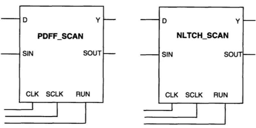
* Cell copies scanned-in data to current state when scanning operation is finished. The control signals for the PDFF and NLTCH cells are system clock, scan clock, and mode select (CLK, SCLK, and RUN, respectively). Symbolic representations of the cells are shown in figure 2-4. Complementary clock signals (CLKN and SCLKN) are created internally to reduce the number of signals that require global routing.
Because of limitations of the support hardware that will test the MAP Chip, it is desir-able that scan operations run slower than the normal system clock frequency. The target system clock speed is 100MHz, and scan clock is expected to run at 10MHz. A separate scan clock is used because it allows system and scan clock frequencies to be completely in-dependent. The main drawback is that it requires two gated clock signals to be distributed
D Y PDFF_SCAN SIN SOUT CLK SCLK RUN D Y NLTCH_SCAN SIN SOUT CLK SCLK RUN
Figure 2-4: Block diagrams of PDFFSCAN and NLTCHSCAN
throughout the chip.
Latch designs that used system clock and two independent control signals were also evaluated. This interface reduces the number of time-critical signals that need to be routed. However, it increases the complexity of using different clock speeds for normal operation and scanning.
2.2.3 Implementation
Schematic diagrams of the new latch cells, PDFFSCAN and NLTCHSCAN, can be found in Appendix A. The cells are similar in high-level design, although device sizes are optimized for different functions.
NLTCH_SCAN
During normal operation, data passes from the D input through the complementary passgate when CLK is low. This passgate and the middle inverter form an inverting negative-transparent latch. From the middle inverter, data propagates through the RUN passgate and the output inverter. The passgate to SIN is normally opaque and the passgate between midout and SOUT transparent, thus SOUT is also a negative-latched copy of the D input. NMOS-only passgates reduces the number of control signals within the latch cells. The passgates at the D and SIN inputs are complementary because node 'midin' is dynamic. Good signal transmission for both high and low values is necessary to create rail-to-rail voltage swing at this node. Use of a PMOS pass device with keeper would provide the same functionality, but also allow the the cell to drive a signal backwards through its unbuffered
T
1CK
Figure 2-5: PMOS with keeper vs. complementary passgate inputs. These circuits are illustrated in figure 2-5
During scan, the D input passgate and Y-output passgate are opaque. The output inverter and feedback inverter are isolated from the rest of the cell, and the Y-output retains its last valid data value. The SIN passgate and middle inverter form a negative-transparent latch, controlled by SCLK. The SOUT passgate and the SOUT output inverter form a positive-transparent latch controlled by SCLK. The latch cell acts as a positive edge-triggered flip-flop for the scan path.
PDFFSCAN
In the PDFFSCAN cell, the D and SIN passgates and middle inverter form negative-transparent latches controlled by CLK and SCLK, respectively.
The passgate between the middle inverter and the output inverter forms a positive-active latch, controlled by a gated clock signal. During normal operation, RUN is high and the passgate is transparent when CLK is high. RUN is held low during scanning, the passgate remains opaque, and the output inverter and keeper are isolated from the rest of the cell.
Use of a CLKA-style circuit to gate the system clock instead of a standard AND gate significantly reduces the propagation delay of PDFFSCAN. For comparison purposes, sim-ulations were run with input signals having 400ps edge times. The CLKA used in the PDFFSCAN cell has a propagation delay for CLK of 60ps. This compares to over 200ps for a NAND gate and inverter.
In PDFFSCAN, the inverter that creates CLKN is asymmetric because the critical transition is CLKN falling. Reducing the size of the PMOS transistor also reduces the clock load of the register.
CTRL
CLK GATED CLK
CLOCK r - GATED
jCTRL:. CLOCK
CTRL V7,/
I-Figure 2-6: Two methods for generating a gated clock.
2.2.4 Usage
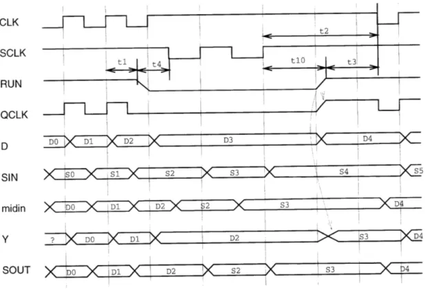
The PDFF and NLTCH cells share the same control signals. For normal operation, SCLK and RUN are held high while CLK toggles. SOUT will follow node 'midin', which is a negative-latched version of D.
In scan mode, CLK is held high. SCLK toggles, and RUN is low to isolate the Y-output from the rest of the circuit.
To change from normal to scan mode:
* CLK stops in and remains in the high state.
* RUN remains high for at least Tcq after the last rising edge of CLK, then falls. This
delay allows the correct data value to propagate to X before the RUN passgate closes. * After RUN falls, SCLK falls. Data from the scan path propagates to the middle
inverter.
* At least one SCLK period after the last falling edge of CLK, SCLK begins to toggle.
(constraint for NLTCH_SCAN) To change from scan to normal mode:
* SCLK stops and remains in the high state.
* RUN rises. Y changes immediately to reflect the last scanned value.
* At least one SCLK period after the last rising edge of SCLK, CLK begins to toggle.
The value at SOUT changes immmediately after the falling edge of CLK.
The maximum idle time for the latches is determined by the charge storage properties of the dynamic nodes, and the required level of noise immunity. Figures 2-7 and 2-8 illustrate the timing of the new latch cells.
D3
D4
SIN Xso
X
siX s2 3 S4 S5midin DO Dl D2 2 DS3
i
D2 %
SOUT
X'DOX
Dl D2 S2 S3 X 4Figure 2-7: Timing diagram for PDFF_SCAN
CLK SCLK RUN midin X Do
IDGX Z2 u IX
D3 S3 OY DO DI D2 S3 D4 t8SOUT
DO2 2 3 D4Figure 2-8: Timing diagram for NLTCHSCAN
RUN QCLK
t6~
s :I
t
iy
? iX DO
DI
S3
D
4D
SIN
S
5
X
4S
ýs iS~
QCL
XD XD
...
CLK Din Vdd "GND" .6v .0v +0.3v -0. 3v 4. o ns
Figure 2-9: Typical waveforms for noise testing
2.2.5
Function
Simulations were initially performed on schematic netlists of the latches. As layout was completed, many tests were repeated using netlists with extracted capacitances from layout. The cells were optimized for performance at TTL conditions (typical NMOS, typical PMOS, Vdd=3.0v). In addition, they were tested for functionality at the other process corners (SS, SF, FS, FF). The following configurations were checked for ****************** race-through and for proper functionality at the process corners. Both data and scan paths
have been checked for each configuration.
* Three PDFFSCANs connected in series.
* A shift-register consisting of seven cells in series: PDFFSCAN, NLTCH_SCAN,
PLTCH, NLTCH.SCAN, PLTCH, PDFFSCAN, PDFFSCAN.
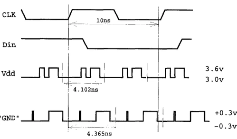
Noise
The seven-cell shift register described above was tested with noise added to ground and Vdd. Clock and data inputs were driven so that each register stage would toggle every clock cycle. Meanwhile, various step-function noise was added to Vdd and ground. The simulation was run for approximately 200 clock cycles, and the output checked for signs of failure.
simulations:
* DATA with f=111MHz; 300mV noise on Vdd, 300mV noise on GND - pass
* DATA with f=111MHz; 325mV noise on Vdd, 350mv noise on GND - fail
* SCAN with f=100MHz; 200mV noise on Vdd, 200mV noise on GND - pass
* SCAN with f=100, 80, 66MHz; 300mV noise on Vdd, 250mV on GND - fail
Power
HSPICE simulations were used to estimate power consumption by measuring the amount of current drawn from the positive supply. Values for typical process conditions and nominal supply voltage (TTL) are shown below.
Input Load
The PDFFSCAN and NLTCH_SCAN cells were designed to have small input loads. This reduces the demand on the MAP chip's clock distribution system. The table below provides
a comparison between obsolete scannable latch cell designs and the final cells used in the MAP Chip.
Cell 0-1 (pJ) 1-0 (pJ) toggle @ 100 MHz (uW)
PDFFSCAN 2.2 1.6 190 NLTCHSCAN 2.2 1.6 190 Cell CLK D SCLK SIN PDFF (old) 39fF 53fF - 6fF PDFFSCAN 27fF 20fF 8fF 15fF NLTCH (old) 28fF 41fF - 37fF NLTCH_SCAN 22fF 33fF 8fF 21 fF
2.2.6
Evaluation
Optimization techniques such as diffusion-sharing and transistor folding were used through-out the physical designs of the latches. The extensive use of passgates reduces the potential for diffusion-sharing, and also increases the complexity of wiring.
The new scannable latch cells incorporate more devices than their predecessors, and are also slightly larger in size. All cells conform to M-Machine standard cell design conventions. Transistor counts and cell sizes are listed below:
Timings
To guarantee correct operation, timing constraints exist for some operations of the latch cells. These are described in the following table. Symbols refer to the indicated locations in figures 2.7 and 2.8.
Symbol Description Min. Timing
ti PDFF: Last CLK rising edge to RUN falling greater than maximum Tcq
t2 PDFF: SCLK rises to first CLK falling edge 1 SCLK period
t3 PDFF: RUN rises first CLK falling edge 1 CLK period
t4 PDFF: RUN falls to SCLK falls Ops.*
tl0 PDFF: SCLK rising edge to RUN rising edge greater than maximum Tcq
t5 NLTCH: CLK rises to SCLK falls greater than maximum Tcq
t6 NLTCH: CLK rises to RUN falls greater than maximum Tcq
t7 NLTCH: RUN rises to CLK falls Ops.
t8 NLTCH: SCLK rising edge to CLK falling edge 1 SCLK period
t9 NLTCH: SCLK rising edge to RUN rising edge greater than maximum Tcq
* Note that to prevent contention, CLK and SCLK cannot both be LOW simultaneously.
Cell Transistors Width (tracks)
PDFF 20 18
PDFFSCAN 23 19
NLTCH 16 16
edge that data must be stable so that the clock-to-q delay is less than or equal to Tcqmin + 15ps. This definition is consistent with M-Machine circuit design conventions.
The sum of setup and propagation time is a measure of a register's overall performance, since circuit design can change how the total delay is divided between these two quantities. The following table lists the setup and propagation times for the new cells.
All HSPICE timing measurements are made with the following configuration, unless otherwise noted:
* TTL process corner.
* 90fF load on Y, to simulate four medium-sized gates (4*INV_2). * 40fF load on Sout.
* All signals measured at 50% points.
* inputs driven by voltage sources with 400ps edge times.
Cell Transition Ts (ps) Tcqmin (ps) Best sum Ts+Tcq (ps)
PDFFSCAN data 0-1 430 510 280+590=870
PDFFSCAN data 1-0 130 680 140+680=820
PDFFSCAN scan 0-1 540 480 400+570=970
PDFFSCAN scan 1-0 310 770 290+790=1080
For negative latches, Tdq is the time necessary for a change in input data to propagate to the output while the latch is transparent. Ts is the minimum time before the rising edge of CLK such that the data-to-output delay of the latch is less than or equal to the minimum Tdq + 15ps.
Cell Transition Ts(ps) Tdq (ps)
NLTCH_SCAN data 0-1 350 640
NLTCH_SCAN data 1-0 180 640
Edge times and propagation delays for NLTCH_SCAN at various process corners are shown below. Tcq is the delay between the falling transition of CLK (50%) and the change
in Y to 50% if the input data changed long before the clock edge. For the scan path, Tcq is the delay between the rising edge of SCLK and the corresponding change in SOUT. Tdq is the delay between changing input data and the corresponding change in Y, when the latch is transparent. All times are measured in picoseconds.
Process corners are represented by two or three letter abbreviations where the first letter represents the NMOS device, the second represents the PMOS device, and the third represents power supply voltage (F=fast, S=slow, T=typical, L=low voltage). Power supply voltage is 3.3v for TT, 3.6v for FF, and 3.0v for FS, SF, SS, and TTL.
Cell Pin Load Corner Tr Tf Tcq01 Tcql0 Tdq01 TdqlO
NLTCH_SCAN Y OfF FF 160 100 290 250 310 170 FS 170 160 500 410 390 390 SF 180 540 500 710 520 620 SS 240 270 710 730 630 640 TT 150 170 460 420 450 380 TTL 180 190 500 460 480 430 90fF FF 260 220 360 320 400 260 FS 550 330 720 550 610 530 SF 370 960 640 1090 690 1010 SS 610 740 930 1060 870 980 TT 410 380 620 550 620 530 TTL 460 470 690 640 660 600 180fF FF 440 290 440 380 500 320 FS 900 400 890 610 780 610 SF 560 1350 760 1420 790 1340 SS 950 1120 1120 1340 1050 1260 TT 650 580 740 670 730 650 TTL 690 660 820 790 790 750
FS 1110 440 570 400
SF 630 2500 310 1580
SS 1120 1500 650 1220
TT 730 710 390 620
TTL 790 840 460 720
The corresponding measurements for PDFFSCAN are shown below.
Cell Output Load Corner Tr Tf Tcq01 TcqlO0
PDFFSCAN Y OfF FF 130 180 150 220 FS 180 220 250 280 SF 170 610 370 790 SS 220 350 470 670 TT 130 260 300 390 TTL 150 260 320 460 PDFFSCAN 90fF FF 300 300 260 330 FS 570 320 470 410 SF 390 1170 520 1300 SS 620 880 730 1080 TT 410 470 460 570 TTL 450 550 510 680 PDFFSCAN 180fF FF 460 410 350 400 FS 980 440 670 510 SF 580 1680 630 1750 SS 1010 1360 930 1430 TT 690 660 600 720 TTL 740 800 660 860
WRITE READ
Figure 2-10: Six-transistor SRAM Cell.
Cell Output Load Corner Tr Tf Tcq01 TcqlO0
PDFFSCAN SOUT 40fF FF 530 410 210 370 FS 1160 440 600 410 SF 690 2860 310 1660 SS 1180 1580 670 1280 TT 770 730 400 650 TTL 830 890 470 750
2.3
Register Cell
2.3.1
Background
The MAP chip contains modules with a wide range of information storage needs. When few bits need to be stored, standard-cell registers may be used. This is easy to design, but is costly in terms of circuit area. For very large arrays such as the on-chip L1 cache, SRAM arrays and analog support circuitry are used. SRAM-based arrays approach allows very dense information storage, but involves analog design. As an intermediate solution for small arrays, a register cell has been designed.
The register cell is a six-transistor cross-coupled inverter circuit, typical of ASIC memo-ries [10]. In the MAP chip, it will be used as a two-port (one write, one read), single-ended cell. The write-bit lines are driven by standard cell inverters. During reads, bit-line voltage swing will be approximately 2 volts, and a ratioed CMOS inverter will sense the state of the bitline. The physical layout will follow standard cell conventions to ease the design of the arrays.
16 cells
144um
YL1
Figure 2-11: Arrays of the register cell used in queues.
2.3.2
Design
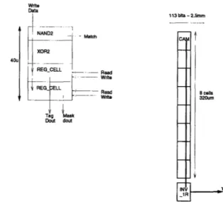
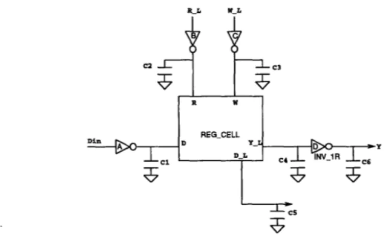
The message subsystem of the MAP chip includes register files and queues which are im-plemented as memory arrays. The storage element for these arrays is the register cell (REG_CELL), a six-transistor static latch configured with single ended read and write ports. The cell is shown in figure 2-10.
The SRAM cell is asynchronous, responding immediately to the control signals read and write. When WRITE is asserted, the the value held in the cross-coupled inverters is forced to the value at input pin D. This assumes that the D input is driven strongly by low-impedance devices. When WRITE is deasserted, the cell will hold its current value. To read the value from a cell, READ is asserted, allowing the cell to drive the bit line. When
READ is deasserted, the output is in high-impedance state.
In addition to a tri-state output, the register cell also has a pin allowing access to an internal storage node. This is used in the GTLB array to support logic for pattern-matching.
Note that adding capacitive load to this node may increase the time needed to write to the register cell.
The register cell is used in several different systems, including the GTLB, network input and output queues, network router, and event queue. In all of these arrays, the register cell drives a capacitive load of approximately 80fF, consisting of interconnect, drain, and input gate capacitance.
Write Data 40u 113 bits - 2.5mm Match CA A - Read Write Read 8 cells Write 320um
Figure 2-12: The CAM cell and its arrangment in the GTLB.
2.3.3 Implementation
To simplify physical implementation, the register cell layout is designed using MAP chip standard-cell conventions. It is five tracks wide to accomodate its five signal pins. Signal pins are arranged so that each signal can be assigned to a seperate horizontal and vertical track. The output is single-ended and will be sensed by a standard CMOS inverter.
Initial estimates indicated that the driving inverter should have an NFET of approxi-mately 3.5, with balanced PFET. Assuming that the READ pass transistor is also 3.5, the worst-case total output load for a 16-cell bitline is 73fF.
Based on the approximation of an ideal fanout of 3 (e=2.7), the driving NFET should have a width of roughly 4-5. In the layout, there is sufficient area for a 3.7 NFET. The width of the PFET is equal to that of the NFET to reduce the switching voltage of the inverter. This is necessary because signals from the input pin passthrough an NFET device and range between ground and Vdd-Vtn. The keeper inverter is implemented as a minimum-size PFET and a minimum width, double length NFET.
Increasing the width of the output pass transistor can improve the read-out speed. How-ever, because a significant part of the bit line load capacitance consists of drain capacitance of these devices, the improvement is small.
Read time is reduced significantly for the '0' case by using a sense inverter (INV_IR) with reduced threshold voltage instead of a standard INV_1. Results of HSPICE simulations
2.3.4
Evaluation
The Cell
The times below are measured with HSPICE at TTL conditions for the circuit in figure 2-11. Inputs are driven by voltage sources with 400ps edge times. Propagation times are from READ signal rising to 50% to the Y output reaching 50%. A capacitive load of 45fF is placed on the output of the sense inverter to simulate a fan-out of four. The sense inverter is a modified INV_1 cell, with PMOS=2.5um, NMOS=5.5um.
Output device size Total output load Tpd 0-1 Tpd 1-0
3.7um
70fF
680ps
740ps
The times necessary to write to the cell are shown below. Because of feedback from the keeper-inverter, the load on pin DIL affects the time necessary to write the cell. These simulations were run at TTL conditions, with inputs driven by voltage sources with 400ps edge times. Times are measured from WRITE rising to 50% to the voltage at node x reaching 80% of its final value. Times are measured to node x reaching 80% of final value instead of the midpoint in order to guarantee that the cell will remain stable with the correct
data value.
D_L load write 1 write 0
OfF 930ps 180ps
10fF 1030ps 180ps
20fF 1120ps 180ps
50fF 1390ps 180ps
100fF 1780ps
180ps
When READ is asserted, charge sharing with the bit line causes a voltage spike to appear on the D_L node. At TTL conditions with 70fF of load from the bit line, the '1' voltage dips to 2.2 volts, and the '0' voltage peaks at 0.5v. The keeper inverter has a threshold of
Vdd/2 = 1.5v, so noise margins are acceptable for both cases.
In the extreme case, a large bit line load could cause the cell to change state. At TTL conditions with no external load on DIL, this occurs when the bitline load exceeds 600fF. Thus, the maximum safe load is much larger than the load of the arrays.
The table below lists the register cell's performance with varying process conditions. The simulations reflect the configuration shown in Figure 2-11, and measure from READ rising to 50% to Y output reaching 50%.
Corner Vdd Read 1 Read 0 Write 1 Write 0
FF 3.6v 440 ps 330 ps 410 ps 80 ps FS 3.0v 800 400 680 90 SF 3.0v 510 1300 1460 240 SS 3.0v 810 1100 1470 200 TT 3.3v 630 610 780 160 TTL 3.0v 680 740 930 130
The driver inverter is ratioed for a reduced switching threshold. This improves speed by adjusting the threshold to meet the limited voltage output of the NMOS passgate. With a balanced 2/1 ratioed inverter, the cell fails to write a '1' at the slow-N fast-P process corner.
Arrays: Queues
Simulations were performed using driver and receiver circuits, a single active register cell, and capacitive loads to model the the rest of the network queue. The arrangements shown in figures 2-11 and 2-12 were evaluated with standard cell inverters of various sizes used to drive control and data inputs to the array.
The following capacitances were used in the array model to simulate the network input queue, which has the largest capacitive loads of the queue-type structures:
Name Description Total (fF)
C1 write-bit line 210 C2 write control 625 C3 read control 650 C4 read-bit line 75 C5 Y output 45 C6 DL load 0
The estimate for C1 assumes that all write-bit together and driven by the same inverter.
Figure 2-13: Model for capacitive load of arrays.
Data and control inputs to the register cell array are driven by standard cell inverters. For the queues, the following sizes were used. Propagation time is measured from when the input signal reaches 50% (Vdd/2) to the output reaching 50%.
The following simulation results were obtained using otherwise noted.
the conditions listed below, unless
* TTL process corner, Vdd=3.Ov
* Inputs (Din, RL, WL) are voltage sources with 400ps edge times. * Layout parasitic capacitances (lpe) are included in the HSPICE models.
Setup time (Ts) is the minimum time between D becoming stable and the falling edge of W to guarantee correct data is written to the register cell. This is measured from D reaching 80% of its final value to W reaching 50%, as shown in figure 2-14. For the queue
array, the worst-case setup time (write '1') is 600ps.
Read time is the time between R being asserted and the correct data value appearing at the array's Y-output, measured from R reaching 50% to Y reaching 50% of its final value. Read times are 830ps for '0' and 700ps for '1'.
Inverter Standard Cell(s) Tpd
A
INV_2
450ps
B INV_8 380ps
D
Figure 2-14: Setup time for register cell
RL
R
VALID
Tr
Figure 2-15: Read time for register cell
2.3.5
Arrays: GTLB
The following capacitances the GTLB.
were used in the array model to simulate the CAM cell array in
Inputs to the arrays are driven by scaled inverters with the following sizes. Inverters for the read and write control signals are connected in parallel to increase drive strength.
Name Description Total (fF)
C1 write-bit line 80 C2 write control 1050 C3 read control 1090 C4 read-bit line 80 C5 Y output 45 C6 DIL load 18
5.5
Figure 2-16: Schematic for INVI1R.
In the GTLB configuration, the minimum setup time is 570ps. Read times for '0' and '1' are 1150ps and 1060ps, respectively.
2.3.6
Low Threshold Inverter
An inverter with reduced switching voltage is used to sense the state of the read-data bitline. All standard cell inverters are sized for a Vdd/2 switching threshold, however the register cell's NMOS-only passgates do not create full-swing output signals. To improve speed and tolerance to process variations, a new cell was created. The new cell, INV_1R, has comparable drive strength to an INV_1, but a lower switching threshold. Its physical design is a simple modification of the INV_1 layout, thus pin locations and overall size are identical.
The new ratio of device sizes results in a threshold of approximately 1.1v at TTL condi-tions, compared with 1.5v for standard cell inverters. At varying process corners and power supply voltages, the threshold voltage changes as listed below:
INVERTER TEST TTL 96/o, Ji z - 17 !EG t : "" • ... i
~...
... ... ... . . .- • V _ T . W --... ... --- --- ... - - .... . . ... ... - . . ... . . . -. .. . .. .. . .. . . _ . .. . .. . .. .. . .. ..: ... . .. . .. . .. . .. . .!. .. . . .. . . .. . ... - . . . .. . . .. .. . ..:~~~ i i : ... ... ... -... \. ... ... : ... .... ::... . . ... .... ... -_--... ... ... ... ... ... -- - - - ---- ... . ..i ... ... •... ... .- .. • .... ... i... ... zj-
.
...
.
i...
...
i
...
..
...
!
...
...
r····- ·· · · ·· ·: ---··-·---- ----·.~
· · ·-- ·· -- ... ... . . .... ... . ...... ... :~..,..~... ... ,~~,~~,~~.~~i... .. ... 3L... ..- L_ : _ ... ... ... ... i . ... ... ... ... ::... ... ...".:-
...
...
..
...
...
.
....
...
...
...
:...-.
......
....
-- . . . ..:.. ... .. ..:... . .-...,,... ...- ... -500 Oa 1 0 5IN 2 0 2 50 VOLTS (LIN) 3.0 2.80 2.o0 2.20 * .40 1.60 1.20 1.0 800. O GOO.OM 00 . O 200 OM 0Figure 2-17: Transfer curve for INV_1R at TTL conditions.
2.3.7
Summary
Based on the specifications in CVA Memo #90, "Datapath Proposals for GTLB, NETOUT,
NETIN, ROUTER, AND EVENTQ," a physical design for the register cell has been created. A standard cell inverter layout has been modified to produce a sense-inverter with reduced
threshold voltage. Layouts have been verified using standard simulation and verification
tools.
Corner Vdd (volts) Vt (volts)
FF 3.6 1.22 FS 3.0 0.88 SF 3.0 1.38 SS 3.0 1.20 TT 3.3 1.25 TTL 3.0 1.18
0.3x lx
Figure 2-18: weak NAND, AND with buffer, and proposed NAND_2.
2.4
Logic Cells
The original standard cell library used to synthesize logic for the MAP chip includes logic gates in only one device size. Only inverters and tri-state inverters are available in a variety sizes to drive large loads. When large fan-out nodes or long runs of interconnect occur, large sized inverters are used to drive the loads. Available sizes for inverters are lx, 2x, 4x,
and 8x, where 1x is the standard output drive of a logic gate with a fan-out of four. Not all logic gates have full output drive (lx). Due to size and input load constraints, some gates have as little as half of normal output drive. If an output must drive several other gates, it must be buffered using inverters.
An example of buffering using inverters appears in figure 2.18. Suppose the desired
out-put is Y = NAND(A,B). The leftmost picture shows the one-cell implementation (NAND2),
which has inadequate drive strength. To remedy this, the NAND gate is implemented as an AND gate and a 2x inverter added as shown in the center. Note that this requires three stages of logic, a large increase from the single-stage NAND gate.
Use of logic gates with larger device sizes can result in significant reductions in propa-gation delay and/or area. Three double-sized logic gates were designed: two-input AND, NAND, and NOR gates.
The table below lists propagation delays for a ix-sized inverter driving the logic gate under test and a 20fF load to represent other gates or interconnect capacitance. The gate+inverter combination or 2x-sized gate drives a load of 90fF. Refer to figure 2-19 for a diagram of the test circuit. A plot of the circuit used for timing measurement is included in the appendix. The input load for double-sized gates is double that of the lx gates. The increased input capacitance affects the propagation delay of the previous output stage, as shown below.
r---.
Gate or
1x >0 undertgate + inverter '-- I test
20 f L0 f
Figure 2-19: Circuit to evaluate logic gate propagation delay.
Logic Inverter Tpd Logic gate Tpd Total
NAND + INV_2 185ps 525ps 710ps
AND 2 190ps 545ps 735ps
AND + INV_2 170ps 640ps 810ps
NAND_2 250ps 2 70ps 520ps
There is little timing difference between the AND_2 and NAND+INV_2. In contrast, the NAND2 provides a significantly lower delay than the AND+INV_2 combination. This is because the NAND gate contains only one stage of logic while the AND+INV_2 has three: a NAND gate and inverter to make an AND gate, and the 2x-sized inverter.
The double-sized logic gates also use less area than a combination of gate and inverter. This is caused by better device sizing, and efficient physical design. Standard cells have uniform heights, therefore area is proportional to their widths, measured in tracks. The 2x-sized cells are 16% to 37% smaller than the gate+inverter combinations that they replace.
Circuit Width (tracks)
NAND + INV_2 6 AND_2 5 AND + INV_2 8 NAND2_2 5 OR2 + INV_2 8 NOR_2 5
Based on the above results, 2x-sized logic gates provide a significant reduction in prop-agation delay and/or area when they can be used. Their major drawback is that input capacitance increases proportionately. The NOR_2 has nearly 3x input capacitance, and may require buffering of the previous logic stage. The OR_2 gate was not implemented because the expected benefits are small, similar to the AND_2.
sized inverter. These macros have the same area and delay characteristics as the sum of the cells they include, and are primarily intended to aid in the automatic synthesis of standard cell logic. Macro-cells which incorporate a latch and multiplexers have also been designed to simplify logic synthesis.
Chapter 3
Clock Distribution
3.1
Introduction
The MAP Chip accepts a differential clock reference signal from an external source, dis-tributes differential signals throughout the chip, and uses these to create ended single-phase clock signals for use in its modules. Three levels of differential-in differential-out buffers (DIDOs) and interconnect transmit the differential signals to differential-in single-ended-out pulse generators (DISOPGs), which drive local CLK and CLKL loads.
3.2
Design
3.2.1
Overview
The clock distribution system is organized as follows:
* Level 1: Two DIDO buffers located at the center of the chip. One drives the horizontal
distribution tree for the left half of the chip, the other supplies the right half.
* Level 2: Sixteen DIDOs organized as eight pairs, evenly spaced on a horizontal line
along the center of the chip. Each buffer drives a vertical distribution tree for either the top or bottom half of the chip.
* Level 3: Sixty-four DIDOs arranged on a grid with approximately 2mm spacing. Each L3 may drive up to twelve pulse generators (DISOPG). The load on L3 buffers may
LEVE\
LEVEL3
.
and
CLK L
LEVEL2a I /I CLK
N GENERATOR .
LEVEL
Figure 3-1: Global Clock Distribution.
* Level 4: Differential-in Single-ended out Pulse Generators (DISOPG), each driving
up to 5pF of clock load. Pulse generators are used instead of standard buffers to avoid large short-circuit currents. DISOPGs with reversed differential inputs will be used to generate CLK_L.
* The outputs of all DISOPGs for CLK are tied together into a global clock grid to
reduce skew. Likewise, CLK_L outputs are connected into a global CLK_L grid.
* The total CLK load of the MAP Chip is estimated to be lnF. The CLK_L load is
estimated to be 0.4nF Note that clock load density varies greatly across the chip.
3.2.2
Wires and Wire Models
Tree structures are used to transmit differential clock signals throughout the chip. A tree is illustrated in figure 3-2. This structure guarantees that all receiving nodes are equidistant from the transmitting node, thus minimizing skew due to varying propagation times.
Interconnect capacitances were estimated using process design information. Assuming that the routing in adjacent metal layers is perpendicular (Ml vertical, M2 horizontal, etc), there is a maximum of 50% coverage for up and down capacitances. Fringe and line-to-plate capacitances are scaled accordingly.
The horizontal and vertical trees will run in the two topmost metal layers, consistent with the MAP routing conventions. The horizontal distribution trees may be implemented
driver 4.5mm
2.25mm
1.125mm
receivers
hA
t
Figure 3-2: Clock Distribution Tree.
with minimum-width wires. The vertical trees will be triple-width (2.7um) wires. This reduces wiring resistance by a factor of three while increasing capacitance by only about one-third, thus reducing interconnect RC delay. The results are shown below. The total capacitances include input capacitance of the next-level driver. Ideal edge time is to the time for the receiver node to change from 20% to 80% of its final value when a step input is applied to the top of the tree.
Wire type Width Ideal edge time
LM 1x 220 ps
M4 lx 1700 ps
M4 3x 510 ps
Each Level 3 DIDO distributes the clock reference signals to up to twelve DISOPGs within a 2mm square area. Each DISOPG drives up to 5pF of load. An estimate for
maximum L3 wire length is 12*v2'/2 = 8.4mm, and the total load for the L3 DIDO is
1.8pF.
3.2.3 Differential Buffers
General Design
The three levels of DIDOs will all use the same buffer circuit. Representative waveforms for the differential clock distribution system are shown in Figure 3-3.
The DIDO consists of three stages: a modified Chappell amplifier and two Hartman-type buffers of increasing size. The Chappell amplifier stage [2] is used for its large differential gain and common-mode rejection. A variation of the Double Mirror-Compensated CMOS ECL Receiver designed by Chappell is used as differential receiver in the DIDO. The differ-ential input signal is supplied to the gates of the NMOS input devices. The bias voltage for
DIDO1
neg. output DIDO2
DIDO3
Figure 3-3: Ideal Waveforms for DIDO
each side of the amplifier is the output voltage of the other half. The P-channel load de-vices are in mirror-bias configuration. During a transition, the bias voltage of a half-circuit changes, causing the PMOS load device and NMOS current source to change their transcon-ductances in the direction to improve the differential gain. The circuit is self-biased with both PMOS and NMOS load devices, and provides good compensation to power supply and P/N device common-mode variations.
The Hartman buffers, also known as Push-Pull Cascode Logic [5] include cross-coupling to maintain the complementary properties of the differential signals. The two stages increase in size to provide adequate drive current for large capacitive loads. The second stage is also sized to provide similar output rise and fall times.
The Hartman differential amplifier is designed to provide fast worst-case edge times. It uses NMOS devices to provide most of the switching currents, and cross-coupled PMOS devices to provide full- swing outputs. For example, when the positive input rises from ground to Vdd and the negative input falls to ground, NMOS transistors pull down the negative output and pull up the positive output. Short- circuit current flows until the opposite-polarity NMOS devices are completely turned off. When the negative output falls below Vdd-Vtp, a PMOS transistor turns on and helps to pull the positive output to Vdd. The final stage Hartman amplifier is sized to provide similar rise and fall times. In this arrangement, the pull-down NMOS and pull-up PMOS devices are provide most of the current for transitions. The pull-up NMOS devices are small to reduce the input load of the buffer.
currently sized, the unloaded buffer has equal edge times. When loaded with 1.8pF to 4pF, edge times are nearly equal.
Sizing
The DIDO is designed to drive a load of 4pF, which corresponds to a triple-width wire tree as described in the previous section. The edge time requirement is flexible for the DIDO because of its analog nature. The maximum edge time is set by the required level of noise tolerance. The DISOPG will function with edge times greater than one nanosecond (see following section). A schematic for the DIDO can be found at the end of this document.
The second Hartman stage consists of 120-wide NMOS devices to drive a 4pF capacitive load. The approximation that an NMOS device drives ten times its own width of gate suggested that the first Hartman stage should be 24um wide. The Chappell amplifier was then sized to drive the input load of the first Hartman stage. The second Hartman stage was resized to provide similar output rise and fall times.
3.2.4 Pulse Generators
General Design
The pulse generator accepts a differential reference signal and generates a single-ended system clock that can drive up 5pF of load with 400ps edge times. Pulse generators are used instead of conventional buffers (inverters) to reduce the amount of short-circuit current caused by the large output driver stage. The polarity of pulse generator differential inputs can be reversed to produce either CLK or CLKL.
The differential amplifier accepts a differential clock reference signal and creates a single-ended output. This is buffered by a series of inverters which drive the pulse generator.
The pulse generator controls its output drivers based on the difference between its input signal (pg-in) and a delayed and inverted version of it. At DC, the output drivers are off and a small keeper maintains the proper voltage level for CLK. When pgin transitions from low to high, both the input and delayed signal are high for a period determined by the delay chain. This is detected by the NAND gate and used to turn on the PMOS output driver, causing CLK to rise. Likewise, when pg in falls both it and the delayed signal are low. This is detected by the NOR gate and turns on the NMOS output driver, pulling CLK
Delay_n
up_n
down
CLK
Figure 3-4: Ideal Waveforms for DISOPG
low. This is illustrated in Figure 3-4.
Sizing
The large output driver devices were sized to provide 400ps edge times on the CLK signal. HSPICE measures 430pS rise time and 390pS fall time on CLK. The high and low times are closely balanced, as HSPICE measures 4.97ns high time (CLK 50% to 50%). Times in this section are measured with 5pF load on CLK, and differential inputs driven by standard cell INVI's.
The NAND and NOR gates are sized to drive these large devices with fast rise/fall times for critical edges (upn Tf=320ps, down Tr=350ps), and slow transitions for non-critical edges. The transistors active in the non-critical edges are sized asymetrically, with the early-arriving signal (d3n) controlling large transistors and the late arriving signal (pgin) controlling smaller devices closer to the outputs. The slow-transition devices were sized to keep the voltage change of upn and down from the supply rails due to capacitive coupling
at less than 200mV.
The keeper inverters maintain CLK at full-swing voltages when the driver transistors are off. With 5pF of clock load, the CLK signal will change less than 0.5v with up to 1pF of capacitive coupling between CLK and a full-swing signal with 300ps edge time.
The delay chain consists of three inverters. At TTL conditions, the width of up_n pulse was measured to be 1.6ns (50% to 50%), or 760ps (10% to 10%). The down pulse was measured to be 1.8ns (50% to 50%), or 790ps (90% to 90%).
In the worst case process corner (FF), The upn pulse remains below 10% for 260ps after CLK rises to 90%. Down remains above 90% for 280ps after CLK falls to 10%.
The pulse generator is sensitive to the edge times of pgin, since slow edge times affect the edge times of the pulses and cause slower edge times on CLK. Edge times of pgin were measured to be Tr=370ps, Tf=320ps.
The DISO amplifier converts a full-swing differential signal to a full-swing single-ended signal. High gain is not required. The circuit was sized to provide reasonable edge times (Tr=420ps, Tf=300ps) and propagation delays. The following inverter is sized to correct for the rise/fall time asymmetry of the differential amplifier. This inverter is also a convenient way to fine-tune the duty cycle of CLK.
3.3
Sources of Clock Skew
Temporal differences between the clock signals in different parts of the chip is caused by many factors. Some important ones are described below, along with possible ways to tolerate or compensate for them.
Power supply variation, either local or chip-wide, causes skew between single-ended signals by creating a difference between transmitter and receiver switching thresholds. The use of differential circuits with common-mode rejection and are less affected by changes in the power supply.
The L3 DIDOs may have different loading because of varying numbers of pulse gen-erators in a given area. This changes the amount of interconnect capacitance, and thus the propagation delay between the L3 DIDO and connected DISOPGs. This effect can be lessened by controlling the total number of pulse generators connected to each L3 buffer. Extra wires or capacitors can be added to equalize the loads seen by the third level DIDO. Process variation can influence the properties of both devices and interconnect. Simula-tion has been performed to examine system behavior with device variaSimula-tion. If interconnect properties exhibit large process variation, multiple wire models could be created to represent the different conditions.
The length of interconnect between DISOPG output grid and where CLK is used can vary. In addition, the load on DISOPGs may vary. These can be controlled by careful layout and routing.
The following sections describe the circuit-level simulations done during the design of the clock buffers. Detailed analysis which includes extracted layout capacitances is being per-formed as the physical design is completed. Detailed chip-wide evaluation using RC and transmission line models to evaluate skew is also in progress.
3.4.1
Differential Buffers
The following table shows the expected performance for the DIDO circuit driving a triple-width distribution tree, corresponding to a 3.9pF load. Devices are typical-N, typical-P, with a 3.0 volt power supply ("TTL" conditions).
All edge time measurements are from 20% to 80% of the final output value. Nodes cp, hip, and outp refer to the output nodes of the three differential amplifier stages, as shown on the schematics in the appendix. Node 'leaf' is one of the leaf nodes in the clock distribution tree. Measurements at this node represent the input signals to the next-level differential
receivers. Thigh is the period between the 50% point of the signal's rising transition to the
50% point of the falling transition.
Node Trise Tfall Thigh
cp 510ps 400ps
hip 380ps 350ps
outp 550ps 460ps 4.88ns
leaf 750ps 670ps 4.86ns
As noted above, the relative rise and fall times of the DIDO depend on the load on its output. The level 3 DIDO will drive a capacitive load of up to 1.8pF. The following table lists the edge times for a DIDO at TTL conditions driving a 1.8pF load. As an indication of the optimal performance of the circuit, edge times with no load are also shown.
Load Trise Tfall Thigh
OpF 170ps 180ps 5.00ns
1.8pF 410ps 390ps 4.88ns
To evaluate the noise sensitivity of the DIDO, HSPICE simulations with step changes in power supply voltages were used. Test scenarios included 600mV peak-to-peak noise
VDD INP, INN OUTP, OUTN
1
_
I
!
i
skew 3. 6V 3.3vFigure 3-5: Noise Test Waveforms for DIDO
on Vdd or ground. The DIDO has good immunity to power supply noise. Representative waveforms are shown in figure 3-5.
The crossover point of the differential inputs shifts in time in response to power supply changes. This point is significant because the differential receiver compares the relative voltages of its two inputs. The following table summarizes this shift for a DIDO driving a triple-width wire model (3.9pf). The shift measured at the driver output was within 10ps of the shift at the wiring tree's receiver nodes.
Initial Vdd Initial GND Noise Max. change of crossover
Vdd step to 3.6v
-140ps
Vdd step to 3.0v +160ps
3.3v Ov none Ops
GND step to 0.3v +170ps
GND step to -0.3v -130ps
Measurements of DIDO output currents into its largest expected load, distribution tree, are shown below. These measurements can be used to minimum wire widths and contact quantities to prevent electromigration.
a triple-width determine the
Process Corner Vdd RMS Current Average Current
FF 3.6v 5.1mA 2.4mA
between large input devices for high gain, and reducing the input capacitance. The following table shows the pulse generator's performance with slowly changing input signals. Thigh is
the time between a signal rising to 50% and falling to 50%. Rise and fall times are measured between 10% and 90% points. Times measured at TTL conditions with 5pF load on CLK.
Edge time DISO Thigh (ns) Tr (ps) Tf (ps) CLK Thigh (ps) Tr (ps) Tf (ps)
400ps
4.90
540
340
4.97
435
420
800ps
4.90
610
440
4.99
435
400
1200ps
4.95
620
450
5.03
435
410
1600ps
4.96
690
510
5.07
445
410
The rated clock load for the pulse generator is 5pF, but actual clock load may vary. The following table shows the DISOPG output characteristics with varying clock load, at TTL
conditions. Differential inputs are symmetric with 800ps edge times.
The following measurements reflect the performance process and power supply conditions. Differential inputs times.
of the DISOPG under varying are symmetric with 800ps edge
Load (pF) Thigh (ns) Tr (ps) Tf (ps)
0 4.99 165 215
2.5
4.99
310
315
5.0
4.99
435
400
6.0
5.00
470
460
Process corner Vdd (v) Thigh (ns) Tr (ps) Tf (ps)
FF 3.6 5.18 265 255 FS 3.0 5.16 515 350 SF 3.0 4.97 330 470
SS
3.0
4.85
575
555
TT 3.3 5.02 395 385 TT 3.0 4.99 435 400VDD INP, INN CLK sweep . ske---w-skew 3. 6V 3.3v -•1. 65v
Figure 3-6: Noise Test Waveforms for DISOPG
Noise tests similar to those for the DIDO were performed on the DISOPG. Eight sce-narios were tested: 300mV step change in the up or down direction on either Vdd or GND, with CLK either rising or falling. The voltage step was swept over the period between the DISOPG input starting to change and the output transition finishing, in 50pS steps. Figure 3-6 illustrates typical test waveforms.
Skew was defined as the maximum variation between the time CLK reaches 3.3/2=1.65 volts with a step change in either Vdd or GND, and when CLK would reach 1.65v for a DISOPG with 3.3v constant power supply. The measured skew was between -100ps and
+100ps for all test scenarios.
The output devices of the DISOPG create large currrents. Output wires must be wide enough to prevent electromigration. The following are RMS current measurements at var-ious process corners. Current was measured between the output node of the large load-driving devices and a 5pF load.
3.5
Power Dissipation
The clock distribution system includes many large devices, and has high power dissipation. The DIDO and DISOPG both include differential receiver circuits that dissipate static power. Total clock power dissipation for the chip is 6.2W at fast-N fast-P 3.6v power
Process Corner Vdd RMS Current Average Current
FF 3.6v 14mA 3.8mA