Circuits for High-Performance Low-Power VLSI Logic
by
Albert Ma
Submitted to the Department of Electrical Engineering and Computer Science
in partial fulfillment of the requirements for the degree of
Doctor of Philosophy in Electrical Engineering and Computer Science
at the
MASSACHUSETTS INSTITUTE OF TECHNOLOGY
June 2006
@ Massachusetts Institute of Technology 2006. All rights reserved.
Author
-...... :.
.. ...
Department of Electrical Engineering and Computer Science
May 5, 2006
//
C ertified by ...
J
j
....
•w.
r..
...
Krste Asanovid
Associate Professor
Thesis Supervisor
~-,-Accepted by ...
...
...
ý...~..
...
Arthur C. Smith
Chairman, Department Committee on Graduate Students
OF TECHNOLOGY
ARCHIE8S
NOV 0.2 2006
LIBRARIES
Circuits for High-Performance Low-Power VLSI Logic
by
Albert Ma
Submitted to the Department of Electrical Engineering and Computer Science
on May 25, 2006, in partial fulfillment of the
requirements for the degree of
Doctor of Philosophy in Electrical Engineering and Computer Science
Abstract
The demands of future computing, as well as the challenges of nanometer-era VLSI design,
require new digital logic techniques and styles that are simultaneously high performance,
energy efficient, and robust to noise and variation. We propose a new family of logic styles
called Preset Skewed Static Logic (PSSL). PSSL bridges the gap between the two main
logic styles, static CMOS logic and domino logic, occupying an intermediate region in the
energy-delay-robustness space between the two. PSSL is better than domino in terms of
energy and robustness, and is better than static CMOS in terms of delay. PSSL works by
partially overlapping the execution of consecutive iterations through speculative evaluation.
This is accomplished by presetting nodes at register boundaries before input arrival.
Thesis Supervisor: Krste Asanovi6
Title: Associate Professor
Acknowledgments
I would like thank God for the opportunity He gave me to do this PhD, the strength to
finish it, and the people He gave that supported me all the way. Thank you Krste for your
guidance, patience, and grace. You have done the impossible in graduating me. Thanks to
Srini and Anantha for being on my committee. Thanks to the SCALE group for you help
and support.
I also want to thank my parents, for their sacrifice, love, and support through the years.
Finally, I want to thank my wife Sophia, Pastor Paul, Becky JDSN, Pastor Chris, Sally
SMN, Heechin JDSN, Jean SMN, and all those in the body of Christ who have prayed for
me these ten long years.
This work was partially supported by NSF CAREER Award CCR-0093354, the
Cambridge-MIT Institute award 093-P-IRFT(Cambridge-MIT), PERCS project W0133890, and a donation from
the Intel corporation.
Contents
1 Introduction
2 Background - Scaling and the Challenges for future computing
2.1 Power Consumption ...
2.2 Robustness ...
2.2.1 Signal noise and signal integrity . ...
2.2.2 Single Event Phenomena and soft errors . ... 2.2.3 Variability ...
2.2.4 Improving Robustness
2.3 Conclusion ...
3 Background - Logic Styles
3.1 Static CMOS ... 3.2 Domino ... 3.3 Conclusion ...
4 Preset Skewed Static Logic
4.1 Skewed Static Logic 4.2 Preset . ... 4.3 Unateness ... 4.4 Pipelining ... 4.4.1 Level-sensitive 4.4.2 Edge-triggered 4.4.3 Pulsed ... 4.5 4.6 4.7 4.8
Leakage and leakage variability impact
Variability impact ...
Single Event Phenomena ...
Conclusion ...
5 Previous Work and Comparison
5.1 Logic styles . ... 5.2 Variability . ... 5.3 Pipelining . ... 5.4 Timing Elements . ... 5.5 Conclusion ...
. . . .
.6 Managing Leakage 55
6.1 Leakage ... 55
6.1.1 Multiple-Vth circuits ... ... 55
6.1.2 Sleep Vector technique ... ... 56
6.1.3 Power Gating ... . ... .... 57
6.1.4 Applications to PSSL ... ... 59
6.2 Conclusion ... ... .. 61
7 Evaluation 63 7.1 Linear Feedback Shift Register ... ... 63
7.1.1 Methodology ... .. ... ... 63
7.1.2 Results ... ... .. 64
7.2 Shift register using wide fan-in gates ... ... 64
7.2.1 Methodology ... ... 66 7.2.2 Results ... . ... ... 67 7.3 Flip-flop comparison ... . ... . . 67 7.3.1 Methodology ... ... 68 7.3.2 Results ... ... .. 69 7.4 32-bit Accumulator ... ... 71 7.4.1 Implementation ... . . . .... . 71 7.4.2 Evaluation . ... .. ... .. 72 7.5 Conclusion ... ... . . ... 72 8 Testchip 75 8.1 Architecture ... ... .. 75 8.1.1 Test infrastructure ... ... . 75 8.1.2 Measurement infrastructure ... .... 76 8.1.3 Chip operation ... .... ... .. 77 8.1.4 ALU architecture ... ... . 77 8.2 Implementation ... ... .. 78
8.2.1 Transistor size selection ... ... ... 78
8.2.2 Layout ... ... ... ... 80
8.3 Simulation Results ... .... ... .. 80
8.4 Test and Measurement Methodology ... ... 80
8.5 Conclusion ... ... .. 82
9 Conclusion 83 9.1 Summary of Contributions ... ... . 83
List of Figures
2-1 Major transistor leakage paths . . . . .
3-1 Basic logic styles .. ... ... ... ... ... .. ... ... ... . .
3-2 Domino switching and contention . . . . .
3-3 Sources of noise in domino logic . . . . ...
3-4 Dynamic keeper sizing ...
4-1 Skewed inverter chain energy-delay performance ...
4-2 Preset Skewed Static Logic . . . ... . .. . .
4-3 A 2-input NOR embedded in PSSL preset-high circuitry . ... 4-4 Non-unate logic . ...
4-5 Two stage Level-Sensitive PSSL pipeline and timing diagram... 4-6 Two stage Level-Sensitive PSSL pipeline timing overlapping clocks.. 4-7 LS-PSSL time borrowing. ...
4-8 4-phase LS-PSSL ...
4-9 N-phase LS-PSSL using dynamic preset and clock waveforms ... 4-10 Edge Triggered PSSL and timing diagram . ...
4-11 Pulsed PSSL pipeline with timing diagram . . . . ...
4-12 Gate leakage in the preset state . . . . .
5-1 5-2 5-3 5-4 5-5 5-6 5-7 5-8 6-1 6-2 6-3 6-4 6-5 6-6 6-7 6-8 Conditional-keeper technique. . ... Noise-tolerant precharge . . . . Skewed CMOS pipeline and timing diagram ...
Skewed CMOS vs. LS-PSSL timing charts ... Output Prediction Logic ...
Low Voltage Swing Logic . ...
Process-Compensating Dynamic circuit technique . . . . .
Leakage Current Replica Keeper . ... Static CMOS leakage paths ...
Leakage-proof domino circuits . . . . .
Leakage-Biased Domino ...
Multithreshold voltage CMOS logic . . . . ...
Super Cut-Off CMOS logic. ...
Zigzag Super Cut-Off CMOS logic and leakage paths. . .
Gate-leakage Suppressing CMOS logic . . . .
Comparison of leakage paths in Static CMOS and multi-Vth PSSL. 7-1 Two-bit Linear Feedback Shift Register . . . . .
7-2 Linear Feedback Shift Register implemented using LS-PSSL . ... 64
7-3 Linear Feedback Shift Register energy-delay comparison . ... 65
7-4 LS-PSSL LFSR waveforms ... ... 65
7-5 Four-bit shift register using wide-fan-in gates. . ... 66
7-6 Four-bit shift register energy-delay curves. . ... 67
7-7 Flip-flops for comparison ... ... . 68
7-8 Test-bench setup ... ... . 69
7-9 Energy versus delay for various flip-flops. . ... . 70
7-10 Energy Dissipation across different input waveforms for various flip-flops. 70 7-11 Accumulator design ... ... .. 71
7-12 Adder architecture ... .. ... .. 71
7-13 32-bit accumulator comparison. ... ... 73
8-1 Test-chip block diagram. ... ... 76
8-2 On-chip VCO frequency vs. input voltage. . ... .. 77
8-3 ALU block diagram. . ... ... ... 78
8-4 ALU energy-delay comparison with varying transistor sizes. . ... 79
List of Tables
3.1 Per-input logical effort of common gates . ... . . . . 23
4.1 LS-PSSL Preset latches and their properties. . ... 36
8.1 Testchip ALU size comparison. ... 80
Chapter 1
Introduction
The relentless drive toward smaller, faster, and cheaper computing systems has, in large part, been enabled by exponential increases in device density and operating frequency through VLSI: technology scaling. This, however, has led to exponential increases in power consumption that has reached the limits of reliability and cost effective cooling. In addi-tion, the continued scaling into the nanometer regime has brought with it design robustness issues such as signal integrity, soft error, and environmental and process variability. Fur-thermore, the issues of power consumption and robustness only get worse with time. This has created, therefore, a crisis in computer system design that threatens to be a stumbling block to future advancement.
Designers of leading-edge computing systems, at any scale, are finding that power con-sumption and design robustness are first class constraints, and must be taken into account at every level of design. At the circuit level, the choice of logic styles is important as it directly affects power, performance, and robustness. The two prevalent logic styles, static CMOS and domino logic, do not fully meet the needs of future computing. Static CMOS, though energy-efficient and robust, is too slow to be used in timing-critical designs. Domino logic, though fast, consumes too much power and is not robust. In addition, domino logic scales poorly so that its speed advantage is lessened while its power and robustness disad-vantages are worsened. We therefore require new digital logic techniques and styles that are simultaneously high performance, energy efficient, and robust to noise and variation.
We propose a new family of logic styles called Preset Skewed Static Logic (PSSL). PSSL occupies an intermediate region in the energy-delay-robustness space between domino logic and static CMOS logic. PSSL is generally better than domino in terms of energy and robustness, arid is generally better than static CMOS in terms of delay. PSSL works by partially overlapping the execution of consecutive iterations through speculative evaluation. This is accomplished by presetting nodes at register boundaries before input arrival. This creates timing slack which can be traded for lower delay and/or lower energy. We also show a leakage reduction technique in PSSL that takes advantage of this slack to reduce energy-delay overhead.
Chapter 2 discusses the issues arising from scaling, in particular power and robustness. Chapter 3 describes the two prevailing logic styles: static CMOS and domino. The strengths and weaknesses of each style will be discussed and we will show that these styles need to be improved upon and/or complemented. Chapter 4 describes our novel PSSL logic. We will show its theory of operation and its correctness and derive timing constraints. Chapter 5 discusses related work and how it compares to or complements PSSL. Chapter 6 discusses ways to manage leakage and variability and proposes a leakage reduction technique for PSSL. Chapter 7 is a quantitative comparison of PSSL to other logic styles using several test circuits. Chapter 8 describes a test-chip which implements ALU cores using PSSL, static CMOS, and domino logic styles. This test chip is intended to validate the suitability of our logic style in real circuits and provide another comparison to other styles. Finally, chapter 9 summarizes the contributions of this thesis.
Chapter 2
Background
-
Scaling and the
Challenges for future computing
Integrated circuit technology has advanced tremendously over the past 40 years, as predicted by Moore's Law [1]. Device counts have grown exponentially, from the 2300 transistors of the Intel 4004 processor in 1971, to the 592 million transistors of the Intel Itanium 2 processor in 2004. Simultaneously, clock frequencies have increased exponentially from 0.1MHz in the Intel 4004 to 3.8Ghz in currently shipping Intel Pentium 4's.
Historically, and according to predictions in the International Technology Roadmap for Semiconductors (ITRS) [2], each technology generation, which occur at 2.5-3 year intervals, brings with it a 0.7x scaling in drawn gate length as well as other layout geometry lengths. The physical gate length follows the same 0.7x scaling. Assuming a constant die size, this means a 2 x scaling in device count and a 1.4 x scaling in total transistor width. In addition, the intrinsic switching speed of a transistor increases at roughly 1.5 x per generation.
On the other hand, power consumption has been increasing at 20% per year and has reached power density limits. At the same time, noise, from many sources, as a fraction of power supply voltage, has increased while noise sensitivity has also increased. These factors, together with increased relative process variation and environmental variation, have made predictability and robustness difficult to achieve in new designs. This chapter explains the connection between scaling and power consumption and design robustness.
2.1
Power Consumption
Power has ahvays been one of the foremost issues in system design. No matter what the design scale, there is a direct correspondence between power dissipation and perfor-mance/functionality, battery life, cost, and size. A hand-held device, for example, must be small. There is, therefore, no room for a fan or a large battery. Similarly, a personal com-puter should be inexpensive; few are willing to pay for exotic cooling technologies. In fact,
high performance processors have already reached the power density limit for cost-effective cooling. All these things limit the amount of power a processing chip can burn.
The costs of power dissipation extend beyond the power used for computing. Take a data center for example. Firstly, there is, of course, the electricity bill from the comput-ers. Secondly, there is the electricity bill and maintenance for the air conditioning system which has to remove the heat due to power dissipation. Finally, thermal concerns dictate a maximum power density of a system; in other words, the more power a system burns, the more space it must occupy. Therefore we must add in the rent for the space occupied by the system. In all, one account calculates power dissipation at 25% of the total cost of a data center [3].
Chip power can be divided into two main components: dynamic switching and static leakage. Dynamic power dissipation, ignoring short-circuit current which is usually a small fraction of total dynamic power, is given by P = 1CV2f, where C is the average total
on-chip capacitance switched per cycle. Up until recently, VLSI scaling could be counted on to alleviate the power problem. Ever since the 0.5 pm generation, the gate dielectric oxide thickness, supply voltage, and threshold voltage have scaled with device dimensions by 0.7x per generation to limit the growth of dynamic power consumption while improving performance.
This, however, is only half the power story. The reduction of oxide thickness and threshold voltage has led to exponential increases in static leakage power. There are six leakage mechanisms in nanometer scale transistors [4], of which the three most significant are subthreshold leakage, gate leakage, and band-to-band tunneling (BTBT) leakage [5]. These are indicated in Figure 2-1. Subthreshold leakage is the current flowing from drain to source (or vice versa) when the transistor is nominally off. This current is inversely exponentially proportional to the transistor's threshold voltage and has therefore grown exponentially. Gate leakage is the current flowing from the gate to the source, drain, or bulk (or vice versa). This is caused by direct tunneling of electrons or holes through the oxide insulator. This current is inversely exponentially proportional to the transistor's oxide thickness, leading to the exponential increase in gate leakage. Band-to-band tunneling is the current flowing through the reverse-biased drain/substrate and source/substrate junctions. This current is exponentially proportional to the doping concentrations on either side of the junction, which have also increased in scaled devices, leading to the exponential increase in BTBT leakage. Subthreshold leakage was the major component of total leakage at technologies larger than 130nm (drawn gate length). However, below 130nm gate leakage dominates. At 45nm gate leakage is about 10 to 100 times larger than subthreshold leakage, depending on temperature. BTBT leakage is the most affected by scaling. BTBT leakage is insignificant at 130nm, is on the same scale as subthreshold leakage at 90nm, and is on the same scale as gate leakage at 45nm [6, 7]. Further, all leakage sources are directly proportional to total transistor width, which increases by 1.4x in each technology generation.
-- gate
-
-
subthreshold
.poly BTBT
Sp-substrate
;
Figure 2-1: Major transistor leakage paths.
There is, therefore, a trade-off between dynamic and static power consumption in choos-ing voltage levels. Further, leakage power, which was once insignificant, has grown such that leakage and dynamic power are now of approximately the same magnitude [8]. The result is that the scaling of supply and threshold voltages slowed in the 130nm node and voltages have essentially remained flat since the 90nm node. Power has thus become a stumbling block to further scaling. It is impossible to continue simultaneously increasing the active device count and clock frequency while maintaining constant power envelopes if we only relay on scaling and device engineering.
Power dissipation has become such an issue that Intel has changed course on their microprocessor roadmap. Intel had previously sought performance through deep pipelining and high clock frequencies, as in the Pentium 4, without regard to power dissipation. This resulted in power dissipation that reached the absolute limit of cost-effective cooling, and left Intel with no strategy for scaling to higher performance. Intel subsequently switched to seeking balanced power and performance, utilizing greater parallelism with shorter pipelines and lower clock frequencies as in the Pentium M [9].
2.2
Robustness
Robustness is the measure of a design's tolerance to uncertainty. This uncertainty comes from various sources, most importantly from signal noise, single event phenomena (SEP), and variability.
2.2.1 Signal noise and signal integrity
Within a chip, signals are not the nice O's and 1's of the digital abstraction; real signals have noise. Dealing with this noise is the signal integrity challenge. Signal integrity problems manifest primarily in two ways. Firstly, they can directly cause state, such as dynamic nodes, latch nodes, and memory nodes, to be corrupted, causing incorrect computation. Secondly, they can add significant and unexpected delay. This also causes incorrect compu-tation if the delay is not accounted for in the clock cycle budget. Signal integrity problems can be hard to detect because they are data dependent. In order to safeguard against signal
integrity issues, designers often add extra safety margin, negatively affecting performance and power.
VLSI scaling has made signal integrity critical for a variety of reasons. Clock frequencies and total power draw have increased exponentially in time, leading to large power supply current transients and thus significant noise on power and ground due to resistance and inductance. Techniques to reduce power consumption, such as clock and power gating, further exacerbate the noise problem, creating a new source of noise at different fundamen-tal frequencies from those caused by clocking. Moreover, as technology scales, wires are packed closer together and become relatively longer to connect to more and more devices. Accordingly, coupling capacitance has grown drastically relative to device parasitics so that switching activity on wires has a greater noise effect on neighboring wires. Finally, sensitiv-ity to noise on signal and supply nets has increased because of reduced threshold voltages and supply voltages.
2.2.2
Single Event Phenomena and soft errors
One issue affecting the reliability of computing systems is soft errors. Soft errors are the result of SEP, spatially and temporally random events such as the collision and absorption of high-energy ionizing particles. An SEP manifests itself as a Single Event Upset (SEU), which is the flipping of a state node (RAM, latch, or dynamic node), or as a Single Event Transient (SET), a transient noise pulse that travels through logic and might be captured by a memory. Both SEU and SET can lead to soft error.
Soft errors have long been a concern for memory; their prevention requires the addition of error-correcting-codes (ECC) to the memory. Soft errors have not been a concern for logic because of the larger capacitances found on logic nodes. However, scaling has made soft errors more of a problem because of the reduced energy (proportional to CV2) at each
node. ECC can also be applied to protect logic from soft error, however, this comes at a large area, energy, and delay cost.
2.2.3
Variability
The cost of producing a chip is inversely proportional to the chip yield, that is, the fraction of chips that meet specifications. Chip yield is threatened by device variability. Because of geometry scaling, even tiny absolute deviations in the structure of a transistor represent large relative deviations. The gate oxide, for example, will be only 4 atomic layers high in the 45nm generation scheduled for 2007. Also, as transistor area decreases, the total number of dopant atoms and defects become small. Even the presence or absence of one atom, and its exact location, makes a big difference. Finally, gate length is difficult to control because gate length is so much shorter than the wavelength of light used in the lithography and, in addition, the diffusion of dopants is imprecise.
Leakage current is particularly sensitive to variation because many of its components have an exponential relationship to the aforementioned factors. For example, NMOS tran-sistors in the TSMC 65nm process show about a 1000x variation in Ioff [10]. Statistical models have shown that 90nm NMOS devices at 3000 K display 210%/31%/48% o/I varia-tion in subthreshold/BTBT/gate leakage respectively for a 10% 3a variavaria-tion of all process parameters [1.1]. PMOS devices are even more sensitive to process variation. Subthreshold leakage is a strong factor in determining the noise margin of a gate.
Gate delay is also affected by variability, but to a much smaller extent. Rao et al. [12] show gate dei.ays vary by ±15% for a
+3a
variation in gate length.Besides p:rocess variability, temperature variability is a concern. Most chips dissipation power unevenly throughout the chip, leading to local hotspots. In addition, the locations of hotspots are not entirely predictable as they depend on activity. Temperature has a strong influence on gate delays and on subthreshold leakage.
2.2.4 Improving Robustness
The conventional solution to improving robustness has been design margining, that is, designing for the worst case. This, however, has large energy-delay cost and becomes infeasible as relative uncertainty increases due to scaling. More accurate statistical modeling and analysis has mitigated, but not eliminated the overhead. Also, design margining does not help with soft errors.
More recently, the notion of Better Than Worst-Case Design [13], typified by the ar-chitectural technique DIVA [14] and the circuit technique Razor [15], has been proposed to significantly improve robustness. In DIVA, the functionality of critical pipeline feedback loops, such as the fetch-execute loop in a microprocessor, is duplicated outside the critical loop. The outputs of the original block and the duplicate block are compared prior to com-mitting the results to ensure accurate computation. Since the duplicated block is outside any critical loops, its latency is unimportant and it can be designed purely for robustness. DIVA, being an architectural technique, can be used with any logic style. However, it does have significant energy and area overhead, and is limited in its scope.
Razor is a fine-grained technique; each latch or flip-flop is duplicated outside the normal execution path. The data is sampled by the duplicate latch or flip-flop usually half a cycle later. The ouitputs are then compared. In the case of mismatch, a bubble (or bubbles) is inserted in the pipeline and the cycle is repeated. This allows the pipeline to recover from unexpected timing delay from noise and even Single Event Transients. Further, Razor can exploit data dependent delay variance. Worst case constraints only need to be met for the shadow latch. This allows the clock to be run at a higher frequency than normally possible. Razor has low overhead and wide applicability; however, it is not compatible with all logic styles. Better Than Worst-Case Design techniques may well have to be employed in scaled technologies because of the increased effect of timing unpredictability and soft error.
2.3
Conclusion
Power and robustness are so critical to leading edge designs that they need to be addressed at every level of design. At the circuit level, the choice of logic styles is important. Logic styles differ in terms of energy, delay, and robustness. Traditionally, logic styles have been judged purely by energy, or purely by delay, or, at best, a combined energy-delay metric. However, because every design requires compromises and trade-offs, designers need to pick and choose circuits from different points on an energy-delay-robustness envelope to meet each circuit need. Meeting the needs of future computing will require, among other things, logic styles that combine high-performance, low-power, high-robustness in the face of noise and variability, and ease of implementation and verification. In addition, we want to use logic styles that are compatible with techniques such as Razor to further improve robustness. In the following chapters we'll show why existing logic styles do not meet these needs and how PSSL can fill the void.
Chapter 3
Background - Logic Styles
There two most common basic logic styles are static CMOS and domino (Figure 3-1). In this chapter, we review these two styles and show why they fall short in meeting the energy, delay, and robustness requirements of future computing. A third logic style, Pass Transistor Logic (PTL), is qualitatively similar to static CMOS and can be lumped together with static
CMOS for the purposes of this work.
3.1
Static CMOS
A static CMC'S logic network is composed of static CMOS gates which are a combination of two networks: a pull-up network, consisting of PMOS transistors, connected to power, and a pull-down network, consisting of NMOS transistors, connected to ground. The networks are constructed such that exactly one of the networks is conducting for any set of inputs. Static CMOS is a universal logic - any logic function can be implemented.
Static CMOS logic is common in ASIC design, where the extra design cost of higher performance logic is often not justified by the relatively low volumes, and where ultimate performance is often not required. However, it can also be found in portions of even the highest performing microprocessor designs, often in non-timing critical circuits or in circuits that cannot be implemented in domino logic.
The appeal of static CMOS logic is its simplicity. The gates are generally relatively easy to lay out. There are no clocks and no feedback involved. The simplicity of static CMOS generally leads to relatively low power dissipation, especially for low fan-in gates. One can, for the most part, ignore transistor width ratios, even sizing altogether, and still obtain a working circuit. Because of this, static CMOS logic is robust to process and environmental variation.
In addition, the gates can recover fully from transient noise. Even if there is a significant noise pulse (from any source including SEP) that flips the output node, the node and all downstream combinational logic is eventually restored to the proper levels. A static logic pipeline run slowly enough (or stopped) is thus immune to soft error from transient noise.
(a)
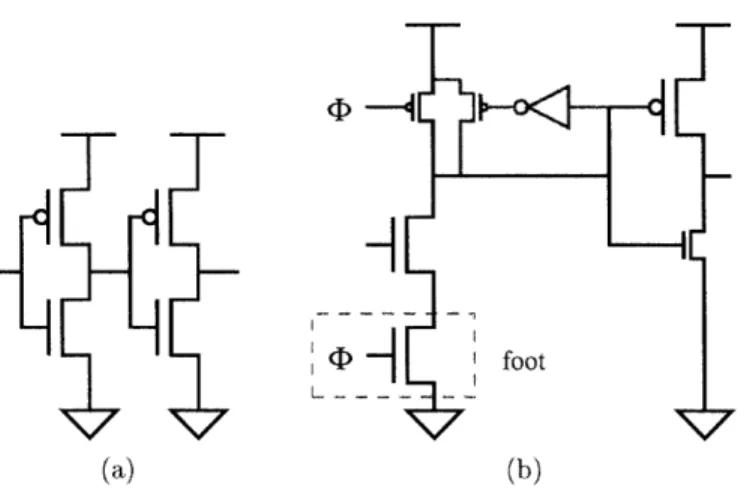
Figure 3-1: Basic logic styles. (a) Static CMOS. (b) Domino. The feedback keeper on the dynamic node, shown in gray, provides noise rejection. Smaller transistors are less critical. The clocked transistor on the NMOS pull-down is not present in the footless variant.
Even better, a pipeline using static gates and Razor latches [15] is also immune to soft error from transient noise (even running at full speed), with little timing overhead and, at the same time, gets speedup from exploiting data-dependent delay variance.
The problem with static CMOS is that it performs too poorly for the most aggressive designs. A full pull-up and pull-down chain are required, meaning that any function requires at least 2 transistors per input. In addition, it is not very efficient in implementing circuits such as XOR/XNOR, wide-fanin NOR, or binary encoded multiplexers, requiring an exponential number of transistors and/or a n transistor pull-up chain for n inputs.
3.2
Domino
A domino logic network [16] is composed of alternating dynamic and static CMOS gates. In a dynamic gate, the PMOS pull-up chain found in a static CMOS gate is replaced with a clocked pull-up transistor, reducing the input load by a factor of 1 + r, where r is the PMOS to NMOS width ratio. When the input clock is low, the dynamic output node is precharged high. When the input clock rises, the gate evaluates, conditionally discharging the dynamic node. If the node does not discharge, the feedback keeper maintains the high value at the dynamic node.
Domino logic is frequently chosen for high-speed design because of the higher perfor-mance of dynamic gates. An indication of the relative perforperfor-mance of static CMOS and dynamic gates can be found in the theory of Logical Effort [17]. Logical Effort is the mea-sure of output drive divided by input capacitance, relative to an inverter. The contribution of a gate to the total delay of an optimal path is shown to be proportional to the logarithm of the logical effort of the gate. The logical effort of common gates are shown in Table 3.1. A dynamic logic gate generally outperforms the equivalent static CMOS logic gate because
the logical effort for each gate is lower.
Table 3.1: Per-input logical effort of common gates, where n is number of inputs. The ratio of NMCS to PMOS drive is assumed to be 2. Static gates are sized to have balanced rise/fall delay.
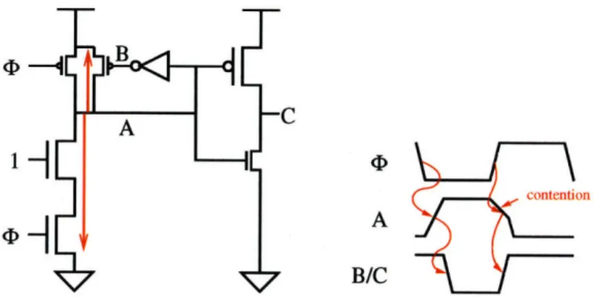
The performance of domino logic comes at the cost of power, robustness, and design effort. Domirno logic burns more power because of the increased number of transitions on the output net. Figure 3-2 shows the operation of the domino buffer when the data input is always high. Note that nodes A, B, and C switch twice on each cycle, though they are conceptually holding constant values. The nodes in a static CMOS buffer would not be switching at all. More generally, for uniformly random input data, the nodes driven by a domino buffer will toggle twice as often as the nodes driven by a static CMOS buffer, neglecting glitching activity. Note also that the feedback inverter and node B would not exist in the static C'MOS version; thus there is extra capacitance being switched. In addition, domino logic presents a much greater clock load than static CMOS, and thus requires greater power to drive. Compared to data nodes of the same capacitance, clock nodes account for more power dissipation because of clock tree buffering and greater switching activity. Further, the feedback keeper also burns power and degrade performance because of contention when the dynamic gate switches. This is shown in Figure 3-2. After precharge, the dynamic node is high, meaning that the feedback keeper is on. When both the data input and the clock go high, the pull-down chain tries to drive the dynamic node low. The pull-down chain has to fight the keeper until the keeper itself changes state. The amount of contention, and hence delay degradation and power waste, depends on the relative sizes
of the transistors in the dynamic gate and the feedback keeper.
Another complication is that some form of latching is required in between the clock stages. This is because the final domino precharge in the stage erases the output right when the domino gates in the next stage begin to evaluate. Without a latch, the NMOS chain will not have enough time to fully pull down. The latch (or half-latch) captures the data before the falling edge of the clock that triggers preset, giving evaluate time to work. Extra clock phases or non-50% duty cycle clock waveforms can also solve this issue, at the cost of some complexity.
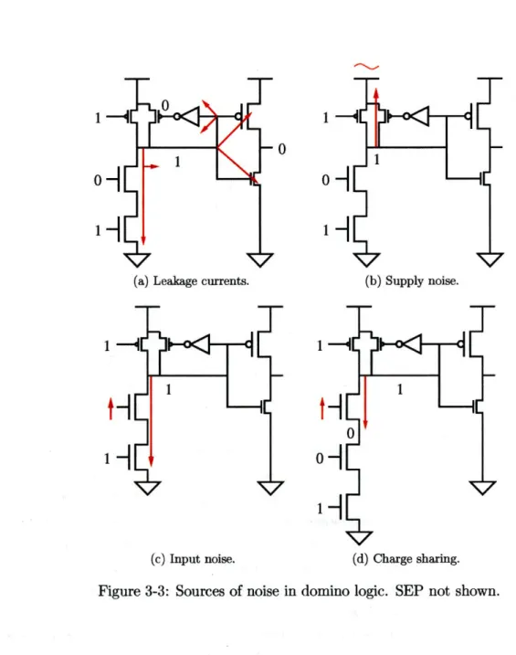
The absence of a static pull-up chain makes a dynamic gate susceptible to input noise, power and ground bounce, leakage, charge-sharing, and SEP during the evaluate phase if
Logical Effort
Gate Type Static Footed dynamic Footless dynamic
INV
1
2/3
1/3
NAND (n + 2)/3 (n + 1)/3 n/3
NOR
(1 + 2n)/3
2/3
1/3
one-hot MUX 2 1 2/3
A B/C
Figure 3-2: Domino switching and contention. Nodes A/B/C always toggle even though the input is held steady. Contention occurs whenever the evaluate stack begins to pull down.
the outputs are not being pulled down (Figure 3-3). Without the feedback keeper in these circuits, the gates would have zero noise rejection and the dynamic nodes will discharge completely given enough time. The feedback keeper placed on the dynamic node maintains the charge on that node, giving the gate some degree of noise-rejection. The noise rejection capability of the circuit depends on the relative sizes of the transistors in the dynamic gate and the feedback keeper. However, note that if the dynamic node incorrectly discharges past a certain point, the result is irreversible and incorrect computation will result; the Razor technique [15] is thus ineffective in improving robustness in domino logic. However, the Razor technique can still be applied to improve performance by exploiting data-dependent delay variance.
In addition, the static gate that follows the dynamic gate in domino logic has a profound influence on the overall noise margin. The static gate tends to be heavily skewed to favor rising transitions, since the falling transition is not a factor in performance. This, however, compounds the heavy skewing in the dynamic gate, resulting in diminished noise margins. In order for domino logic to maintain good noise margin, designers must sacrifice power and performance by increasing the size of the PMOS keeper and the following NMOS chain.
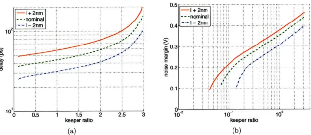
The sizing of the feedback keeper in a domino gate is critical. Figure 3-4a shows the delay vs. keeper ratio (P/N width) of a PTM [18] 32nm 2-input footless NOR gate at 0.6V, 1000 C. We observe a super-exponential dependence of delay on the keeper ratio. Beyond a ratio of about three, the gate fails to evaluate. Figure 3-4b shows the noise margin (DC latrge-signal unity gain input level) vs. keeper ratio. There is an exponential dependence of required keeper ratio vs minimum noise margin. We see, then, that we can have large delay and large noise margin, or small delay and small noise margin. There is always a trade-off. The maximum acceptable delay sets the upper bound on the keeper ratio, while the minimum acceptable noise margin sets the lower bound on the keeper ratio. In fact, the trade-off is extremely sensitive; the delay is super-exponentially dependent on the keeper ratio which is again exponentially dependent on the target noise margin. Further, the
0
1
1
(a) Leakage currents. (b) Supply noise.
1
1
1
t
0
1
(c) Input noise. (d) Charge sharing.
Figure 3-3: Sources of noise in domino logic. SEP not shown.
0
... I
'-I+2nm
I... R ... . . . . .. - nominal iI i : : / ,"mnma n··o ,
SI 2nm 0.4 ... ..... .. ... ... ... i ... ... ... .: .... ,,-:' : '"'!• '/ ... •... ... . ... i .... ... ... .. .. ... ... "• ... •. ... ... .. ! ... : ... ... !. . .. ; " " ...s -... . ., z...
.'
.r...
i , .*
.. ... ... .. . . .... ..-.. .. •.... .... " ... G O .3 $0.2 ... ...: ... ... ... ... . . . ... ... ,. ,• .. ... •• .:,; ..:.... ... .. ... ... -- 1+2 nm. --- nominal : .i ./ .-.- I.-2nm ... .... . .. 9 V· : .. . . .. . .. :. : :..:.::. ::.. ...:.. :... : :.. .... . .:... .... . . . .. .. . .... .. • , : : : :::: ., : : : : : : • . •. . ,.•. .. . . . . .0
0.5
1
1.5
2
2.5
3
102
o-'
o0
keeper ratio keeper ratio
(a)
(b)
Figure 3-4: Keeper sizing for a PTM 32nm 2-input footless dynamic NOR gate at 0.6V,
1000 C. Channel lengths are varied by +2 nm. (a) Delay vs. keeper ratio. One input varying
with 25ps input rise time. Second input constant 0. 740nm evaluation width. 20fF load.
(b) Noise margin vs. keeper ratio. Both inputs varying.
off between performance and noise margin gets worse with scaling. The acceptable range of keeper ratios shrinks as technology scales [19].
To make matters worse, domino logic is sensitive to variation. Figure 3-4 also shows the keeper sizing curves when the transistor channel lengths are varied by +2 nm, corresponding to approximately 3a process deviation [2]. Correct operation requires delay to be verified at the slow corner and noise margin to be verified at the fast corner. This further shrinks the range of acceptable keeper ratios. As relative device variability increases, this effect will become larger.
Footless domino pipelines require separate delayed clocks for each stage of logic, each separated by two slow inverters. The timing constraints for the clocks are complex. The rising edge of each stage's clock should precede the rising edge of data for performance. The falling edge of each stage's clock should follow the falling edge of data to prevent contention. This careful clock shaping is also sensitive to variation. The clock generation requires extra area and power and, because of their complexity, are appropriate only in critical datapaths and in wide-or structures such as register files where the clock delay circuitry can be amortized across many gates in a stage. These schemes also require careful analysis. One must account for process and environment variation to ensure accurate tracking of clock and data delays.
Because of the keeper sizing issue, the delay/robustness trade-off, and variability con-cerns, it is not clear how well dynamic circuits will scale into the nanometer regime. A study of technology scaling on CMOS Logic styles was performed by Anis et al. [20]. They showed that, for the technology nodes from 0.80 pm to 0.25 tim, the performance advantage of domino logic over static logic is reduced. Another analytical study by Anders [19] showed
10'
-i
.".
that if we ho:"d noise margins to a constant fraction of the supply voltage, the performance of dynamic circuits are severely degraded at the 70 nm node, and conventional dynamic circuits cease to function below 70 nm. This last prediction, however, was flawed because it presumed voltage scaling would continue. Nevertheless, domino circuits will continue to face serious noise and scaling issues.
In addition to power-performance-robustness scaling issues, domino logic requires ad-ditional design effort because of complex intra-cell routing and routing to reduce noise. Finally, domino logic can only implement non-inverting logic functions, which limits it use. Variations on domino logic such as dual-rail domino, or use of deracers or complementary signal generators [21], enable inverting logic, but at the cost of increased power and area.
3.3
Conclusion
Static CMOS logic and Domino logic occupy very different points in the energy-delay-robustness space. Static CMOS is good in terms of energy and energy-delay-robustness, but is poor in terms of delay. Domino is good in terms of delay, but is poor in terms of energy and robustness. Ii. particular, it cannot take advantage of the Razor technique for robustness against transient noise. Finally, domino has serious scaling issues. In the following chapters, we show how PSSL combines the best features of static CMOS and domino.
Chapter 4
Preset Skewed Static Logic
In this chapter, we present Preset Skewed Static Logic (PSSL). PSSL combines the energy-efficiency and robustness of static CMOS logic with the performance of domino logic. We first show how Skewed Static Logic can improve performance in the presence of timing slack. We then show how to generate slack through preset. We then show the implementation of PSSL logic and PSSL pipelines. Finally we discuss various scaling issues with respect to PSSL.
4.1
Skewed Static Logic
Figure 4-la shows a chain of four static CMOS inverters. The dashed curve indicates the transistor activation path, that is, the sequence of transistor chains that are turned on, for a rising input transition. The solid curve indicates the transistor activation path for a falling input transition. Note that the total path delay times of a rising input and that of a falling input are not necessarily the same. There is a trade-off between the two delay times and also between delay and energy; this is controlled by varying the sizes of individual transistors. For example, by increasing the size of transistors under the dashed curve, one can speed up the response of the circuit to a rising input transition. This comes at the cost of a slower response to falling input transitions and increased energy dissipation. Figure 4-1b shows this trade-off. The plot shows the energy and delay of two inverters within a long fan-out-of-4 (F04) chain. The X and Y axes represent delays through rising input and falling input paths. The shade at each x,y location indicates the required energy dissipation to achieve the delays. Note that the shade axis is logarithmic.
More generally, consider any multiple-input, multiple-output acyclic combinational cir-cuit. There can be many activation paths. If there is any difference in the delay times between different paths, then there is slack. By appropriately resizing transistors, one can often use slack to either increase performance or reduce power dissipation.
700 600 500 -400 O 300 200 100 S 0 100 200 300 400 500 600 700 delayr (ps) -114 -11.6 -12 -122 F -12A (b)
Figure 4-1: (a) Inverter Chain (b) Energy-Delay. TSMC 0.18/,Im process. F04 configura-tion. 10.4fF wire load.
4)
A C
A B B
C
Figure 4-2: Preset Skewed Static Logic. Smaller transistors are less critical.
4.2
Preset
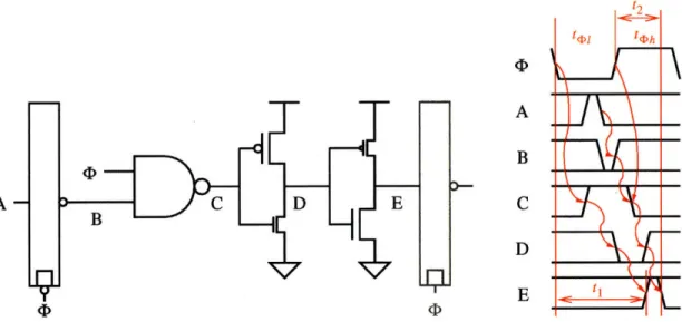
A simple PSSL circuit is shown in Figure 4-2. This resembles the chain of static inverters in Figure 4-la, except that the first inverter has been replaced by a NAND gate with one input tied to the clock. The logical function of this circuit is the same as the inverter chain.
Let us assume that the input A is expected to arrive at the rising edge of the clock. The operation of this circuit as is follows. First, the falling edge of the clock initiates the process of preset. In preset, all circuit nodes are indirectly forced to pre-determined values. In particular, node B rises in turn causing node C to fall, thus completing the preset process. The idea behind the preset process is that we are speculatively computing all the nodes of the circuit presuming low input values. This begins one clock phase before the actual input value(s) arrive, so this computation has an extra clock phase to complete.
The rising edge of the clock initiates the process of evaluate. Note that the process of evaluate is independent of the process of preset, and, in particular, evaluate can begin before preset completes. If the value of the input node, A is low at the rising edge of the
-(b)
A-I
B
A-out
-B
Fi.gure 4-3: A 2-input NOR embedded in PSSL preset-high circuitry.
clock and remains low, nothing further happens in the circuit and evaluate is complete. However, if the input node, A, is high when the clock rises or node A rises while the clock is high, then it causes node B to fall, in turn causing node C to rise, completing the evaluate process.
Whether node A is high or low, eventually node C gets the correct value. However, we have decoupled the computation for low values of A (the preset process) from the computa-tion for high values of A (the evaluate process), giving the former computacomputa-tion extra time and thus creating slack in the path of transistors in the preset process (i.e. the preset path). We can take advantage of this slack by reducing the size of transistors in the preset path to reduce power consumption, or by increasing the size of transistors in the evaluate path to reduce delay. Preset allows PSSL to outperform generic static CMOS logic. However, preset comes at the cost of extra power consumption because of spurious transitions from input mis-speculation and extra clocking overhead.
A NAND ga~te was used to preset nodes high. A similar analysis holds if we use a NOR gate for preset. This time, preset is initiated by the rising edge of the clock, and node B of Figure 4-2 is preset low.
One can embed logic into the gate used for preset. Figure 4-3 is an example of a 2-input NOR gate folded into a preset-high gate. For logic embedding, it is usually preferable to use preset-high since only a single NMOS transistor is added to the NMOS chain of logic gate. For preset-low, a PMOS transistor is added to the PMOS chain of the logic gate. The latter
has a larger energy-delay impact.
4.3
Unateness
Speedup from preset depends upon the decoupling of the computation for high and low inputs. This requires that the preset and evaluate paths go through distinct sets of
transis-Figure 4-4: Non-unate logic. Since the bottom input of the XOR gate cannot be known
a priori, a rising input at the top input produces an unknown transition at the XOR gate
output, producing unknown transitions for all downstream logic.
tors. If the paths coincide at a transistor, the worst case timing path will apply, reducing the benefits of preset. The paths are distinct only if the boolean logic function being imple-mented is unate, meaning that any particular input transition in any particular direction can only cause the output to transition in one direction. In others, it is always inverting or non-inverting. Figure 4-4 shows a non-unate logic network, consisting of an XOR gate and an inverter. Since the bottom input of the XOR gate cannot be known a priori, a rising input at the top input produces an unknown transition at the XOR gate output, producing unknown transitions for all downstream logic.
Even if a function as a whole is not unate, it may be composed of unate subfunctions. These subfunctions can benefit from preset. Performance can be maximized by locating non-unate blocks as far downstream from preset circuitry as possible.
4.4
Pipelining
We now examine how to create pipelines using PSSL. We present PSSL using the three major clocking schemes: level-sensitive, edge-triggered, and pulsed.
4.4.1
Level-sensitive
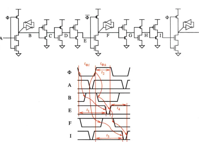
Level-sensitive clocking uses alternating transparent latches as timing elements. A two-phase Level-Sensitive PSSL (LS-PSSL) pipeline, shown in Figure 4-5, is the composition of PSSL pipeline stages of alternating phase, separated by transparent latches. One stage begins preset when adjacent stages begin evaluate. In LS-PSSL, the transparent latches serve two purposes. First, they hold pipeline state. Every legal (non-wave pipelined [22]) pipeline must have at least one latch in each full pipeline stage. Second, the latches prevent the preset wave-front from propagating to the following stage until after the preset phase. Otherwise, if the wave-front propagates early, it will cause inter-symbol interference as it becomes indistinguishable from the evaluate wave-front from the previous cycle. However, in contrast to their use in static CMOS pipelines, transparent latches are not used for
A
B C
D E
Figure 4-5: Two stage Level-Sensitive PSSL pipeline and timing diagram. Only half of the pipeline is shown. Smaller transistors are less critical. 50% duty cycle clocks are assumed.
synchronization (i.e. delay). Every legal pipeline must have a total of exactly one cycle of delay in each full pipeline stage. In LS-PSSL, the synchronization is performed by the NAND gates.
The operation of LS-PSSL, shown in Figure 4-5, is as follows. The falling edge of the clock begins preset, causing C to rise, D to fall, and finally E to rise. This path, whose delay is tl, must complete in one clock cycle, less setup delay. This coincides with the closing of the second latch at the falling edge of the clock. Therefore we derive the constraint
tl + ts < t4h + t41 (4.1)
where t, is the setup time of the latch.
The rising edge of the clock begins evaluate. The value of A is effectively sampled by the first latch and NAND gate combination at the rising edge of the clock. If it is low, then
C falls, D rises, and, finally, E falls. This path, whose delay is t2, must complete one setup
delay before the closing edge of the latch. Therefore we derive the constraint
t2 + ts < t4h (4.2)
Similarly, the equations of the other half of the pipeline (not shown) are given by
t3 + ts < t4el t+ h (4.3)
t4 + ts < t41 (4.4)
The preset path delays, tl and t3 can be twice as long as the evaluate path delays, t2 and
t4.
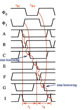
tql t 4 h (D1 A B C time I E F G I time borrowing t2 t4
Figure 4-6: Two stage Level-Sensitive PSSL pipeline timing with overlapping clocks.
Note that there is a hard edge on every constraint. Each timing path begins at a clock edge and ends at a clock edge. This means that clock uncertainty, or jitter, needs to be considered in maximum delay timing analysis. Even worse, for t2 and t4, the jitter needs
to be subtracted from each phase, not just each cycle. However, if we allow the clock waveforms to have greater than 50% duty cycle so that the clocks overlap, then limited time borrowing is allowed as data can flow through the NAND gate before the preceding latch closes[23] (Figure 4-6). Therefore, in this case, jitter does not need to be taken into account for maximum delay analysis. The equations 4.2 and 4.4 are thus replaced by
t2 + t4 < t4h + t41 (4.5)
A problem with using overlapping clocks is that the latches no longer prevent the preset wave-front from advancing early. Therefore, all preset paths must meet a minimum path delay in order to guarantee correct operation, as if the circuit were wave pipelined. These
constraints are given by
tel < t1 (4.6)
tch < t3 (4.7)
We can also resolve this by using K' for the latch clock instead of 4'-1. This allows time borrowing on the evaluate path, but not time borrowing on the preset path.
Latch and preset implementation
Table 4.1 shows eight implementations of the latch and preset gate for level-sensitive PSSL. Row (a) is an implementation of Figure 4-5. Since the latches are used in PSSL mainly to prevent the preset from interfering with the evaluation of data from the previous cycle, the latches can be simplified under certain conditions. These simplified variants are shown in rows (b) through (h).
The variants differ in their properties. This is shown in Table 4.1. The preset/precharge input constraints column indicates the required logic level (on preset) of any input signals that are preset or precharged. The functional constraint column lists which input edges (rising or falling) must arrive prior to the rising edge of the clock, Qn, to guarantee the correct functionality of the circuit. The timing constraint column lists which input edges (rising or falling) must arrive prior to the rising edge of the clock for there to be any benefit from preset. The functionality of the circuit is not otherwise affected by not meeting this constraint. The time borrow column lists which input edge, if any, can benefit from time borrowing. Note, though, that a timing constraint on the same edge precludes time borrowing for all practical purposes. Finally the output preset column indicates the logic level to which the output is preset.
The variants shown in rows (g) and (h) combine the latch and preset gate into one dynamic gate. They are equivalent to the variants in rows (d) and (e), except for output inversion. The dynamic gate variants have lower energy and delay and so are usually preferable. Even though PSSL can use dynamic gates, as domino does, they are used for completely different purposes. In domino, the dynamic gates are used for their high performance. In PSSL, the dynamic gates are used to preset downstream logic. Preset is the source of speedup. Even if the PSSL dynamic gate were slower than its static equivalent, PSSL would cutperform static CMOS.
The simplified versions allow time borrowing because of the partial removal of latching. An example pipeline and timing diagram are shown in Figure 4-7.
If the preset/precharge constraints are violated, the state node is not protected from corruption by preset. However, the circuit can still operate correctly if the preset paths are sufficiently slow as to not interfere with the evaluation of the previous cycle. This is a form of wave pipelining [22]. Formally, this means that one or both of the following minimum path delay constraints must be met.
tl < tl (4.8)
tDh < t3 (4.9)
A reasonable design, however, should ensure that these minimum path delay constraints apply to only one clock phase so that the clock can be stopped on the other clock phase for standby operation.
input constraints preset/precharge functional
time output timing borrow preset
A B
E
F
Figure 4-7: LS-PSSL time borrowing. Full pipeline shown. Smaller transistors are less critical.
One complication arises in connecting the output of 2-phase non-overlapping footed domino logic to the input of LS-PSSL. The domino output can be a narrow pulse around the rising edge of the capturing clock. The dynamic preset gates may not work correctly since they begin sampling after the rising edge. The best solution is to use one of the latch/NAND combinations, with T for the latch clock.
N-phase clocking
It is possible to extend LS-PSSL to arbitrary numbers of clock phases, as in Figure 4-8. As with a 2-phase LS-PSSL pipeline, each preset path is allowed one cycle to complete. The evaluate paths are allowed, on average, 1/n of a clock cycle. This means a factor of n speedup on the preset paths. N-phase LS-PSSL, where n > 2, differs from two-phase in that time borrowing is allowed on the evaluate paths even when the full latch (see Table 4.1a) is used with 50% duty-cycle clocks[23] since the clocks will always overlap. There is also no preset minimum path delay problem as would occur with a 2-phase overlapping clock design since the rising edge of one clock follows the falling edge (from the previous cycle) of the following clock.
The analysis is different when using dynamic gates for the combined latch and preset (see Table 4.1g and h) since there is no separate clock for latching and preset. Figure 4-9
A
D A 4) 1 B 2 C
43
Figure 4-8: 4-phase LS-PSSL. Time borrowing is enabled by the overlapping clocks.
3 (Do 1
A
a-(b) (c)
Figure 4-9: N-phase LS-PSSL using dynamic preset and clock waveforms. (a) Partial pipeline shown. Smaller transistors are less critical. (b) 4-phase 50% duty cycle clock input waveforms. (c) 4-phase 25% duty cycle clock input waveforms. Preset path timing is shown in red.
(D2
4)0
(D¢2
A
B
C
D
EQ
Figure 4-10: Edge Triggered PSSL and timing diagram. Full pipeline shown. Smaller transistors are less critical.
shows the pipeline using dynamic preset, along with two timing diagrams with different clock waveforms. As in the two-phase case, the preset path begins at the falling edge of the clock and ends with the rising edge of the clock to the next stage. Using 4-phase 50% duty cycle clocks, the preset paths can take 3/4 of a clock cycle, for a speedup of 3 on the preset paths. Using 4-phase 25% duty cycle clocks, the preset paths can take one whole clock cycle, for a speedup of 4. In general, n-phase 50% duty cycle clocks achieve 1 + a speedup whereas 1/n duty cycle clocks achieve n speedup.
4.4.2
Edge-triggered
As opposed to level-sensitive clocking, edge-triggered clocking uses a single monolithic
tim-ing element (usually a flip-flop). Figure 4-10 shows a pipeline ustim-ing the same latch and
NAND gate combination as before. However, this time there is only one set in a full pipeline stage, along with the diagram diagram. The corresponding timing constraints are
tl + ts < tPh + 2tel (4.10)
t2 + ts < t + t41 1h (4.11)
tl > tl (4.12)
The timing paths being and end on clock edges so that there is no time borrowing allowed. Note that there is a minimum path delay constraint on clock phase 2. Violating this constraint would cause inter-symbol interference. This is a fundamental race condition that cannot be avoided. It is impossible to have a data valid window greater than a clock cycle. The constraint means that the clock can only be stopped on clock phase 1 (clock high). With a 50% duty cycle clock, a speedup of a factor of 1.5 can be achieved for the
A 7C A B C D E
Figure 4-11: Pulsed PSSL pipeline with timing diagram. Full pipeline shown. Smaller transistors are less critical.
preset path. If the clock is a narrow pulse, a theoretical speedup of a factor of 2 can be achieved. However, finite rise/fall times and the requirements of latching impose a lower limit on the clock pulse width.
4.4.3
Pulsed
Pulsed clocking uses transparent latches that are clocked with narrow pulses. Figure 4-11 shows a pulsed PSSL pipeline along with its timing diagram. It uses a novel flip-flop structure which we call the Double Pulsed Set Conditional-Reset Flip Flop (DPSCRFF) [24]. In the DPSCRFF, the path from input to output is only a single stage of logic. This is the key to the design's high-performance. Another advantage is that the data input sees only a single transistor load which reduces required input drive and energy consumption. The pulse, ir should be timed to follow the rising edge of the clock, Ia. As with the edge-triggered PSSL, there is an unavoidable race condition, the preset path must take longer than a clock phase. The timing constraints in the general case are given by
t&l + td, + tw, < tl (4.13)
tl < toh + 2teI + tdx (4.14) td7 + twr < t2 (4.15)
t2 + ts < tbh + tl + tdr (4.16)
td, + tw7 is the hold time of the pulsed-latch. No time borrowing is allowed in the general case.
If the intervening logic is strictly inverting, then the timing constraints are given by
t4l
+ tda < tl (4.17)tl < tPh + 2tDl + tdr (4.18)
td7r + tw7 < t2 (4.19)
t2 + ts < t< h + t4 +± tdr + tw- (4.20)
Limited time borrowing is allowed in the evaluate path if it completes in the middle of the latching clock pulse.
If the intervening logic is strictly non-inverting, then the timing constraints are given by
t4l + tdfr + twTr < tl (4.21)
tl < toh + 2t1, + tdr- + twn (4.22)
tdw < t2 (4.23)
t
2+
ts < t + tdl Ah + td7 (4.24)Limited time borrowing is allowed in the preset path if it completes in the middle of the latching clock pulse.
In this pipeline, all the state is held in the DPSCRFF outputs. Since these are erased when the clock is low, the clock can only be stopped when the clock is high. Fortunately, there is no minimum path delay constraint on phase 1. One of the potential problems with pulsed clocking is the minimum path delay constraint on phase 2. However, this can usually be resolved without slowing down critical paths.
With a 50% duty cycle clock, a speedup of a factor of roughly 1.5 can be achieved for the preset path. A theoretical speedup of a factor of 2 can be achieved if the pulse is made infinitely small and is moved to the right before the falling edge of the clock. However, finite rise/fall times and the requirements of latching impose a lower limit on the pulse width. In addition, the output of the DPSCRFF becomes a narrow pulse, so there is the concern that the data pulse might actually dissipate before reaching the next stage. Fortunately, the skewing of the logic works to stretch out the pulse. However, the pulse integrity would still need to be verified across process corners.
Pulsed-PSSL and edge-triggered PSSL have similar timing properties. Assuming that clock pulse generation is not a problem, it is clear that pulsed-PSSL is superior to edge-triggered-PSSL because of the lower device count and latency of pulsed-PSSL. Therefore we do not consider edge-triggered PSSL in the evaluations.