A
CMOCS-Comnatihle C omnct
T)Dignlav
... .... "by
Andrew R. Chen
Bachelor of Science in Electrical Science and Engineering
~ , . . ~ . .. r ran ,r t T ~ r AN~ /-1
MAssACHUSS
OF TECh'Nt )OGY
OCT 21 2005
LIBRARIES
Massachusetts Institute ot 'lechnology, June 1990
Master of Engineering in Electrical Engineering and Computer Science
Massachusetts Institute of Technology, June 1997
Submitted to the Department of Electrical Engineering and Computer Science in Partial
Fulfillment of the Requirements for the Degree of
Doctor of Philosophy
at the
MASSACHUSETTS INSTITUTE OF TECHNOLOGY
June, 2005
©
2005 Massachusetts Institute of Technology
All Rights Reserved
Signature of Author ...
, ...
Y.
Department of Electrical Engineering and Computer Science
April 27, 2005
Certified
by ...
...
.. ... , ...
Hae-Seung Lee
Professor of Electrical Engineering
/
[
/if
Thesis Supervisor
Certified by ...
...
...
~~/ ~
Akintunde I. Akinwande
Professor of Electrical Engineering
Thesis Supervisor
Accepted by.(y,-~C.i'
..--.Accepted
by
..... .. .... .L
... -:Arthur C. Smith
Chairman, Committee on Graduate Students
Department of Electrical Engineering and Computer Science
MASSACHUSETTS INST1ITUTE
OF TECHNOLOGY
OCT LIBRARIES2005
A CMOS-Compatible Compact Display
by
Andrew R. Chen
Submitted to the Department of Electrical Engineering and Computer Science
on April 27, 2005, in partial fulfillment of the requirements for the degree of
Doctor of Philosophy in Electrical Engineering and Computer Science
Abstract
Portable information devices demand displays with high resolution and high image
quality that are increasingly compact and energy-efficient. Microdisplays consisting of a
silicon CMOS backplane integrated with light generating or modifying devices, are being
developed for direct-view and projection applications.
A microdisplay architecture using silicon light emitters and image intensification
suit-able for a micro-projector application is developed. A standard low-voltage CMOS IC incorporating display drivers and an array of avalanche diodes produces a faint optical image, and an image intensifier efficiently amplifies the image to useful brightness. This architecture has high efficiency and the potential to achieve adequate luminance for
pro-jection applications. A proof-of-concept system with 16x32 arrays is implemented and
evaluated.
A high-performance silicon backplane for the above system is designed, implemented,
and evaluated. The backplane is a standard CMOS die including a 360x200 pixel array with silicon light emitters, and 10b precision current-mode driver circuits. The driver
cir-cuits can support a number of emissive display technologies including silicon light emitters
and organic light emitting diode (OLED). They employ a self-calibration technique based
on the current copier circuit to minimize variation and fixed-pattern noise while reducing circuit area by a factor of five to seven compared to a conventional solution. A circuit
technique to improve the retention time of dynamic analog memories is also presented.
This technique allows a dynamic analog memory to retain 10b precision for 500ms at room
temperature.
Thesis Supervisor: Hae-Seung Lee
Title: Professor of Electrical Engineering
Thesis Supervisor: Akintunde I. (Tayo) Akinwande
Title: Professor of Electrical Engineering
Acknowledgements
FIRST
I would like to thank my co-advisors Harry Lee and Tayo Akinwande for their
support and thoughtful guidance throughout my doctoral program. They have helped
me with matters large and small, from technical answers to publishing and professional
planning. Their straightforward style and pursuit of quality results are a source of
inspira-tion for many students. I would also like to thank Tom Knight for reading my thesis and
providing insights into the design of microdisplays.
It has been a privilege to be part of the Lee-Sodini lab, and I am thankful to my friends and labmates for the discussions, help, and fun times we have shared. Iliana Fujimori showed great patience and teaching skills not only as a co-teaching assistant, but also by
introducing me to imagers, and sharing test chips with me for making initial measurements.
I've learned a lot from Todd Sepke, Anh Pham, and Albert Jerng with whom I've shared
a cubicle for the last two years. Mark Spaeth provided a much wisdom in printed circuit
board design, and arcade games. Pablo Acosta, Ayman Shabra, Mark Peng, Don Hitko, and Dan McMahill all had answers to my persistent questions as I started my research.
I am thankful to Duane Boning for introducing me to the intricacies of process variation
in semiconductor manufacturing. This basic knowledge is valuable at all levels of circuit and system design.
Thanks to Professor Vladimir Bulovic and Yakov Tischler for help in making optical
measurements, and for advice relating to organic LED technology. John Kmyssis and
Annie Wang provided help with electro-optical measurements and data analysis.
I am grateful for the support of family and friends. My fiancee Lucy has consistently encouraged me and helped me to grow. She has also put up with my graduate student work hours. Thanks to my friends for sharing these years together. Although many of us are scattered around the country, we are still close. My parents have cared for me for all these years, and I will always love them.
Integrated circuit fabrication was provided by National Semiconductor. Peter Holloway,
Matt Courcy, Mike Guidry, Sangamesh Buddhiraju, and the physical design staff all
con-tributed valuable advice and assistance.
This research was funded by the MARCO Focus Center for Circuit & System Solutions
Biography
ANDREW
R. Chen received the Bachelor of Science and Master of Engineering degrees
in electrical engineering from the Massachusetts Institute of Technology, Cambridge,
in 1996 and 1997, respectively. From 1997 to 1999 he was a design engineer at Intel
Corporation, Santa Clara CA, designing circuits for Intel Architecture 32b and 64b
micro-processors. He is currently a Ph.D. candidate at the Massachusetts Institute of Technology
studying analog and mixed-signal integrated circuit design.
His research interests include analog and mixed-signal integrated circuit design,
imag-ing systems, and electronic display systems.
Contents
1 Introduction to Displays
1.1 Overview.
1.2 Electronic Display Applications and Technologies
1.3 Brightness and Efficiency ...
1.4 Microdisplays ...
1.5 Micro-projector ...
2 Background
2.1 Silicon Light Emission ...
2.1.1
Previous Work and Applications .
2.1.2
Avalanche Breakdown ...
2.2 Device Measurements ...
2.2.1
0.
8/tm Technology ...
2.2.2
0.35/im Technology ...
2.2.3
0.18tm Technology.
2.2.4
Measurement Summary ...
2.3 Image Intensification ...
2.4 Circuit Design for Displays ...
2.4.1
MOS Transistors ...
2.4.2
DAC Fundamentals ...
2.4.3
Calibration Techniques ...
3 Micro-projector Design
3.1 Design Overview ...
3.1.1
Background: Two-stage displays .
3.2 Micro-projector Efficacy ...
3.3 Test Chip Implementation ...
3.3.1
IC overview ...
3.3.2
Pixel ...
3.3.3 3.3.4 3.3.53.3.6
3.3.7
3.4 Results
Pixel Arrays ...Top-level IC Design and Packaging
System Design .. . . . .
Image Intensifier and Optics ...
Proof-of-Concept System Performance
17 ... . . . 17 ... . . . 18 ... . . . 20 . . . 22 . . . 23 ... 25
... . 25
. . . . 25... . 26
... . 28
... . 28
... . 30
31....
33
37 37 40 4145
. ... . . . . 45 . ... . . . 46 . ... . . . 47 . ... . . . 50 . ... . . . 51 . ... . . . 51 . ... . . . 52 . ... . . . 53 . ... . . . 54 . . . 55 ... . . . 56 . . . 5 7 9 .. . . . . . . . . . . . . . . . . . . . . . . ....
...
...
...
...
. · . . . .3.4.1
Single Pi
3.4.2
Arrays.
3.4.33.4.4
Power M
Discussic
xel ... 57...
58
easurements ...
59
)n ... ... 60 4 Backplane IC Design 4.1 Pixel Array. 4.2 Row Drivers ...4.3 Column Drivers and Calibration
4.3.1 Overview...
4.3.2
Area Comparison ....
4.3.3
Current Copier ...
4.4 Biasing ...
4.5 RefDAC ... 4.6 ArrayDAC ...4.7 Design for Testability ...
4.8 Top-level IC ...4.9 System Board and Optics . . . .
63
... . . . 63 ... . . . 67 ... . . . 68 ... . . . 68 ... . . . 69 ... . . . 70 ... . . . 75 ... . . . 79 ... . . . 83 ... . . . 86 ... . . . 88 ... . . . 895 Measured results
5.1 Electrical Measurements
5.1.1 RefDAC Linearity5.1.2
ArrayDAC ....
5.1.3 Column Variation . 5.2 Optical Measurements ..5.3 Power Measurements . . .
5.4 Sample Images ...
6 Discussion
6.1 Summary 6.2 Topics for Future Investigation A Precision Oscilloscope Measurements 95 ... . . . 95 ... . . . 95...
101
...
103
...
105
...
108
...
108
111 . . . .. 111... ... 112
115...
...
...
...
...
...
...
...
...
...
. . . . . . . . . . . . . . . . . . . . . . . . . . . . . . . . . . . . . . . . . . . . . . . . . . . . . . . .List of Figures
1.1 Applications of electronic displays ...
.
19
1.2 Flat-panel display technologies . . . ... 20
1.3 Micro-projector concept (Fraunhofer-Gesellschaft) . . . .... 24
2.1 Avalanche breakdown I-V characteristic . . . ... 27
2.2 Cross-section of twin-well CMOS process
.
...
27
2.3 Diode I-V characteristic, 0.8/m process . ... 29
2.4 PMOS test device ...
29
2.5 I-V curve for p+/nwell junction in 0.35/um CMOS technology ...
30
2.6 I-V curve for n+/psub junction in 0.35tim CMOS technology . . . ...
30
2.7 Light emission from six parallel test devices . . . ... 31
2.8 I-V curves for two p+/nwell junctions in 0.18um CMOS technology . . . .
32
2.9 Spectra of light emission from junctions on CMOS die . . . 32
2.10 Light output vs. current for junction in 0.18,um CMOS process ...
.
32
2.11 Simple image intensifier application . . . 34
2.12 Microchannel plate (Proxitronic) ... 34
2.13 Intensifier gain vs. number of MCPs . . . 35
2.14 Intensifier resolution vs. number of MCPs . . . ... 35
2.15 GaAs Photocathode Sensitivity (Hamamatsu) . ... 36
2.16 Gate current for an NMOS device .
...
38
2.17 Sample and Hold Circuit models. Left: ideal, Right: realistic ... 39
2.18 Current mirror measurements . . . ... 40
3.1 CMOS IC and image intensifier . . . .. .. 45
3.2 Two-stage display architecture for projection application (JVC) ...
46
3.3 Circuit schematic of a single pixel . ... 52
3.4 Block diagram of pixel array . . . ... 53
3.5 IC photomicrograph ... 54
3.6 Proof-of-concept system board
..
...
54
3.7 Proof-of-concept system with intensifier
.
...
56
3.8 Pixel I-V characteristic, VHI sweep ... 58
3.9 Test image of IC under microscope . . . 58
3.10 32-level grayscale gradient. Bottom two rows are at full intensity ... 59
3.11 Output window of intensifier (20mm) with sample image . . . ...
60
Overview of CMOS backplane ...
Array floorplan ...
Pixel schematic ...
OLED material layers ...
OLED pixel schematic ...
Row driver circuit . . . .. . .
Rnw a.e,'., drive.r timing.a · ~ 'v s .A e, . . . . . . . . . . . . . . . .
Two-stage calibration technique ...
Column driver calibration overview ..
. . .
Simple MOS current source ...
Simple current copier ...
Reduced transconductance current copier . . .
Improved current copier .. . . . .. . . .
Passgate leakage scenarios: (a) conventional, (b) Conventional (left) and improved (right) passgate RefDAC reference current generator and switch
Bleeder bias voltage generator.
VBIAS circuit ...
Testability control circuit ...
Testability scan chain ...
RefDAC block diagram ...
RefDAC current copier circuit .. . . . . .
RefDAC row driver ...
RefDAC column driver ...
RefDAC cell pattern ...
RefDAC copier cell settling time simulation
Retention time improvement circuit . . .
ArrayDAC copier schematic ...
ArrayDAC block diagram ...
ArrayDAC registers ... ArrayDAC data load control.
ArrayDAC calibration control ...
ArrayDAC calibration control, improved . .
Micrograph showing Si-LED pixels, OLED
Column transimpedance amplifier ...
Die micrograph ...
High-level program flowchart ...
Clock oscillator ...
Timing diagram - simple program ...
Timing diagram - optimized ...
Assembled system board ...
. pixel . . ... . . . 64 ... . . . 64 ... . . . 65 ... . . . 66 ... . . . 66 ... . . . 67 ... . . . 67 ... . . . 68 ... . . . 69 ... . . . 70 ... . . . 71 ... . . . 72 ... . . . 73 voltage control . . . . .. 74
:s ...
74
... . . . 76 ... . . . 77 ... . . . 78 ... . . . 78 ... . . . 78 ... . . . 79 ... . . . 80 ... . . . 80 ... . . . 80 ... . . . 81 ... . . . 82 ... . . . 82 ... . . . 83 ... . . . 84 ... . . . 85 ... . . . 85 ... . . . 85 ... . . . 86s, and ArrayDACs . . . . 87
... . . . 88 ... . . . 89 ... . . . 92 ... . . . 93 ... . . . 93 ... . . . 94 ... . . . 945.1 Synchronization circuit ...
5.2 RefDAC bit currents, first attempt ... 5.3 RefDAC bit currents, second attempt ...
4.1 4.2 4.3
4.4
4.54.6
4.7 4.8 4.94.10
4.114.12
4.13 4.14 4.15 4.16 4.17 4.184.19
4.20
4.214.22
4.23
4.24
4.25
4.26
4.27
4.28
4.29
4.30
4.314.32
4.33
4.34
4.35
4.36
4.37
4.38
4.39
4.40
4.41 95 96 97LIST OF FIGURES
RefDAC INL, second attempt ...
RefDAC bit currents, final ...
RefDAC INL, final ...
RefDAC retention test ...
RefDAC retention test, zoomed in . . . .
Transimpedance amplifier circuit . . . .
ArrayDAC INL ...
ArrayDAC retention test ...
ArrayDAC output current distribution ...
ArrayDAC outputs before and after calibration .
Sample image for pixel luminance analysis . .
Pixel luminance variation by column ...
Column luminance ...
5.17 Silicon backplane IC emitting light, showing a se 5.18 Proof-of-concept system with calibrated backplai
... . . . 98 ... . . . 98 . . . 99
...
100
...
100
...
101
...
102
... ... 103
...
104
...
104
...
105
... ... 106
... ... 107
,ries of ramps ...
109
ne ...
109
5.19 Proof-of-concept system with calibrated backplane and alternative optics .
6.1 RefDAC, ArrayDAC, and pixel arrangement.
6.2 Alternative RefDAC, ArrayDAC, and pixel arrangement . . . .
A. 1 Step responses of four oscilloscope probes.
A.2 Probe settling behavior ...
A.3 Four oscilloscope channels, same input ...
A.4 Longer observation time . . . .
A.5 Newer oscilloscope step response . . . .
5.4 5.5 5.6 5.7 5.8 5.9 5.10 5.11 5.12 5.13 5.14 5.15 5.16
.110
.112
.113
.116
.116
.117
.117
.118
13List of Tables
1.1 Typical illumination levels . . . .
1.2 Projector illuminance by application .
1.3 Efficiency of light sources ...
3.1
3.2
3.3 4.14.2
4.34.4
4.5
Intensifier Performance with two MCPs
0.18/um CMOS technology
...
Microcontroller interface definition . . .
PreRef switch truth table ...
ArrayDAC current mirror biasing .
IC power supplies ...
Input pins ...
Output pins . . . . 15. 20
. 21. 22
49
50
5576
8490
9192
. . . . ....
...
...
...
...
...
...
...
Chapter 1
Introduction to Displays
1.1 Overview
This thesis presents work in electronic display design and integrated circuit design.
Elec-tronic systems are becoming increasingly ubiquitous, and displays for a wide spectrum of
applications are being developed. An area of special interest is that of personal portable
electronics, where all system components must be designed for high levels of integration,
compact size, and high energy efficiency. The design of a "micro-projector" for portable
electronic systems is presented. The micro-projector produces an image with adequate
luminance for projection with high efficiency for battery-powered systems.
We propose a micro-projector based on a combination of silicon light emission and
image intensification. A standard low-voltage CMOS IC incorporating display drivers and
an array of avalanche diodes produces a faint optical image. The image is coupled into an
image intensifier that amplifies the image to useful luminance levels. This architecture has
high efficiency and the potential to produce adequate luminance for projection applications.
The advantages of this architecture are compatibility with mainstream CMOS processes,
high efficiency, and potential for projection. Junction diodes which are available in all
stan-dard CMOS processes are used to emit light. Process modifications which are often used
in imagers [26] and microdisplay ICs are not necessary. These junctions can be integrated
with high-performance circuits such as calibrated display drivers. The integrated display
can also be integrated with other circuit blocks to achieve a high level of system integration on a single IC.
The image intensifier is a vacuum device capable of high gain. It uses the mechanism of cathodoluminescence to efficiently generate light, and can produce adequate luminance
for projection applications by using the same principles as projection CRT tubes.
A high-performance silicon backplane for the above system is designed and evaluated.
The backplane is an IC produced in a standard CMOS technology. It includes a 360x200 pixel array with silicon light emitters and 10b precision current-mode driver circuits. The
driver circuits can support a number of emissive display technologies including silicon light
emitters and organic light emitting diode (OLED). They employ a self-calibration technique to minimize variation and fixed-pattern noise while reducing circuit area by a factor of five to seven compared to a conventional solution. A circuit technique to improve the retention time of dynamic analog memories is also presented.
The organization of this document is as follows. The remainder of this chapter is an
overview of electronic display technologies and applications. Chapter 2 provides
back-ground on silicon light emission, operation of the image intensifier, and circuit design concepts relating to display drivers. Chapter 3 presents the design, implementation, and
results of a proof-of-concept display system using two-stage image generation. Chapter 4
presents the design of a high-performance CMOS backplane for the previously described
microdisplay architecture. Chapter 5 describes characterization and measurements of the
system with calibrated backplane. Finally, chapter 6 summarizes and suggests topics for future investigation.
1.2 Electronic Display Applications and Technologies
An electronic display is a device that converts time-sequential electrical signals into spa-tially and temporally configured light signals (images) useful to the viewer [1]. Electronic displays are used in a broad variety of applications, some of which are shown in Figure 1.1.
The variety of applications results in a large number of technologies currently in use
[2, 3]. The cathode-ray tube (CRT) has been a workhorse for many years. Newer displays are based on flat-panel technologies which have the advantages of smaller form factor, lighter weight, and the ability to achieve larger sizes than CRTs.
Flat panel display technologies can be divided into categories as shown in Figure 1.2.
Displays that generate light in response to electrical signals are called emissive displays,
and ones that modulate light are called light valve displays. Examples of mechanisms
used in emissive displays are electron-hole recombination in semiconductors, ultraviolet
radiation exciting a phosphor, or an electron beam exciting a phosphor. Light valves are examples of a broader class of devices known as spatial light modulators (SLM). These create spatial modulation on a plane wave of light by various means, for example by reflec-tion or change in polarizareflec-tion. SLMs require an external source of light which may be a lamp or ambient illumination. The most widely used SLM is the liquid-crystal display. It is versatile and inexpensive, but transmission is typically low and the operation at extreme
1.2. ELECTRONIC DISPLAY APPLICATIONS AND TECHNOLOGIES
Pixels 10M IM lOOK 10K 1K0.3" lin 3in 10in 30in l00in diagonal
Figure 1.1: Applications of electronic displays
temperatures is difficult.
Emissive displays potentially have higher efficiency than SLMs because they gener-ate light only when and were it is needed. In contrast, SLM's require a light source to
constantly produce the maximum display luminance, and dissipate unwanted light as heat.
Emissive and transmissive displays work well under moderate illumination, but have
dif-ficulty producing very high luminance for applications in sunlight. Reflective SLMs work well under high illuminance but have reduced energy efficiency under low and moderate illumination levels where they require an external light source.
Projection systems have the advantage of producing a larger image than than the
sys-tem form factor. Two applications of projectors are digital cinema and portable information
systems. Digital cinema is an application where very large video-rate images are desirable. Flat-panel displays are available in sizes up to 40 inches, but a projector is lighter,
poten-tially cheaper, and easier to scale to larger sizes. Portable electronic information systems
that are becoming smaller and handling increasing quantities of still and video images.
In this application the goal is to produce page-sized images for personal viewing while
keeping a pocket-sized form factor.
The focus of this work is a micro-projector intended personal information systems.
These are compact electronic systems that will include communication, computing,
multi-media manipulation, and data storage. They have been described in literature with various 19
Flat panel displays
Emissive
Modulator
semiconductor: OLED
UV+phosphor: Plasma
electron beam + phosphor:
Cathodoluminescence
polarization: Liquid crystal reflection: micromirror transmission: electrowetting
Figure 1.2: Flat-panel display technologies
Conditions
Illuminance, lux
Direct sunlight
100,000
Open shade 10,000 Overcast day 1,000 Twilight 1 to 10
Full moon 0.1
Indoors, exacting visual tasks 15,000 Indoors, fine assembly work 1,000 Indoors, office 500 Indoors, home 100-200
Table 1.1: Typical illumination levels
terms, such as "information bank system" [4]. The constraints of these systems are
com-pact size, high energy efficiency to maximize battery life, high resolution, high bit depth,
and video speed.
1.3 Brightness and Efficiency
This section describes typical illumination levels of various environments, and the required luminance or illuminance levels for displays. Typical levels of illumination are listed in Table 1.1. The ratio of illumination varies over a 1000:1 ratio from full sunlight to
in-doors at night. This results in a variety of displays optimized for different ambient lighting
conditions.
1.3. BRIGHTNESS AND EFFICIENCY
Table 1.2: Projector illuminance by application
monitor is 25-100 footlamberts. Emissive microdisplays used in head-mounted display
sys-tems (HMDs) require much higher luminances because optical transmission (throughput)
is around 15%. Typical luminance is 1000fL at the display output, which appears as 150fL to the eye.
The required luminance of a projector depends on a number of factors. The contrast
ra-tio determines the rara-tio between maximum projector illuminance and ambient illuminance.
The output of the projector is spread over the image area, leading to a tradeoff between illuminance and image size. The properties of the surface where the image is projected also affect illuminance. An ordinary white surface has a gain of unity. Projection screens with non-uniform reflection patterns can increase gain in a preferred direction, at the cost
of limited viewing angle and contrast. The illuminance of a projector is:
luminance(lumens)
ae(m
2*
gain = illuminance(lux)
(1.1)
area(m2)
where the luminous output of the projector is in lumens, the area of the projected image is in square meters, the gain is unitless, and illuminance is in lux. Required illuminance by application is shown in Table 1.2.
A variety of light-emitting technologies are used today. Table 1.3 compares some
com-monly used ones. Metal halide bulbs are attractive for projectors because of their high
efficiency, high luminous output, and near point-source emission. Organic and inorganic
LEDs are making rapid progress in efficiency, brightness, and the variety of output spectra
available. Phosphor-based light emitters include fluorescent lamps and cathodoluminescent
devices. In these devices, a phosphor converts energy from ultraviolet light or an electron
flux into visible light. Fluorescent lamps are efficient, but because of their large sizes they
can only be used as backlights for modulator-based displays which have low efficiency due
to transmission losses. The cathode ray tube is an example of a cathodoluminescent
dis-play. These can produce extremely high luminance levels, as illustrated by liquid-cooled
tubes used in projection televisions.
Application
Illuminance (lux) Comments
Movie theater
50-80
full control of ambient light
Office 120-150
Ballroom (dimmed)
150-200
Training room (dimmed)
200
Training room (full light)
400
high background illumination
Table 1.3: Efficiency of light sources
1.4 Microdisplays
Microdisplays produce high-resolution images typically less than one inch on a side. They
are commonly used in both the smallest and the largest display applications. Typical near-to-eye devices are head-mounted displays [6] and video camera viewfinders. In these de-vices, optics provide magnification for comfortable viewing. Projection applications in-clude high-definition televisions and computer projectors. In these systems, the microdis-play modulates very high luminance levels from an external light source. Microdismicrodis-play technologies are also being applied to novel applications such as three-dimensional dis-plays [7], switching of optical communication signals [8], high-end photo printers [9], and optical tweezers [10].
An emerging opportunity for microdisplays is the micro-projector. The micro-projector
is part of a pocket-sized personal information device. It projects a high-resolution image
approximately the size of a piece of paper (8in = 20cm) for personal viewing. Its main advantage is the ability to produce images of reasonable size with a very small form factor.
The micro-projector must produce high luminance, high resolution images while being
compact and highly energy efficient. Emissive microdisplays can be designed to have these
characteristics.
Presently the leading technologies for microdisplays are liquid crystal on silicon (LCOS) [11], micromirrors, and organic LED. These technologies can be constructed on top of a
silicon integrated circuit with additional processing. Using a silicon backplane provides
access to high-performance circuits at the pixel or array level, and alleviates the problem of large numbers of interconnect wires between the pixel array and driver circuits.
Liquid crystal displays use an organic material to modify the polarization of light. Pix-els are modelled as capacitive elements and driven with AC voltage waveforms. A variety of circuit techniques for driver circuits have been investigated [12, 13]. Color is usually
Technology
Efficiency (lumens/watt) Notes
Metal halide (HID) 50-100 10-400W
T8 Fluorescent
80
4-foot, 32W
Compact fluorescent
30-60
Cathodoluminescence 48 [5]
OLED 10-30+
White inorganic LED
32+
Halogen 12-20 10-100W
1.5. MICRO-PROJECTOR
achieved by using patterned color filters and sub-pixels for red, green, and blue, at each pixel location.
Micromirrors are an array of mirrors on top of a silicon chip that are controlled electri-cally. At each pixel location, a mirror reflects light to either the output or a heat sink [14]. Color output is achieved in frame-sequential mode using a rotating color filter wheel.
Organic LED is an emissive technology that promises high image quality and
reason-able manufacturing cost. OLED microdisplays with silicon backplanes have been
demon-strated [15, 16]. They promise excellent image quality and potential power savings because
of their emissive nature. OLED performance has been steadily improving, and packaging
and sealing [17] have also improved in recent years. Color can be produced either by
filter-ing of a white image (similar to the case of liquid crystal), or by stackfilter-ing layers of different
light-emitting materials to produce different colors.
1.5 Micro-projector
A micro-projector would allow a pocket-sized electronic system to display high
informa-tion content images and video at a reasonable size for comfortable viewing. Because a projector produces images larger than its own form factor, the system can be pocket-sized
while producing page-sized images. The cost of computation has decreased to a point
where the display, user interface, and battery are primary bottlenecks in portable system
design. A compact display capable of presenting high resolution images and video enables
new uses for portable electronic systems. Figure 1.3 is an illustration of this concept [18].
This contrasts with the flat-panel display approach where the system must be larger than
the image size, or the display must be designed to fold or roll-up when not in use.
Compact projector systems have been demonstrated and are described in the literature.
Keuper [19] describes a projector consisting of a white LED light source, liquid-crystal
modulator, and lens. Projectors using lasers, either a raster-scanned single beam or multiple
beams in parallel, have also been demonstrated [20, 21, 22]. For near-to-eye applications, a laser beam can be modulated and swept onto the retina to produce an image [23, 24, 25].
Laser-based projectors do not require refractive optics for focusing, which may permit
them to be more compact than ones using lenses. They also have good energy efficiency.
The disadvantages of these systems are (1) they require precision mechanical systems to
position the laser beam, (2) they must address the problem of image flicker because they
operate at low duty cycles, and (3) safety concerns if the beam is pointed at the eye, or if
higher power is used to produce high luminance images.
Chapter 2
Background
This chapter presents previous work and preliminary studies on components of our
micro-projector design: silicon light emitters, image intensifiers, and calibrated driver circuits.
An introduction to light emission from silicon is presented along with measurements of
light emitters in standard CMOS processes. The image intensifier and its basic concepts
are introduced.
Display driver circuits are digital-to-analog converters (DACs). An overview of DACs
is presented along with circuit and device considerations that influence their design. A
major concern in data converter design is the management of variation that arises from the
manufacturing process. A circuit called the current copier can produce precise currents
while occupying less area than a conventional solution. The current copier is introduced here, and its implementation is discussed in depth in Chapter 4.
2.1 Silicon Light Emission
2.1.1 Previous Work and Applications
The emission of light from silicon p-n junctions was first reported in 1955 [27, 28]. Since then, it has been used for a variety of purposes. Silicon light emitters were used in a data
storage system to produce dots on photographic film [29]. Light emission from the channels
of MOSFET transistors has been used for debugging and fault analysis of microprocessors
[30]. The idea of using integrating light emitters and detectors on the same chip dates back
to at least 1965 [31], and the application of on-chip optical interconnect is receiving
atten-tion as metal wires have become a bottleneck in the design of high performance integrated
circuits [32].
Silicon is an indirect bandgap material, therefore when electrons and holes recombine
the probability of a photon being emitted is small. This is in contrast to the III-V materials
used commercially in LEDs that are efficient photon sources.
In forward bias, p-n junctions emit photons with energy equal to the bandgap energy. In silicon this is 1.12eV, corresponding to photons with a wavelength of 1100nm. In avalanche breakdown, hot electrons can cause photons with higher energies to be emitted. Light-emitting devices in standard CMOS technologies have been studied [33, 34], and the best reported quantum efficiency is 5 * 10 - 7 phot/elec [35].
Efficiently generating light from a silicon substrate is an area of research interest [36, 37]. Efficiency can be improved by various dopants or altering the shape or material prop-erties of silicon devices [38, 39]. These advances may eventually be integrated into main-stream manufacturing processes. Another solution is the integration of efficient optoelec-tronic devices on a standard silicon substrate [40]. Novel device and circuit designs for light emitters are being explored, for example a structure to lower the breakdown voltage
of silicon light emitters [41].
2.1.2 Avalanche Breakdown
This section explores the properties of silicon junctions in avalanche breakdown used as
light emitters. Light emission from avalanche breakdown produces photons with larger
energies than the bandgap energy. Emission can be in the visible or near-infrared regions of the spectrum.
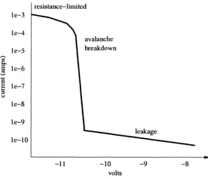
When a junction diode is biased with a large negative voltage, the electric field across the junction is very large. When a conduction band electron enters the field, or is created by thermal processes, collisions with valence electrons can move them into the conduction band. A cascading or multiplying effect occurs, and the current grows dramatically over a small voltage range. The I-V characteristic of a silicon p+/nwell junction in avalanche breakdown has the shape shown in Figure 2.1. Current through the junction grows until lim-ited by external components such as series resistance or a current source circuit. Operating a junction diode in reverse breakdown is nondestructive if the current through the junction is limited. Spinelli and Lacaita [43] provide a more detailed description of avalanche diode physics.
This abrupt characteristic allows the use of low-voltage control circuits. A large DC bias is needed to make the junction enter avalanche breakdown, but once avalanche break-down occurs the change in voltage required to modulate the current is very small. Consider a junction with the characteristic in Figure 2.1. The cathode is connected to a +12 volt sup-ply, and the anode to a "leakage "current sink of lnA in parallel with an adjustable current
2.1. SILICON LIGHT EMISSION
nitedavalanche
breakdown le-3 le-4 le-5 ~le-6 • le-7 le-8 le-9 le-10 -11 -10 -9 -8 voltsFigure 2.1: Avalanche breakdown I-V characteristic
NMOS PMOS
~
~
~
~///////////l/~n///~//1.a~dri
~/////////N/////r/////N/// '/////I//NN//N///~////, ~ ~~Figure
2.2:
Cross-section of twin-well CMOS process
sink. The voltage at the cathode will be 12-10.5=1.5V for currents up to 100PA, producing
a 10
5dynamic range which is more than adequate for display applications.
In a twin-well CMOS process, as shown in Figure 2.2, the p+/nwell junction is the best
suited for integration. It is electrically isolated from other devices on chip. When the
n-well is connected to a high voltage and the p+ region connected to a low voltage, avalanche
breakdown occurs. No substrate currents are created by this structure, and the n-well
volt-age can be safely controlled by MOS devices. The p+/nwell junction breakdown voltvolt-age
is designed to be much higher than the nominal power supply voltage, to ensure proper
operation of CMOS circuits. This reduces the energy efficiency of light emitting junctions,
which should be designed for avalanche breakdown at the smallest possible voltage.
The p+/nwell junction is available in all standard CMOS processes, and low-voltage
devices can be used to drive them. This eliminates the need for more costly high-voltage
processes. In addition, other circuit functions that require high-performance devices such
as processors or memory can be integrated together with light emitters.
In unmodified CMOS processes, avalanche breakdown occurs first around the perimeter of the junction area. This is due to a combination of surface states and the high electric
fields at the edges of the junction area. For a microdisplay using front-emission from a
silicon IC, lateral breakdown is desirable over vertical breakdown because it occurs closer to the surface and allows more photons to escape. Lightly doped guard rings can be used
to modify the doping profile of avalanche diodes if bottom-surface breakdown is preferred,
for example for back-emission from a thin substrate [44].
Avalanche diodes are more commonly used as in sensitive imaging devices for photon counting and operation at low light levels, and many articles have been published on their design in that context [42]. An important design consideration is to avoid covering
light-emitting junctions with silicide. Most CMOS processes include a mask to selectively block
deposition of silicide, and it should be utilized for light-emitting junction areas. Silicides
are deposited over diffusion regions to reduce their sheet resistance. They are nearly opaque
to light and reduce optical transmission by 80-90% [45].
2.2
Device Measurements
A preliminary study was performed to characterize the light-emitting properties and
reverse-breakdown characteristics of p-n junctions manufactured in commercial CMOS processes.
Limited information and data on the use of these junctions as light emitters is available,
therefore we characterized devices manufactured in commercial 0.8um , 0.35um , and
0. 18pm CMOS processes. In all three processes, the p+/nwell junction showed avalanche breakdown behavior when a large reverse bias was applied.
2.2.1
0.8pum Technology
A test device in the Hewlett Packard 0.8[tm (CMOS26G) process is measured. The process
has n-wells, one poly layer, and three metal layers. Nominal operating voltage is 5V. The
test device is the junction between the a source/drain diffusion of a PMOS transistor and
its n-well. Junction area is 50 x 1.5um , and the device is covered with silicide. The electrical characteristics of this device in reverse bias are shown in Figure 2.3. Reverse leakage current rises gradually between 0 and -18V. At -18V, avalanche breakdown occurs and current increases by over six orders of magnitude over a very small voltage range until
2.2. DEVICE MEASUREMENTS
Id vs Vd N76VAF
-20 -15 -10 -5 0
Diode voltage (V)
Figure
2.3:
Diode I-V characteristic,
0.8upm process
Figure 2.4: PMOS test device
it is limited by series resistance.
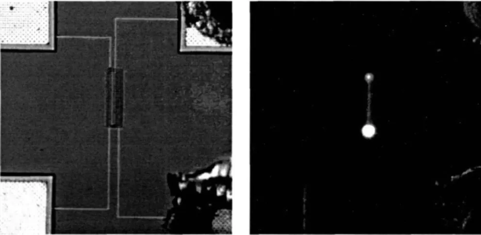
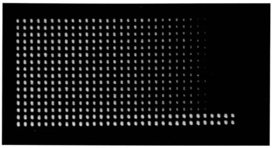
The pictures in Figure 2.4 were created with a CCD camera mounted on a
micro-scope. On the left, the microscope light is on and the four-terminal test device is visible.
The device is connected to four metal pads for use with a probe station. The n-well and
source/drain pads were bonded to package pins for easier testing, and solder from the
bond-ing process is visible on the two pads on the right side. On the right, the microscope light
and room illumination were turned off and a long-exposure image shows light emission
from the p-n junction. Current through the junction is 130PA, and light emission is
con-centrated at the sides and corners of the p+ diffusion area. Light emission was visible in
a darkened room, in agreement with published reports of broadband emission from silicon
junctions in avalanche breakdown.
Chip l1 -d2626 Rverse 03111102 achen 1.OE-02 - - ---1.0E-03 1.0E-04 i 1.0E-05 .0E6- . , oE X 1.0E-07 1.OE-08 1.OE-09 -1.OE-10 -11 -10 -9 -8 -7 -6 Vd (volts)
Figure 2.5: I-V curve for p+/nwell junction in 0.35p1m CMOS technology
Chip #1 d2726 03/11/02 achen 0.01 0.0075 -0.005 0.0025 o 0 -1.5 -0.5 0 0.5 - -0.0025 -0.005 -0.0075 -0.01 ... Vd (volts)
Figure 2.6: I-V curve for n+/psub junction in
0.
35p1m CMOS technology
2.2.2 0.35pm Technology
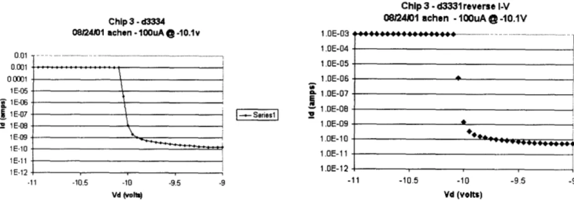
The characteristics of the p+/nwell junction in the TSMC 0.35/um CMOS technology were
measured. The process has n-wells, one poly layer, four metal layers, and silicide block. Nominal operating voltage is 3.3V. Avalanche breakdown of the p+/nwell junction occurs
at -10.OV as shown in Figure 2.5.
An n+/psub junction in this process was also measured, as shown in Figure 2.6. Reverse breakdown occurs due to tunnelling instead of avalanche breakdown, and the I-V character-istic is much less abrupt. Compared to avalanche breakdown, a much larger voltage swing is needed to produce the same change in current. This makes control with low-voltage
devices difficult or impossible. The mechanism of zener tunnelling is not expected to emit
photons, therefore this junction is not useful for light emission purposes.
2.2.
DEVICE MEASUREMENTS
Figure 2.7: Light emission from six parallel test devices
2.2.3
0.18pm Technology
Devices in the TSMC 0.18prm CMOS technology were measured. This process has
n-wells, thin and thick oxide transistors, one poly layer, six metal layers, and silicide block.
Nominal operating voltages are 1.8V for thin oxide devices, and 3.3V for thick oxide
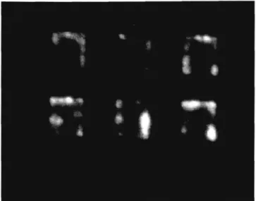
de-vices. The test structure consists of six 12x14[pm junctions connected in parallel, as shown
in Figure 2.7. When this image was taken, ID
=
700pLA and VD = -10.OV.
Reverse
breakdown current-voltage characteristics are shown in Figure 2.8.
Emission occurs at discrete points mostly around the junction perimeter, and luminance
varies between the junction areas due to random manufacturing variation. This variation is
exacerbated by the parallel connection of pixels which allow unevenly located "hotspots"
to carry most of the total current. To improve uniformity, pixels should be small in size
and driven individually by current sources. This technique allows well-controlled
transis-tor electrical characteristics to control light emission instead of poorly controlled junction
characteristics.
The emission spectrum for a p+/nwell junction on the 0.18p/m CMOS chip is shown
in Figure 2.9. In forward bias, the junction emitted photons at its bandgap energy (1.1eV
= 1100nm). In reverse bias, a broadband emission spanning the visible and near-infrared
wavelengths was observed. This is consistent with published data.
By comparing images of the display with a reference target, we estimated the quantum
efficiency of silicon light emitters to be
- 10- 7photon/electron. This value are comparable
to published results for light emission from silicon devices. The silicide layer was not
blocked, so the efficiency of the p-n junction without silicide should be higher.
Chip 3 - d3334
08124101 achen -100uA @ -10.1v 1.OE-03
1.0E-04 1.0E-05 1.0OE-06 I 1.OE-07 __ _Seris_ | - 1.OE-08 1.0E-09 1.OE-10 1.OE-11 1.0E-12 -11 -10.5 -10 -9.5 Vd (volts)
Chip 3 - d3331 reverse I-V 0824101 achen -100uA a -10.1V 4 A .t..._ _' ..
-11 -10.5 -10 -9.5 -9 Vd (volts)
Figure 2.8: I-V curves for two p+/nwell junctions in 0.18pm CMOS technology
35 30 25 20 15 10 5 Chip #3 d3334 forward 20s - 08.27.01- achen .0 10 10 0 Chip #3 d3334 reverse 20s -08.27.01 -Series1 800 850 900 950 1000 1050 1100 1150 1200 wavelength (nm)
Forward bias
600 500 400 300 200 100 04 45-, r-- 4,
- f:'"
0 550 650 750 850 950 wavelength (nm) Reverse biasFigure 2.9: Spectra of light emission from junctions on CMOS die
PMT Vout vs. d - Chip 3 logilog 10102102 achen, Johnkym 10000 1000 0 100 10 01 10 100 -Id (mA)
Figure 2.10: Light output vs. current for junction in 0.18,um CMOS process
o ! .u -Snes1| j ***146- t - - I I i i -- -- i3s "n4 r , _ . . .
2.3. IMAGE INTENSIFICATION
The relationship between junction current and luminance was measured in a darkened
room using a photomultiplier tube. A linear dynamic range of over 100:1 was measured, as
shown in Figure 2.10. This measurement was limited by the test apparatus, and the linear
dynamic range of the junction is expected to be larger. The linear relationship between
current and luminance suggests the use of linear current-mode driver circuits for silicon
light emitting junctions.
2.2.4 Measurement Summary
The reverse breakdown characteristics of junctions three commercial CMOS technologies
were observed. Avalanche breakdown with light emission was observed from the p+/nwell
junction in all three technologies, and breakdown voltages ranged between -18 and -10OV.
A
rough measurement of quantum efficiency agrees with published data, and the emission of
a broadband spectrum covering visible and near-infrared also agrees with published data.
The linear relationship between current and luminance suggests the use of current-mode
driver circuits.
2.3 Image Intensification
The image intensifier is a vacuum device that accepts a two-dimensional optical image and produces an amplified version of its input [46]. It is commonly used in night vision and scientific applications. In its simplest form it has two parts: photocathode and phosphor screen, as shown in Figure 2.11. In this example, a lens focuses an image onto the
pho-tocathode. The photocathode is a metallic material which emits electrons in response to
light by the photoelectric effect. A two-dimensional flux of electrons is accelerated toward
the phosphor screen by a large electric field. Electrons strike the phosphor screen, causing photons to be emitted in the same two-dimensional pattern. These typically have gains up
to 100 photon/photon. Dark emission from the photocathode is typically very low,
result-ing in a large dynamic range. Power consumed is proportional to light output, an important
trait for portable systems where energy is limited.
The device is very efficient because light is produced by cathodoluminescence, using
electrons to excite phosphor. A type P-22 phosphor produces 40 lumens/watt with
elec-trons accelerated with 6kV [5, 47]. In addition, phosphor screens are capable of handling
large amounts of power and producing high luminance levels as shown by their application
to projection tubes.
Adding one or more microchannel plates (MCP) increases the gain of the image
Objective lens Scene Image Eyepiece Eye Image
Figure 2.11: Simple image intensifier application
to the Screen
Figure 2.12: Microchannel plate (Proxitronic)
tensifier. An MCP is a plate of glass with many microscopic holes running through it. A large DC voltage is applied across the plate, creating an electric field through the channels. An electron striking one end of a channel causes secondary electrons to be released, as shown in Figure 2.12. An avalanche effect occurs, and gain of a single MCP can be as high as 5000 electron/electron. The overall gain of an image intensifier with one MCP is
104 105. With two MCPs, gain of 106 is achieved. Gain of intensifiers with varying numbers of MCPs is shown in Figure 2.13. While gain increases with more MCPs, spatial resolution decreases because the gaps between MCPs allow electrons to cross-over into adjacent channels. Resolution versus number of MCPs is shown in Figure 2.14.
A DC bias current called the "strip current" flows through the MCP. Typical MCP
resistances range from 2 * 106 to 1082Q. For best linearity, the strip current needs to be larger than the current of the electron flux being amplified. This additional current reduces the energy efficiency of the intensifier.
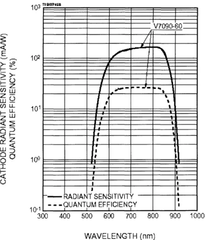
Intensifier gain and dynamic range can be improved by using a semiconductor material as the photocathode instead of a metal. Quantum efficiency improves by a factor of four over a broad range of wavelengths, resulting in higher gain. The sensitivity of a gallium-arsenide based photocathode is shown in Figure 2.15. This cathode has peak efficiency between 650nm and 850nm, and is well matched to the avalanche mode silicon light emitter with spectrum shown in Figure 2.9. Matching photocathode sensitivity to the light source
35
2.3. IMAGE INTENSIFICATION
Intensifier Gain vs # of MCPs 1 .UtI-+Ud 1.OE+07 = 1.OE+06 0 :1 1.OE+05 0 -r-1.OE+04 9 1.OE+03 1.OE+02 1.OE+01 0 1 2 3 MCPsFigure 2.13: Intensifier gain vs. number of MCPs
Resolution vs # of MCPs E 20 E E i 15 5 10 o 0 5 0 1 2 3 MCPs
103
H--z
--0UJ
Z
I U
On LLi--LL
Z LUz
0
T1 102 101 100 - RADIANT SENSITIVITY - - -' ANT IM FFFIINCY. I10-1f
F . " I..' .. 'I ----' -- ' I I
I
300 400 500 600 700 800 900 1000 WAVELENGTH (nm)Figure 2.15: GaAs Photocathode Sensitivity (Hamamatsu)
also improves rejection of spurious input signals and reduces background noise.
In the future, the image intensifier could be replaced by smaller or more efficient
struc-tures. MEMS micromachining might help to miniaturize the intensifier itself [48], and
aid in integrating the intensifier with a silicon integrated circuit. The large glass vacuum envelope could be replaced with a smaller vacuum package.
An up-converter might replace the intensifier if the efficiency of silicon light emitters were increased, or if efficient infrared emitters were integrated onto an IC. The up-converter converts photons at one wavelength to shorter wavelength, for example an infrared image can be converted to a visible one. A pixelless up-converter for mid-infrared imaging is described by Luo et al. [49]. It could eventually compete with image intensifiers, with the advantages of being smaller and requiring lower operating voltages.
2.4. CIRCUIT DESIGN FOR DISPLAYS
2.4 Circuit Design for Displays
The driver circuits for an electronic display are typically digital to analog converters which
convert stored digital data into into analog waveforms used to produce an image. Man-agement of leakage currents and device variation are key issues in data converter design.
Introductions to these topics are presented, followed by a survey of digital to analog
con-verter topologies and techniques, with emphasis on circuits for display applications. The
current copier is a circuit that uses a self-calibration technique to reduce sensitivity to
de-vice variation. Its basic concept is presented, along with potential advantages in the design
of display driver circuits.
2.4.1 MOS Transistors
Leakage Currents
Circuit techniques to reduce leakage currents have been proposed, for example a 12b
accu-rate analog storage cell [54]. Our design, as described in Chapter 4, uses circuit techniques
to minimize the effects of overlap capacitance and leakage currents on the current copier
circuit.
In the analog context, the main effect of leakage currents is to reduce circuit precision. An important property of CMOS circuits is their capability to store charge on floating nodes. The sample-and-hold circuit shown in Figure 2.17 is a widely used example of a charge-based circuit. An important figure of merit is how long it can retain a value within a specified level of precision. Non-ideal effects in the sample and hold circuit include
off-current through the switch, junction leakage through parasitic source/drain diffusions, and
charge injection due to overlap capacitance (CGD) of the switch device.
Gate and subthreshold leakage are serious problems for charge-based circuits such as the sample-and-hold. In charge-based circuits, the retention time is how long a circuit can
preserve a stored value within a specified level of precision. Long retention times allow the
circuits to function longer between calibration cycles, and reduce the amount of resources
spent on periodic calibration.
A transistor is often used as a MOS capacitor because gate oxide has the highest
ca-pacitance per area (fF/,um
2) of structures available in common CMOS processes. Charge
leakage through the gate limits the time period that a sampled value can be retained, and
changing device area does not remedy the problem because both capacitance and leakage
current are proportional to area. Poly-poly or metal-metal capacitors are available in some
processes, although their capacitance per unit area is much lower than the MOS capacitor.
Leakage test
NIIOS Vs--Vb=VdO -Die 0 8/02/0 achen
4 -n . . _ _ .... .... 1 ,UU-I Z 1.OOE-13
i 1.00E-14
1,00E-15 1 OOE-16 Efa1 0 0.5 1 1.5 2 Vg (volts)Figure 2.16: Gate current for an NMOS device
Gate leakage of a large 1.8 volt NMOS device was measured with a semiconductor
parameter analyzer at room temperature as shown in Figure 2.16. For this measurement the
source, drain, and bulk are at zero volts.
The resulting data are consistent with published results [50, 51], and the primary
mech-anism for gate leakage is direct tunnelling through the thin (32A) gate oxide. To assess the impact of gate leakage, consider a sample-and-hold implemented in this technology with a
voltage tolerance of lmV and a stored voltage around 1.OV.
I
C AV
(2.1)
area area
(2.1)
Current density at 1.OV is lOfA/,m
2and capacitance per unit area is 8fF/um
2. The
retention time is 800us. Display applications require retention times that are larger by
orders of magnitude. For example, a display operating at 100 frames per second with one
refresh cycle per frame requires a minimum retention time of 1/100 second, or 10ms. In a 0.18tim technology, one solution is to use thick-oxide transistors (70A vs. 32A) at circuit nodes where charge is stored. Thick-oxide transistors are available in most com-mercial CMOS processes. These devices have thicker gate dielectrics resulting in orders of magnitude less gate leakage. They also have larger minimum feature sizes and worse
high-frequency performance than thin oxide devices. Capacitance per unit area is lower
than for thin oxide devices, but still higher than other capacitor design options.
As CMOS processes scale to smaller dimensions and power supply voltages are re-duced, there is pressure to reduce the threshold voltage. Reducing the threshold voltage increases on-current due to a larger (VGS - VT) factor. However it also increases sub-threshold conduction by a factor of ten for every 90-100mv decrease in VT. This can be
I i i
Z011",
i i i 41 i i2.4. CIRCUIT DESIGN FOR DISPLAYS
39
I
Figure 2.17: Sample and Hold Circuit models. Left: ideal, Right: realistic
seen by setting VGS to zero in the equation for subthreshold conduction:
ID,OFF = Iseq(
- VT)/nkT(2.2)
In digital CMOS circuits, leakage currents cause static current to flow from from power
to ground. It increases power dissipation and causes reduced noise margins due to signal
degradation. In designs with millions of transistors per chip, leakage currents can exceed
the currents used in active operation. Negative gate drive (V < 0) and the "stacking effect" have been used to reduce subthreshold conduction currents [52, 53].
Device Variation
The design of high-performance data converters depends on an understanding of device
variation and how to manage it. Variation is caused by random fluctuations which
oc-cur during the manufacturing process, and affects both material properties (doping levels,
threshold voltage) and geometries (transistor width and length). The most commonly used
variation model for MOSFET threshold voltage and currents is of the form aID
- k[55]. Other models have also been proposed, i.e. [56].
Maintaining consistent image qualities across a display is a challenging problem, and
becomes even more difficult as integrated circuit feature sizes decrease. Traditional analog
designs use layout techniques such as symmetry and dummy devices to improve matching.
In a microdisplay, devices must be spread over a wide area and such techniques are not practical. To measure variation across large length scales, we designed an NMOS current mirror with 22 legs spanning 2.0 millimeters in the TSMC 0.18pm process. This struc-ture represents a realistic design for a microdisplay where drivers are spaced across a die. All devices were 2*2ipm in size. In a microdisplay, the currents through individual driver circuits are small because there are many operating in parallel. The input current was set
Die 0. ceumrrrt rlrrr VdmOi, M tLuA 1.2DE
1.10-
.
1~SH7 1 a 5 7 9 11 pIillenFigure 2.18: Current mirror measurements
at 1LA, and the drain voltage of mirror devices was 0.9V. Threshold voltage for NMOS devices is 380mV from simulation models, and the VGS corresponding to 1,uA is 495mV. The variation between output currents is aID = 2.5%. When there are 1,000 drivers on a chip, circuits should be designed at the 4a or 5a certainty level. This represents 3.5b pre-cision, far short of current application demands. Modem commercial display systems have 8b resolution, and 10-12b displays are being developed. To achieve reasonable resolution, circuit techniques to improve matching between display drivers will be necessary.
2.4.2 DAC Fundamentals
Digital to analog converters (DACs) are used in display systems to convert digital data into analog waveforms that control light emitters or light modulators. This section is survey of DAC circuit design techniques with emphasis on converters useful for displays.
An ideal unipolar voltage-mode DAC has an output range from zero volts to (2N - 1) *
VLSB volts. It accepts a digital data word d(N: 1) and performs the function:
N-1
VOUT = VLSB * i,
d(i)
* 2 (2.3)i=O
The output voltage is discrete, and quantization noise is: VQ,rms = VLSB/xV . Alter-natively, this can be expressed as the signal-to-noise ratio: SNR = 6.02N + 1.76 dB, where
N is the number of bits. Johns and Martin [57] provide a discussion of non-ideal behavior
in DACs.
DACs can be divided into two groups: Nyquist rate DACs that change their outputs once per cycle, and oversampling DACs that change their outputs multiple times per