Chopper Stabilization in Analog Multipliers
by
All
Hadiashar
Submitted to the Department of Electrical Engineering
and Computer Science
in partial fulfillment of the requirements for the degree of
Master of Science in Computer Science and Engineering
at the
MASSACHUSETTS INSTITUTE OF TECHNOLOGY
February 2006
@
Massachusetts Institute of Technology 2006. All rights reserved.
A uth or ...
...
,.
... ...
Department of Electrical Engineering
and Computer Science
January 31, 2006
Certified by...
...
...
Joel L. Dawson
Assistant Professor
Thesis Supervisor
Accepted by ..
. . . ... .. .. .. . . .. . .Arthur C. Smith
Chairman, Department Committee on Gradu
ents
MASSACHUSETS INSTITUTE
OFTECHNOLOGY
Chopper Stabilization in Analog Multipliers
by
Ali Hadiashar
Submitted to the Department of Electrical Engineering
and Computer Science
on January 31, 2006, in partial fulfillment of the
requirements for the degree of
Master of Science in Computer Science and Engineering
Abstract
The multiplier is a fundamental analog building block. Analog multipliers are used
in many systems such as filters, neural networks, automatic gain control circuits, and
phase alignment systems. As with any circuit, analog multipliers are plagued by DC
offsets. When considering techniques for removing this offset, the question of
con-tinuous regulation versus calibration arises. We can easily implement a calibration
method, however, how often one must calibrate becomes an issue. Additionally,
cali-bration typically forces the multiplier to suspend normal operation while the offsets
are being measured. In this thesis, a technique for continuously regulating offset in
multipliers is studied in isolation. Chopper stabilization, a technique long used in DC
amplifiers, is applied to analog multipliers to achieve the lowest offset reported.
Thesis Supervisor: Joel L. Dawson
Title: Assistant Professor
Acknowledgments
During my time at MIT, I have encountered many people that have helped and
supported me in the journey to completing this research and thesis and I am delighted
to be able to thank them here.
I would like to deeply thank my advisor, Professor Joel L. Dawson, for taking
a chance on taking me in as his first graduate student. It has been a tremendous
privilege and blessing to work with him. His technological knowledge and constant
encouragement has allowed me to complete my research successfully.
MIT is a great resource for experience and knowledge in any technical field. I
thank my fellow lab mates, as well as members of the Perrott, Sodini, Lee, and
Sarpeshkar group's for allowing me to use their knowledge and resources, time and
time again.
I would like to National Semiconductor Corporation for allowing me to use their
0.18pm process free of charge and for their design and fabrication support.
I have been lucky to have developed some close friendships that have the added
benefit of directly aiding me in my research here. I thank Ji-Jon Sit for his constant
advice and prayers from when I started at MIT, regarding course work and finding an
advisor. I also thank Colin Weltin-Wu, whose passion for analog circuits has allowed
me to have a deeper appreciation for circuit design.
Being in Boston and at MIT, I have made many friendships outside of my field
that have greatly enriched my time and experience. I thank the members of GCF
and Mosaic and my roommates for their help, advice, prayers, and impact that they
made in my life.
I would like to thank my parents for always loving and supporting me, even when
I decide to move 3000 miles away.
Lastly, I thank God for his constant faithfulness.
"Not to us, 0 LORD, not to us, but to your name be the glory, because of your
love and faithfulness." -Ps 115:1
Contents
1
Introduction
1.1
Motivation. . . . .
1.2
Organization
. . . .
2 Multiplier Core
2.1 Multiplication in Analog Circuits . . . .
2.2 Generalized Offset Model . . . .
2.3 Isolating Offset . . . .
3 Current Approaches
3.1
Overview of Current Techniques . . . .
3.1.1
Nonlinear Feedback . . . .
3.1.2
Floating-Gate Charge Injection . .
3.1.3
Digital Integrator in Feedback
.
. .
3.2
Calibration vs. Continuous Regulation
4 Theory of Chopper Stabilization
4.1
Application to DC Amplifiers . . . .
4.2
Application to Analog Multipliers . . . . .
4.2.1
Effects of Pseudorandom Chopping
4.2.2
Quadrature Chopping . . . .
5 Limits on performance
5.1 Residual Offset Model . . . .
13
13
13
15
15
18
19
21
. . . .
21
. . . .
21
. . . .
22
. . . .
22
. . . .
23
25
. . . .
25
. . . .
26
. . . .
28
. . . .
28
29
29
5.2
Nonidealities in Circuits . . . .
31
5.2.1
Clock Nonidealities . . . .
31
5.2.2
Chopper Nonidealities . . . .
32
5.2.3
Effects of DC content in Chopping Waveforms . . . .
32
5.2.4
Nonlinearities in Multipliers
. . . .
33
6 Prototype of Chopper Stabilization with
6.1
System Overview . . . .
6.2 Objectives . . . .
6.3 Circuit Details . . . .
6.3.1
Gilbert Cell . . . .
6.3.2
Choppers . . . .
6.3.3
Quadrature Clock Generators . .
6.3.4
Select Circuitry . . . .
6.4
Testing . . . .
Analog Multipliers
7 Conclusion
7.1
Future Work . . . .
A Experimental Setup
A.1 Input stage
. . . .
A.2 Output Stage . . . .
A.3 Chip Support Circuitry . . . .
A.4 Supplemental Information . . . .
35
35
. . . .
35
. . . .
36
. . . .
36
. . . .
40
. . . .
40
. . . .
41
. . . .
41
47
47
49
49
51
53
53
List of Figures
2-1 Two-Quadrant Multiplier . . . .
16
2-2 Four-Quadrant Multiplier
. . . .
17
2-3
Simple Multiplier ...
...
18
2-4 Three Offset Model . . . .
19
3-1
Block Diagram of Nonlinear Offset-Compensated Multiplier . . . .
22
3-2
Block Diagram of Cancelation Scheme
. . . .
23
4-1
Chopper Stabilization in Op-Amps . . . .
25
4-2 System Block Diagram . . . .
26
4-3 Chopping Waveforms . . . .
27
5-1 Six Offset Model . . . .
29
6-1 Block diagram of Chip . . . .
36
6-2
Gilbert Multiplier Cell . . . .
37
6-3
Gilbert Multiplier Cell with Biasing . . . .
39
6-4 Chopper Cell . . . .
40
6-5
Clock Generation Network . . . .
41
6-6
D ie Photo . . . .
42
6-7 D C Sw eep . . . .
43
6-8
Output Chopped Waveform . . . .
43
6-9
Output Spectrum . . . .
44
A-1 Test Board Layout . . . .
50
A-2 S/D Converter Schematic
. . . .
51
A-3 D/S Converter Schematic
. . . .
52
A-4 EagleCAD Layout . . . .
53
List of Tables
6.1
Multiplier Elements. . . . .
A.1 S/D Elements . . . .
A.2 Board Elements . . . .
40
51
Chapter 1
Introduction
1.1
Motivation
Analog multiplication is an important building block in many analog and mixed-signal
systems. In many applications, it is important to have one that can perform well as
to not limit performance of the entire system. For example, in a Cartesian feedback
power amplifier system, the sum of products IQ'
-
QI' is used in the control path
to compensate for phase misalignment. Any significant error in this calculation will
lead to instability in the linearization loop. The offset in the analog multipliers used
to calculate the IQ' and QI' products contributes greatly to this error [1].
Chopper stabilization applied to analog multipliers was first introduced in the
Cartesian feedback system of [1]. This investigation marks the first time that this
technique has been examined in isolation. Our purpose is to provide the first full
characterization of a chopper stabilized multiplier, and to establish a benchmark for
the multiplier offset performance.
1.2
Organization
This thesis begins with a clear explanation of the theory of the new multiplier
tech-nique, and culminates with measured results of a fabricated prototype. Chapter 2
introduces the multiplier and offset model that will be used throughout the thesis.
Multipliers are in general a nonlinear device with many nonidealities. It is therefore
important to have a linear model that is usable across an input range along with a
model to characterize the offset behavior of the multiplier.
A brief overview of current approaches are outlined in Chapter 3. Some thoughts
are also presented regarding the question of continuous regulation versus calibration.
The chopper stabilization technique is explained in Chapter 4. A review of the
technique applied to operational amplifiers is first explained followed by the
applica-tion to analog multipliers.
Chapter 5 provides a discussion of the limitations when applying the chopper
stabilization technique. As any technique is never perfect, nonidealities in the existing
and newly introduced blocks will cause undesired effects. These will be outlined so
as to provide guidance for a designer wishing to apply our technique.
An IC prototype of the chopper stabilization technique is described in Chapter 6,
along with results. We conclude with some closing words in Chapter 7.
Chapter 2
Multiplier Core
The multiplier cell, being a basic analog building block, has been subject to numerous
implementations and analyses in the literature. An excellent description of many
CMOS implementations is found in
[2].
For the purposes of our demonstration the
exact topology of the multiplier is not critical. Rather, the technique outlined in
Chapter 4 can be applied to any analog multiplier as long as it is a differential
implementation. In this chapter we will walk through an intuitive way to understand
the analog multiplier as well as a simple offset model.
2.1
Multiplication in Analog Circuits
Implementations of multipliers vary widely from single-ended to differential as well as
traversing the sub-threshold, linear, and saturation regions. To verify the
function-ality of the multiplier one must examine the drain equations of the MOS transistor.
This can often be very difficult, especially in the square-law regime of the saturation
mode. The exact analysis will be examined in section 6.3.1, but first this will be
approached in an intuitive manner.
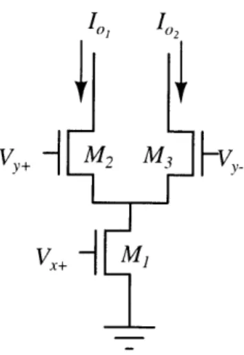
Starting with a basic differential pair as shown in figure 2-1, we can intuitively
get the functionality of an analog multiplier. Considering only small signals we can
designate V to be applied to M, as a single-ended signal and V. to be applied to
I
I
VA M2 M k V
V+ MI
Figure 2-1: Two-Quadrant Multiplier
a constant bias current is set by M
1which splits equally between the M
2and M
3branches. Now if we swing V strongly enough one way so that all of the bias current
flows only through one branch, we have in essence multiplied V by 1, which is Vy
in this case. When we swing V strongly enough the other way, we source all of the
bias current through the other branch and now multiplied V by -1,
inverting the
signal. We find that changing V linearly between these two values will also change
the output linearly as long as we do not violate the small signal approximations.
In the same way we can alter V, to change the bias current, which again linearly
changes the output as long as we are in the small signal mode. Vy can vary between
positive and negative values, while V is confined to positive values. Thus we have a
two-quadrant multiplier.
In order to get full four-quadrant multiplication, we must add a complimentary
circuit, as shown in figure 2-2, and apply V, differentially. We can see that when
we swing V strongly enough to draw all the current into one branch or the other,
this flips which top differential pair we choose and thus inverts our output giving
us four-quadrant multiplication. To first order this works, however, taking into full
account the square-law characteristics as well as any second-order effects, a good
amount of non-linearities are introduced into the system. If we are careful to stay
in the small signal regime of the transistors, we can minimize the non-linearities as
Vd M3 M4
h-
M5 M6 V,VY
V+ dMAl M2 kVX_
Figure 2-2: Four-Quadrant Multiplier
much as possible. While the analytical details can very widely, this type of reasoning
can be used to roughly understand a number of different topologies.
This structure in figure 2-2 is the Gilbert cell first developed as a bipolar circuit by
Barry Gilbert [3]. The analysis for this circuit works out very neatly, as it builds off
the exponential law of the bipolar transistor. A MOS implementation of this circuit
also works [4]. The Gilbert cell is the most widely used and analyzed multiplier cell
in analog circuits. Therefore we will use this in our demonstration for familiarity and
ease of understanding.
Figure 2-3 shows our basic multiplier core. It takes two inputs through an ideal
multiplier of gain k to one output. This is assuming we are operating in the linear
range of the multiplier. The equation for this setup is simply:
Vo = kV V
l
(2.1)
Mis-matches in resistor sizes, transistor W/'s and threshold voltages all contribute to the
LIoffset. If we look at the topology of the Gilbert cell, we see that it is comprised of
several differential-pair like structures. We can look at the input referred offset of the
differential-pair to get an idea of how the offset affects us [5].
1
FAR
A1
16|=|AVt|+
-(VGS
-Vt)+
(2.2)
2
[R
9
Looking at equation 2.2 we can see that the threshold voltage mismatch directly
affects the input referred offset, while the transistor
Wand resistor mismatches are
scaled by the over-drive voltage.
VX
VV
Figure 2-3: Simple Multiplier
2.2
Generalized Offset Model
In order to fully capture the offset behavior of the multiplier we need to define three
separate offsets, two for the inputs, 6, and Jy, and one for the output 6. Figure 2-4
shows this more complete model. We can now write out the equation for this new
model:
Vo = k (Vx + Jx )(Vy + Jy) + Jo
(2.3)
= kVVy + kV6 y + kVy6, + koxjy + J0
(2.4)
We still have our desired product VxVy, but now we have several artifact terms which
are the various products of the offset and input terms.
6X
V,
+
V,
+Figure 2-4: Three Offset Model
2.3
Isolating Offset
As is, it is difficult to measure the various offset 6's of the multiplier. To do so we
must be able to separate and isolate each component on its own. If we simply set
one input to zero and the other to a sinusoid of a known amplitude we can get the
following:
V, =0, Vj= Asinwt
(2.5)
Vo = (V + 6)(Vy+ 6)+6o
=
k(6x)(Asinwt
+ 6y)
+ 6o
=
(kA6xsinwt
+ k6x8y + 6
0)
(2.6)
At the output of the multiplier we now have the amplitude of the sinusoid carrying
the offset content of one input. We can perform the same test, switching the inputs.
At this step we will now have the offset information for both inputs. If we zero out
both inputs we will get the following output:
kor y + 60
(2.7)
Knowing 6, and 6y, we can subtract those out and get 60. We can make a much simpler
observation that 64, 6y, and 60 are all small and of the same order so equation 2.7 can
be approximated simply as 6o.
Chapter 3
Current Approaches
Mitigating offset has been a long-standing problem that many people have tried to at-tack. Common techniques include careful layout techniques such as common-centroid layout, inserting dummy devices, using devices with large gate areas, and reducing the over-drive voltage. It should be noted that employing these techniques can only re-duce the offset to some lower bound. In order to achieve lower offset some specialized circuit technique must be applied.
3.1
Overview of Current Techniques
Only a few papers have dealt with offset compensation techniques for multipliers. Their methods and applications vary greatly and we will briefly discuss them in this
section.
3.1.1
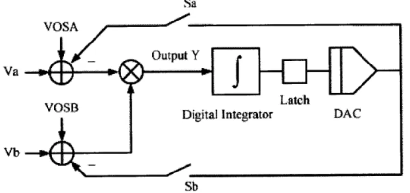
Nonlinear Feedback
One method uses two multipliers placed in feedback to extract and compensate for the offset [6]. To extract out the offset, it also extracts out any low-frequency content and thus removes any DC content from the signal. The block diagram for this method is shown in figure 3-1 [6]. The purpose of the second multiplier is to ensure that the feedback loop transmission remains negative. The goal of this method is to modulate
the offset content back to baseband with the second multiplier and to subtract it from the input. The low pass filter ensures that only the DC offset content is being subtracted. However, this only works if you have an AC signal. This is not a suitable method to be run continuously for DC multiplication.
Multiplier
Lowpass
Signal Input Out+ Offse Coeut-o -RefF
Lowpass -Ret FilterInu TOut+
RfIn+ Out-In.-Offset Compensator
Figure 3-1: Block Diagram of Nonlinear Offset-Compensated Multiplier
3.1.2
Floating-Gate Charge Injection
Another method utilizes the use of floating gate transistors at the input of the dif-ferential gate inputs [7]. Charge is injected onto the floating gate until the offset is canceled out. This technique requires a calibration step which will be further dis-cussed in section 3.2.
3.1.3
Digital Integrator in Feedback
To realize this method a digital integrator and a DAC are placed after the output and fed back to the inputs [8]. The block diagram for this system is shown in figure 3-2
[8]. The digital integrator block consists of a comparator and a counter. The digital
integrator collects the offset information and commands the DAC to supply an error compensating signal. This value is subtracted from the input until the feedback locks the offset to zero. This method can be run in two states: one is a calibration mode where the feedback is enabled for some time and the offset compensation value is stored on a coupling capacitor for use when the feedback is disabled. The other is run in the background continuously while the multiplier is in use. This, however, removes all DC content from the signal.
Sa
Va Output Y
Va
Latch
VOSB Digital Integrator DAC
Vb
Sb
Figure 3-2: Block Diagram of Cancelation Scheme
3.2
Calibration vs. Continuous Regulation
Considering the above techniques, as well as compensation techniques in general, the theme of calibration versus continuous regulation becomes an issue. It is not feasible to run the methods explained in this chapter continuously in the background if DC multiplication is the intended use of the multiplier. In order to use these methods for DC multiplication, both inputs must be grounded and the compensation technique enabled. The final offset compensation value to be injected at the inputs must then be stored on a capacitor for use during the computation cycle with the method disabled. As time elapses several factors will affect the offset. Some of these factors include temperature variations, load change, and leakage and/or voltage drift on the capacitor. The question now becomes how long can we wait before we must recalibrate again. In clocked applications it comes naturally to have a calibration
state, where one can have a sampling phase during one clock phase and a processing phase during the other. In applications where a clock is not easily integrated, a method to continually regulate the offset is necessary. In the following chapter we will outline a continuous method to compensate offset in analog multipliers.
Chapter 4
Theory of Chopper Stabilization
Chopper stabilization is a long-standing method of offset compensation used often for DC amplifiers [9]. Developed approximately 60 years ago, chopper stabilization was realized using vacuum tubes and mechanical relay choppers to achieve low-offset
DC amplifiers. In this chapter, we will review chopper stabilization applied to DC
amplifiers. We will then extend this method to analog multipliers.
4.1
Application to DC Amplifiers
The fundamental goal of chopper stabilization is to separate, in the frequency domain, the desired amplified signal from the artifacts of DC offset. To accomplish this, the input signal is first chopped or modulated to a higher frequency. The amplification operation is done free from error and the signal is chopped back down to baseband
C'C
CO. C.
AVC
Co
Figure 4-1: Chopper Stabilization in Op-Amps
25
k
V, 5
C
X
T
cx_
c,
Figure 4-2: System Block Diagram
by modulating with the same frequency. This is illustrated in figure 4-1. Here, c,
represents a square wave that alternates between -1 and + 1. The chopping operation is a simple one that can be realized easily with four MOS switches. The switches do
a simple commutation between -1 and
+1.
4.2
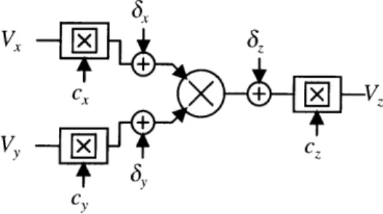
Application to Analog Multipliers
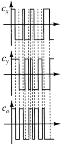
Chopper stabilization applied to analog multipliers was first introduced in a Cartesian feedback system integrated with a phase alignment system [1]. It may not be apparent how this method can be applied to analog multipliers but two modifications must be made. First, perform the up-chop operation with two orthogonal signals. Second, perform the down-chop operation with the product of the two up-chop signals. The system block diagram is shown in figure 4-2. We can understand this more clearly mathematically. Suppose we have two random square wave signals, c. and cy, as in figure 4-3, modulating between +1 and -1 that are orthogonal (i.e. uncorrelated), such that < c.cy >= 0. We set c, as the product of c., and cy. We can easily see by
graphical means that multiplying each chopping signal by itself will give unity. This leads to the following:
cxcO = cY (4.1)
cYcO = cx (4.2)
Cx
T
Figure 4-3: Chopping Waveforms
Now chopping the input signals with the appropriate waveforms and adding the input referred multiplier offset we find:
VcX + 6x (4.3)
VlcY + 6Y (4.4)
Applying these signals to the input of our idealized multiplier:
Vm = k(Vc, + 6,)(Vycy + 6y) (4.5)
= kVVycxcy + kV 3yc, + kV6xcy + k6e,
= kVVc, + kV65c, + kVyxcy + k 6 y (4.6)
We can now apply the output offset of the multiplier and perform the down-chop operation:
Vo = (VM+6O)co
= (kVVyco + kV6,ycx + kVy6xcy + k625y + 60)c, = kV Vycoco + kVx6ycc 0 + kV6,cyco + (k,6y + 6,)c,
= kV Vy + kVoycy + kV5xcx + (k6x3y + 6o )c, (4.7)
To the extent that we are able to perfectly implement chopper stabilization, we have
successfully separated the desired output, VXVy, from the offset artifacts. Taking a
closer look, we observe that there are three components to the output. Our desired output at baseband, combination terms consisting of the input and offset at each of the chopping frequencies, and offset terms at the down-chop frequency. We simply low pass filter the output to achieve the desired output.
4.2.1
Effects of Pseudorandom Chopping
If we have a perfectly random signal, its spectral content will be a flat white noise
distribution. The desired effect of the up-chop operation is to spread the input signals across all frequencies except DC, where the offset lies. At the output of the multiplier we have the product of the two inputs spread across the frequencies along with the combination offset and input terms carried at an uncorrelated white noise spectrum and the offset terms at DC. When we perform the down-chop operation, the desired product gets modulated back to DC and the offset artifacts are spread across the higher frequencies. Now this is true if we have perfectly random, uncorrelated signals. In practice it is very difficult to produce a purely random signal. Two signals that are random and uncorrelated is nearly impossible. This implies that the offset terms will not be perfectly separated from the output.
4.2.2
Quadrature Chopping
A specialized case of generalized pseudorandom chopping method is chopping the
inputs in quadrature. This gives us a down-chop frequency of ccy to be a signal at twice the input chopping frequency. At the output of the system we will have the de-sired output at DC, the combination input and offset terms at the chopping frequency in quadrature, and the pure offset terms at twice the chopping frequency. Generat-ing the quadrature clock is a straightforward procedure, which will be explained in section 6.3.3.
Chapter 5
Limits on performance
No technique is ever perfect and it is impossible to achieve zero offset. Imperfections in the chopping switches, chopping waveforms, and multipliers will all contribute to some residual offset. In this chapter we will define a new offset model that will take this residual offset into account as well as explore any nonidealities and other limits on performance.
5.1
Residual Offset Model
After chopper stabilization is applied there will be some residual offset. To take
account of this we can expand the model we defined in section 2.2. In this model we defined three offsets that will sit inside the choppers to take into account the offset
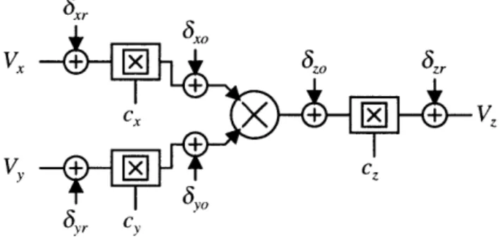
6xr xo V, + x 8o 8z,. CX
X
+
x
+
K,
V,
+
xCZ
Syr
C yFigure 5-1: Six Offset Model
due to the multiplier. In theory this offset should be modulated to a higher frequency due to the chopper stabilization. To account for the residual offset, we can define another offset term for each one we defined in section 2.2. To the previously defined offset terms we will add a subscript c for the offset that is chopped out. The new offset terms will have a subscript r for the residual offset left over after applying chopper stabilization. These residual offsets will be placed outside the choppers as in figure 5-1. Taking these newly defined offsets into account the signals applied to the inputs of the multiplier are now:
X = (Vx + 6xr)cx
+
6xc (5.1)Y = (Vy + 6yr)cy + yc (5.2)
The complete product is now:
Vm
= k
[(V
+
6xr)cx + 6xe ][(V + Syr)cy + 6yC] + 6oc = k(Vx + 6xr)(Vy + 6yr)Co+k(V + 6xr)6yccx + k(Vy + 6
yr)6xccy
+kxcjyc + 60C (5.3)
Vo = VmCo + 6or
= k(Vx + xr)(Vy + 6yr) + 6or
+k(V + 6xr)6yccy + k(V + 3
yr)SxcCx
+(k6xcyc + c0c)cO (5.4)
The underlined term is what we have left over at DC. Looking at that by itself:
VoDC =
k(Vx +
xr) (Vy+
8yr) + 6or(5.5)
We observe that this equation is of the same form as equation 2.3, so the same technique to isolate the offset outlined in section 2.3 still applies. These residual offsets are what we need to measure in order to characterize the performance of
chopper stabilization.
5.2
Nonidealities in Circuits
If we are able to perfectly implement chopper stabilization with a perfect clock and
a perfect switch we can achieve zero offset, or at least to the lower bound of the measurement equipment. As stated in the beginning of this chapter, this is impossible. In this section we will provide some discussion as to the nonidealities that may be the source of the residual offset.
5.2.1
Clock Nonidealities
Since the clock signals are the backbone to driving the chopper stabilization technique, it is crucial to ensure the clock signals are reliable. The first mode of concern is to ensure that the input chopping signals are truly orthogonal. With pseudorandom chopping, one way to get a pseudorandom signal is using a ROM so circuits are not an issue. Rather, the issue lies in the algorithm to produce the orthogonal random signals. If we use quadrature clocks, then this can be easily implemented with a few flip-flops. This will produce fairly accurate quadrature signals. However on the subject of offset, the inverters at the output of the flip-flops will have some input-referred offset. This will affect the switching transitions of the inverter. Let's suppose we have a 100mV input offset. This will shift the switching threshold lower for the input waveform and thus reduce the duty cycle. In turn a non-50% duty cycle will lead to some DC content at the output of the choppers.
Misalignment between the up-chop and down-chop wave forms may also lead to problems. This can be caused by phase shift in the multiplier or line delay between
the clock generation circuit and the choppers. However a phase misalignment of
#
will just lead to a cos# attenuation in the signal and not translate any offset back to baseband.
5.2.2
Chopper Nonidealities
The chopper cells are the additional circuitry that we are adding to our signal path, so any imperfections will directly affect our signal and offset. For our purposes we can model the chopper cell as being a perfect mixer that is mixing the input signal with
some non-ideal square wave that modulates between -1 and +1. Some of the effects
that we are concerned about are mismatched rise and fall times and mismatched switching peaks. Again these lead to a DC offset in the waveform. We will examine the effects of DC offset in the chopping waveforms in section 5.2.3.
5.2.3
Effects of DC content in Chopping Waveforms
From the previous sections we see that many of the nonidealities in our system will lead to a DC offset in the chopping waveforms. We will now see how these offsets ex-actly affect our performance. The offset in the chopping waveforms will be designated
by 6en and we will replace cn by (cn + 6c). We can now expand upon equation 4.5:
Vm k(V(cx +
6cx)
+6x)(V(cy + 6cy) + 6y)
k(Vcx + V 6, + 6x)(V cy + Vycy + 6Y)
k(Vcx + 6' )(Vy cy + Y' )
= kVxVyco + kV6 cx + kVy' cy + '' (5.6)
Where 6' is the lump of the offset terms. Now applying the down-chop operation:
Vo (VM+60)(co+6co)
- (kVVyco + kV'cx + kV6'cy + k'' + 6o)(co+6co)
= kVVy + (kV6' + kV3' co)cy + (kVy6' + kVx ' CO)CX
+(k6'6' + 6o + kVxV6eo)c0 +(k3'' +O>co (5.7)
The underlined term is the additional offset term left over at DC. The first observation that we can make is that this term will only be present if the down-chop waveform
has any DC content. If we expand all the offset terms out:
(k(V6jc + 6X)(VYc6Y + 6Y) + 60) co
(kVVyocx cy + kV6cx5y + kVy cy x + kox6y +
60)6co
(5.8)What we observe is that if we have any DC content in the chopping waveforms, the offset that we are trying to chop out goes straight through scaled by the value of this
DC content.
5.2.4
Nonlinearities in Multipliers
Considering the square-law characteristics as well as all of the second-order effects the
CMOS transistor is quite nonlinear. In order to realize multiplication we utilize the
square-law to give us the VV product in addition to higher-order terms. We then
employ a method to cancel out the higher-order nonlinear terms [2]. It is difficult
though to completely cancel all of the nonlinearities from the multiplier. Thus there will be a small amount of nonlinearity over the already small range of inputs to keep the multiplier in the linear region. Upon first consideration it may seem that when we implement chopper stabilization around the multiplier these nonlinearities will trans-late offset terms back down to baseband. We can take a look at this mathematically and see if this is the case.
Setting our multiplier as the three offset model defined in section 2.2 and our
chopping waveforms as ca, Cb, and co where co = cacb, we can designate our two
inputs as:
A = aca + 6a (5.9)
B = bcb+6b (5.10)
If we have a input nonlinearity of the form
f
(.) = x2 + x + c, we get:f(A) = a2
+
2ataca +62 + aca + 6a + c (5.11)f(A)
=
Aica+ Ao where A1 =a +
2aoa,
AO =a
2 + 62 + 6 + C f(B)=
b2+
2bsbcb +62+
bcb + 6b + c (5.13)f
(B)=
Blcb+ Bo (5.14) where B = b+
2b6b, Bo = b2 + 5 +6b + CPassing these inputs through the multiplier:
Vm
f (A)f (B)
= (AiCa + Ao) Bcb + Bo)
(AiBic, + AoBlcb + A1BoCa + AoBo (5.15)
Vo VC.o
=
A
1B
1 + AOBica + A1BoC + A0Boco (5.16)The value of interest is the value modulated to DC:
A1B1 = (a + 2aa)(b + 2bab) (5.17)
= ab + 2ab(Sa + 6b) + 4aboa6b (5.18)
In equation 5.18 we have our desired result of ab in addition to several other offset artifacts. If we did not introduce chopping, however, our final result will be A1B1 +
A0B1 + A1Bo + A0Bo with A1, A0, B1, B0 defined as above. By adding chopper
stabilization we actually improve the linearity of our multiplier!
34
Chapter 6
Prototype of Chopper Stabilization
with Analog Multipliers
We introduce the prototype chip for testing the chopper stabilization technique. The chip is developed and fabricated with the National 0.18pm CMOS process. This chapter outlines the objective in mind for the prototype as well as circuit details for each block in the system.
6.1
System Overview
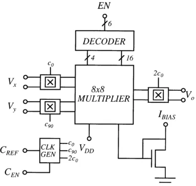
A block diagram of the prototype is shown in figure 6-1. The core of the system is an
8x8 array of multipliers. There is also a 6-to-64 bit decoder to select each multiplier individually in the array, a clock generation network to generate the quadrature clocks, and the input and output choppers.
6.2
Objectives
Our motivation in having an array of 64 multipliers is to extract a statistical sample of the offset performance across the chip. Offset will differ across the array due to variations across the die during fabrication. With this setup we will be able to get an average offset measurement across the span of the chip.
EN
6DECODER
CO 4 16 VX z 8x82coV,
MULTIPLIER
x
V
V,
C90'BIAS
CREF E o CENFigure 6-1: Block diagram of Chip
6.3
Circuit Details
6.3.1
Gilbert Cell
The multiplier core we chose is the Gilbert cell shown in figure 6-2. We already went through an intuitive analysis of this in section 2.1. Now we will go through an exact analysis of the multiplier. Starting with KVL between the two V, inputs:
Vx+ - VGS1 + VGS2 - Vx- = 0
V = VGS1 - VGS2 (6.1)
We can substitute in the drain equation:
ID k(VGs -VT) 2
VGS = + VT
k
(6.2)V
+0
A
4
14 V6VY+V M B 5T M y
Figure 6-2: Gilbert Multiplier Cell
Substituting into equation 6.1
'D1
(D2
+ VT- + VT)S
-k D1 - 'D2 (6.3) We know that: IB ID1 + ID2 ID2 B ~ ID1 (6.4) Continuing on:Vk1 ID1 2 ID1IB ID1+IB D1
2 D B -D1B'-- + I
I;3 - 2IB2 4
o
- I '-2+ I- 2IBVk1 +V
4k2
- D1 D4 'B ID12
I1,2 = '2VIB
B SIBV 1V~Vxki
BV 22
Lk
1 -V -_ 2(
k
1We can also write similar equations for drain currents 13, 14, 15, and 16:
13,4 1 1
2
k2(
5,6 12 '2
Now solving for the differential output current:
101 = I3 + 15 102 = 14 + 16 IOD = 101 - 102 = (13 + I5) - (14 + 16) = (13 - 14) + (15 - 16) (6.11) (6.12)
Finally, we can make the appropriate substitutions from equations 6.6, 6.8, and 6.10:
yk2 V -K k2 22 YV y~k 38 2 ID1-IB - I (6.5) (6.6) V k2
21,
V2 2 k V'12 2VV
k2 212 2 (6.7) (6.8) (6.9) (6.10) 2 '12v
2 22
K)
IOD 2 v'"2-VX )2 V \k1(
IB
I 2k 1 2
-VYk2
LV2
(6.13)
\k2
k
1V2&
Since V is small we can neglect V2.
Vo = IODR
2k
1k
2R Vx Vy (6.14)The full Gilbert cell with biasing appears in figure 6-3. In order to bias the multiplier
properly, we can design for a certain linear range while ensuring all devices are in
the saturation region. Based on equations 6.5, 6.7, and 6.9 we know that V < I
and V1 mtin(I1,12). A bias current of 200pA and a linear input range of about
300mV was chosen for the design. Vx and Vy were chosen to be .85V and 1.5 volts respectively. Table 6.1 shows the sizes of all the transistors.
R R IBIAS Vd M, M4 M, M, V, Vi V+d M, M2, V, ME MO
Figure 6-3: Gilbert Multiplier Cell with Biasing
Device Value MB 19.92/1.98
MO 40.08/1.98
M - M2 3.6/2.24
M3 - Al4 1.8/2.24
Table 6.1: Multiplier Elements
6.3.2
Choppers
The chopper cell is a fairly straightforward circuit. The purpose is to commutate the
input signal by +1 and -1 and thus to modulate the signal to a higher frequency.
This can be done very easily without introducing any additional offset into the system. The choppers are made up of four switches as shown in figure 6-4. They are minimum size as to introduce no additional capacitance.
VOW+
Vin+ Vin
VOW-Figure 6-4: Chopper Cell
6.3.3
Quadrature Clock Generators
To generate the quadrature clocks we need two flip-flops connected as shown in fig-ure 6-5. To achieve this we need a clock reference that is four times our desired chopping frequency. The flip-flops then divide down the reference clock on the rising edge of the clock to produce the quadrature clocks. Because the flip-flops transition
010 C90
-0 D
Q
DOPQo---
CO
Cref
-0" C90
Figure 6-5: Clock Generation Network
only on the rising edge of the clock, this ensures that the output will always be 50% duty cycle. To create the down-chop clock, a third flip flop was added in order to divide down the reference clock by two and thus at twice the chopping frequency. A more general way to do this is to XOR the two generated up-chop together which is the same as multiplying the two signals digitally. An enable signal is also used in order to disable the chopping to examine the DC behavior of the multiplier.
6.3.4
Select Circuitry
In order to get a statistical sample of the offset across the chip an array of 64 multi-pliers were put on the chip. However only one of these multimulti-pliers are connected to the inputs and outputs at a time by the means of switches. Thus a digital section of minimum sized gates is put in to select a single multiplier. There are six select signals, Eo - E5. Eo - E4 go into a 4-to-16 bit decoder and E - E6 go into a 2-to-4
bit decoder. E5 - E6 enables one of the four 4x4 quadrants of the multiplier core while EO - E4 enables one of the sixteen multipliers in each quadrant.
6.4
Testing
The die photo is shown in figure 6-6. First step is to verify functionality of the multiplier itself. In figure 6-7, we can see the DC sweep of the multiplier. We can get
Figure 6-6: Die Photo
the gain of the system from the slopes of these line or we can input a square wave
and measure the output amplitude of the square wave. From this we find k = -.
DC Sweep 200 0V = 150mV 150 - - V Y= 1 00mV V = 50mV 100- V = 0MV V = -50mV 50- V = -100mV -+--V = -150mV -50 ~ -100--150- --200i -150 -100 -50 0 50 100 150 V (mV) Figure 6-7: DC Sweep
Now with chopping enabled we should get complete separation of our desired product from the offset artifacts. Our chopping frequency is set to 10kHz. In figure
6-8 is the output of the chopper stabilized multiplier. Here we can see the various
modulated offset artifacts on top of our desired DC product. Figure 6-9 shows the spectrum of the output with chopper stabilization enabled. We can see the artifacts at odd harmonics of the chopping frequency at 10kHz, 30kHz, 50kHz, and 70kHz. We can also see the artifacts of the even harmonics of twice the chopping frequency at 20kHz and 60kHz. There is some clock feed-through at 40kHz and 80kHz and an artifact at 57kHz due to connecting the signal generator to the clock reference input.
F:Output Chopped Waveform
oo--4
Figure 6-8: Output Chopped Waveform
Output Chopping Spectrum -30 -- -40- -50- -60-E I -70. I -801 90 -0 0 20 30 40 50 60 70 80 90 100 kHz
Figure 6-9: Output Spectrum
To characterize our performance we measure the offset values discussed in sec-tion 5.1. In order to measure J, we use the method outlined in secsec-tion 2.3, where we zero out the outputs and measure the output offset directly. We pass the output of the multiplier through a LPF in order to filter out the chopping artifacts. We hook up the output of the LPF to a Keithley 2001 DMM, which can measure 71 digits from 200mV. The DMM also has some averaging in order to get rid of any noise. We take two measurements, one for each polarity of the DPDT switch at the output of the chip (see appendix). Taking the sample across the 64 multipliers, we found the output offset to be a mean of 204pV, with a standard deviation of 23pIV, and a low of 159pV. The distribution of this data is shown in figure 6-10. This is a 1-2 order of magnitude reduction from the original output offset measured.
We can also measure the input offsets, 6, and 6J, by setting one input to a 1kHz sinusoid with an amplitude of 100mV and the other to zero. We look at the output of the multiplier through a signal analyzer and examine the artifact at 1kHz. This corresponds to the amplitude content specified in section 2.3. From this we measure a J. of 850nV and a 6y of 150nV. This is about an order of magnitude reduction from the original offsets measured.
1 b.14 0.16 0.18 0.2 0.22 8 (mV) 0.24 0.26 0.28 Figure 6-10: 3, distribution 45 Fkdata] 5-0 5 2 1
Chapter 7
Conclusion
Analog multiplication will continue to be an integral part of analog circuits. It is therefore important to have a collection of tricks that one can pull from to improve performance. In this thesis the performance of a technique for compensating offset in analog multipliers is verified and examined. At least one order of magnitude of reduction is achieved. Many limitations of the multiplier are also discussed. This is important for analog designers to keep in mind when considering this technique.
7.1
Future Work
Despite the simplicity of this technique there is still a lot of interesting work to be done. Although the pseudorandom chopping technique was introduced in Chapter 4, this was not examined experimentally. It would be very interesting to see how pseudorandom chopping compares in performance to quadrature chopping. The im-portance of having a purely orthogonal signal and how this affects performance needs to be examined.
Although the nonlinear feedback technique described in section 3.1.1 is not appli-cable to DC multiplication, it can be integrated with chopper stabilization to form
an interesting system1. This method would involve down-chopping with each of the
up-chopping waveforms in parallel with the original one and feeding each one back to 1
Idea suggested by Prof. Rahul Sarpeshkar
the respective inputs. Since the input is now modulated to the chopping frequency, the feedback will null out only the offset content. This method combines the ben-efit of separating the offset terms from the desired output, as well as providing the attenuating loop gain factor of feedback.
Appendix A
Experimental Setup
This appendix describes the experimental board setup. The board is 4 by 6 inches and consists of 4 layers. The top and bottom layers are signal layers and the second and third layers are a ground plane and a power plane. A block diagram of the board is shown in figure A-1. The blocks of interest are the input stage, output stage, and the chip support circuitry. Each block along with appropriate circuit diagrams will be described in this section.
A.1
Input
stage
The input stage consists of a BNC input jack and a DC voltage divided from the supply voltage that is multiplexed by a SPDT switch. This way we can easily switch between inputting an AC signal and a DC voltage. The DC voltage is pulled of a three resistor divider of the ±2.7 supply. The middle resistor is a potentiometer with the middle lead being the output.
Since external sources typically supply single-ended outputs and all of the input signals on the chip are differential we also have a single-ended-to-differential converter. The need for DC and low-frequency makes a transformer implementation not practical due to core saturation. The S/D converter is shown in figure A-2. The amplifiers cause the input voltage to be dropped across the resistor R. This causes a current to flow through the load resistors and provides a differential output at the load resistors. The
+1.8V +1.8V +1.8V +2.7V -2.7V +2.7V -27SID
-2.7V
1
Crystal Oscllto +1.8V RB D/S -0 +1.8V +1.8V +1.8VFigure A-1: Test Board Layout
resistor Rs can be trimmed for the appropriate common mode voltage at the output. For the V input this needs to be trimmed for a common mode voltage of 850mV and for the V, input a common mode voltage of 1.5V. For testing it is necessary to be able to provide zero differential voltage. This is done by simply shorting the output nodes together. The resistor values for each element are shown in table A.1.
50
Vx 'BIAS
MITCHOP V,
+2.7V +2.7V RL RL +0 + + _L + VIN R +2.7V R Re RS Ri ~~ -2.7V fRs -2.7V
Figure A-2: S/D Converter Schematic
Device Value Kx V R 68K 48K RL 36K 24K RE 30K 30K Rs 6K 6K RA 110K 110K Table A.1: S/D Elements
A.2
Output Stage
The output stage consists of a DPDT switch and an differential-to-single-ended con-verter block. Again for the same reason as the input stage, the chip provides a differential signal which must interface with the single-ended inputs of the lab equip-ment. This D/S conversion can be achieved with an instrumentation amplifier. The instrumentation amplifier, shown in figure A-3, consists of two buffer op-amps and a third op-amp connected in a subtracter configuration. We can then connect an
V1 +--R3, R +
o
LR2 R LR4Figure A-3: D/S Converter Schematic
cilloscope directly to the output of the D/S converter. To interface with a spectrum analyzer we also have a buffer to provide a low impedance output. The D/S block also feeds into a low pass filter to filter out the high frequency artifacts to then be measured with a pV DMM.
Many of these circuits have offsets of their own. Offset is what we are trying to minimize, however, and thus introducing any additional offset is unacceptable. To account for this we have a DPDT connected so that it inverts the signal applied to the D/S converter. If the output stage has an input referred offset of V8 we can then make the following two measurements:
Vmeasi = Vsig + Vos (A.1)
Vmeas2 -Vsi 9 + Vos (A.2)
We then take the two measurements and extract the signal as follows:
Vmeasi - Vmeas2 -
v(
2 = sig (A -3)
A.3
Chip Support Circuitry
There are some minor circuits also needed on the board for the chip to function properly. There are some simple pull-down switches for the multiplier select circuitry as well as an enable switch for the chopping clock. The reference clock can be attained from either a crystal oscillator on board or by an external source through a BNC cable. There is also a 27.5kQ resistor for the multiplier bias current.
A.4
Supplemental Information
Figure A-4 is a layout from EagleCAD of the board. In table A.2 are all the component values used on the board.
Figure A-4: EagleCAD Layout
R1 68K Ri 24K R21 27K R31 1K R2 36K(pot) R1 2 110K R22 470 R32 1K R3 36K R13 110K R23 30 R33 1K R4 110K R14 30K R24 220K R34 2K(pot) R5 110K R15 30K R25 22K R35 2K(pot) R6 30K R16 6K(pot) R26 22K R36 8.2K R7 30K R17 1K R27 22K R3 7 8.2K R8 6K(pot) R18 1K R2 8 22K R3 8 8.2K
Rg
48KRig
1K R29 22K R39 8.2KRio
24K(pot) R20 1K R30 22KTable A.2: Board Elements
54
9 GND VYN VYP VXN XP AVDD 4
/
16 GND NC VON VOP IBIAS GND E0 El 24 E2 E3 GND GND 2 1Figure A-5: Bonding Diagram
Also in figure A-5, is the bonding diagram for the fabricated IC.
55 GNDU DVDDa CLKREF 12 1 CLKEN E4 E,
Bibliography
[1] J.L. Dawson and T.H. Lee. Automatic Phase Alignment for a Fully Integrated
Cartesian Feedback Power Amplifier System. IEEE Journal of Solid-State Cir-cuits, 38(12), December 2003.
[2] G. Han and E. Sainchez-Sinencio. CMOS Transconductance Multipliers: A Tuto-rial. IEEE Transactions on Circuits and Systems II, 45(12), December 1998.
[3] B. Gilbert. A Precise Four-Quadrant Multiplier With Subnanosecond Response.
IEEE Journal of Solid-State Circuits, 3(4), December 1968.
[4] J.N. Babanezhad and G.C. Temes. A 20-V four-quadrant CMOS analog multiplier. IEEE Transactions on Circuits and Systems, 20(6), December 1985.
[5] Paul R. Gray, P.J. Hurst, S. H. Lewis, and R. G. Meyer. Analysis of Analog
Integrated Circuits. John Wiley & Sons, INC., New York, NY, fourth edition,
2001.
[6] M.T. Dastjerdi and R. Sarpeshkar. A Low-Noise Nonlinear Feedback Technique
for Compensating Offset in Analog Multipliers. IEEE International Symposium on Circuits and Systems, 1, May 2002.
[7] F. Adil and P. Hasler. Offset Removal From Floating Gate Differential Amplifiers
and Mixers. The 2002 45th Midwest Syposium on Circuits and Systems, 1, August
2002.
[8] X. Wang, Z. Shi, and S. Sonkusale. A Robust Offset Cancellation Scheme For
Analog Multipliers. Proceedings of the 2004 11th IEEE International Conference on Electronics, Circuits and Systems, December 2004.
[9] C.C. Enz and G.C. Temes. Circuit Techniques For Reducing The Effects Of Op-Amp Imperfections: Autozeroing, Correlated Double Sampling, And Chopper
Stabilization. Proceedings of the IEEE, 84, 1996.