HAL Id: hal-01078069
https://hal.archives-ouvertes.fr/hal-01078069
Submitted on 26 Jun 2018
HAL is a multi-disciplinary open access
archive for the deposit and dissemination of
sci-entific research documents, whether they are
pub-lished or not. The documents may come from
teaching and research institutions in France or
abroad, or from public or private research centers.
L’archive ouverte pluridisciplinaire HAL, est
destinée au dépôt et à la diffusion de documents
scientifiques de niveau recherche, publiés ou non,
émanant des établissements d’enseignement et de
recherche français ou étrangers, des laboratoires
publics ou privés.
Spectroscopic and structural investigation of undoped
and Er3+ doped hafnium silicate layers.
Larysa Khomenkova, Yong Tao An, Dimitri Khomenkov, Xavier Portier,
Christophe Labbé, Fabrice Gourbilleau
To cite this version:
Larysa Khomenkova, Yong Tao An, Dimitri Khomenkov, Xavier Portier, Christophe Labbé, et al..
Spectroscopic and structural investigation of undoped and Er3+ doped hafnium silicate layers..
Physica B: Condensed Matter, Elsevier, 2014, 453, pp.100-106. �10.1016/j.physb.2014.03.087�.
�hal-01078069�
Spectroscopic and structural investigation of undoped and Er
3 þ
doped
hafnium silicate layers
L. Khomenkova
a,b,n, Y.-T. An
a, D. Khomenkov
c, X. Portier
a, C. Labbé
a, F. Gourbilleau
aaCIMAP CEA/CNRS/ENSICAEN/UCBN, 6 Blvd. Maréchal Juin, 14050 Caen Cedex 4, France bV. Lashkaryov Institute of Semiconductor Physics at NASU, 41 Pr. Nauky, Kyiv 03028, Ukraine cTaras Shevchenko National University of Kyiv, Faculty of Physics, 4 Pr. Hlushkov, Kyiv 03022, Ukraine
Keywords:
Hafnium silicate films, Erbium,
Photoluminescence, TEM, Raman scattering, FTIR.
a b s t r a c t
This paper demonstrates the functionality of radio-frequency magnetron sputtering for the fabrication of undoped and Er-doped Si-rich-HfO2films with specific structural and spectroscopic properties. The
effect of post-deposition treatment on film properties was investigated by means of Fourier-transform infrared spectroscopy, Raman scattering and photoluminescence methods, as well as Transmission Electron microscopy. It was observed that annealing treatment at 850–1000 1C causes phase separation process and the formation of HfO2, SiO2and pure Si phases. This process stimulates also an intense light
emission in the 700–950-nm spectral range under broad band excitation. The phase separation mechanism as well as the nature of radiative transitions were discussed. Photoluminescence was ascribed to carrier recombination in silicon clusters and host defects. The appearance of silicon clusters was also confirmed by the comparison of luminescent properties of pure HfO2, SiO2, Si-rich-HfO2and
Si-rich-SiO2films. Additional argument for Si clusters’ formation was obtained under investigation of
Er-doped Si-rich HfO2films. These latter demonstrated 1.54-mm Er3 þ luminescence under non-resonant
excitation originating from an energy transfer from Si clusters towards Er3 þions.
1. Introduction
Hafnia-based materials are mainly considered as alternative dielectrics to SiO2in Si-based CMOS technology[1–3]. Along with
promising electrical properties, HfO2has a high optical
transpar-ency in the ultraviolet-infrared spectral range, high refractive index (2.0–2.1 at 1.95 eV), wide optical bandgap ("5.8 eV) and low phonon cut-off energy ("780 cm# 1) offering a low
probabil-ity of phonon assisted relaxation. Despite these advantages, spectroscopic investigation and optical applications of HfO2-based
materials are not numerous[4,5].
Intrinsic luminescence of pure HfO2is usually observed at 4.2–
4.4 eV and ascribed to self-trapped exciton[6,7], whereas visible emission (2.5–3.5 eV) is attributed to different oxygen vacancies with trapped electrons[6]. An emission of HfO2materials doped
with rare-earth elements was also demonstrated [8,9], but the mechanism of the excitation of rare-earth ions and their interac-tion with the host defects were not clarified.
The development of rare-earth doped materials suffers from their lower absorption cross-sections for 4f–4f transitions (10# 18–
10# 20cm# 2) and requires high-power excitation sources.
Mean-while, 4f–5d transitions have higher cross-section ("10# 12cm# 2),
but corresponding excitation levels belong to UV and vacuum UV spectral range, restricting many applications of these materials. Thus, to enhance an excitation of 4f–4f transitions, a host mediated excitation via energy transfer is needed.
Trivalent erbium ion (Er3 þ) is one of the most popular
lanthanides due to its radiative transitions in the green (4S 3/2 -4I
15/2, 558 nm) and in the infrared (4I13/2-4I15/2, 1.54 μm) being
extensively used as an eye-safe source in atmosphere, laser radar, medicine and surgery (4I
11/2-4I13/2)[10,11]. Earlier, a lot of efforts
have been concentrated on Er3 þ-doped Si-rich-SiO
2materials[12– 14]. An enhancement of Er3 þabsorption cross-section from
10# 21cm# 2[15] up to 10# 16cm# 2[13,14]was achieved due to
an effective energy transfer from Si-nanoclusters (Si-ncs) towards Er3 þions under visible broad-band excitation. Only a few studies
of Er-doped SiO2–HfO2materials were reported[8,16,17], whereas
Er3 þion excitation mechanism was not considered well.
In this work we present the results of a spectroscopic investi-gation of different HfO2-based materials, i.e. pure and Si-rich HfO2
materials (either undoped or doped with Er3 þions). The effect of
annealing treatment on the formation of Si-ncs in Si-rich HfO2
nCorresponding author at: V. Lashkaryov Institute of Semiconductor Physics at
NASU, 41 Pr. Nauky, Kyiv 03028, Ukraine.
host as well as the interaction mechanism of Si-ncs, Er3 þions and
host defects are investigated to achieve and to control light emitting properties of these materials.
2. Experimental details
The layers investigated were grown RF magnetron sputtering of pure HfO2target (99.9%) topped by calibrated Si and/or Er2O3chips
on pure Si and fused quarts substrates. Both types of substrates were placed on the same sample holder to obtain the layers grown at the same conditions. Before deposition, all Si wafers were etched in 10%-water HF solution to remove thermal SiO2 layer
from their surface. Substrate temperature was kept at 100 1C. The films were deposited in pure argon plasma with RF power density of 0.74 W/cm2during 200 min. The thickness of all films
investi-gated was about 850 nm. After deposition, the wafers were cut on 1 $ 1 cm2 pieces. Thermal treatments of the samples were
per-formed in a conventional furnace in nitrogen flow at TA¼800–
1100 1C and tA¼10–60 min. Besides, pure and Si-rich SiO2 films
were grown by similar approach from a pure SiO2target (99.99%)
and processed with the same conditions. More experimental details can be found in Ref. [3]. This allowed a comparative investigation of Si-ncs formation in Si-rich HfO2 films and
Si-rich-SiO2films to be performed.
The microstructure of the layers was analyzed by means of Fourier-transform infrared (FTIR) spectroscopy. The spectra were recorded in the range of 600–4000 cm# 1using a Nicolet Nexus
spectrometer under normal and Brewster angle (651) configura-tion. Raman scattering spectra were investigated with back-scattered geometry using a dispersive Raman spectrometer equipped with a CCD camera and a laser source at 532 nm. Transmission electron microscopy (TEM) was used to observe the evolution of the film structure with annealing. Photolumines-cence (PL) and PL excitation (PLE) spectra in the 200–800 nm
spectral range were studied with a Jobin–Yvon Fluorolog3-22 setup equipped with a Xe lamp as excitation source and a R928 photomultiplayer tube. All measurements were performed at room temperature.
3. Results and discussion
3.1. Microstructure of the samples versus annealing treatment FTIR and Raman scattering spectra we measured to study the microstructure evolution of the films with thermal treatment. Both methods allowed following the phase separation process upon annealing.
Fig. 1 represents the FTIR spectra obtained for as-deposited (AD) and annealed samples. AD samples show two broad bands (Fig. 1a and b). One of them, detected in the range of the 500– 700 cm# 1, is caused by Hf–O vibrations [18–25]. Usually,
amor-phous films show a broad Hf–O vibration band [18–20,25], whereas their crystalline counterparts demonstrate the peaks at 760–780 cm# 1, 640–670 cm# 1 and 500–560 cm# 1 [20,23–25].
Precise spectral positions and corresponding intensities of these bands depend on the HfO2crystalline nature (monoclinic,
tetra-gonal, orthorhombic or cubic)[24,25].
Another vibration band, observed for AD films, locates at "1010–1030 cm# 1 (Fig. 1a) and 940–960 cm# 1 (Fig. 1b). It can be ascribed to Hf–Si–O stretching vibration mode taking into account the transformation of FTIR spectra of pure HfO2 films
with Si incorporation towards HfSiOxhost formation[2,20,27].
Thermal treatment at TA¼800–950 1C and tA¼60 min causes
an increase of the intensity of O–Si–Hf band and its spectral shift up to 1070–1080 cm# 1, while Hf-O vibration band remains
unchanged (Fig. 1a and b). FTIR spectra of the films annealed at TA¼1000 1C and tA¼60 min show several peaks at about
670 cm# 1and 760 cm# 1(Fig. 1a) and 560 cm# 1, 650 cm# 1 and
760 cm# 1 (Fig. 1b) that are due to Hf–O vibrations [20,24–27].
Besides, the bands centered at 820 cm# 1, 1090 cm# 1 and
1250 cm# 1(Fig. 1a) and at 820 cm# 1, 1085 cm# 1and 1210 cm# 1
(Fig. 1b) are also observed. They can be explained by the different optical SiO2phonons[2,28,29]. This evolution of FTIR spectra can
be caused by a phase separation process leading to the formation of SiOxand HfOxphases. However, the shoulder at about 950 cm# 1
could be an evidence of the presence of HfSiOxphase in the films
annealed at TAo1000 1C, meaning that the phase separation is not
complete. An annealing at TA¼1100 1C and tA¼60 min results in
the narrowing of all vibration bands as well as in the disappear-ance of the shoulder at 950 cm# 1that reflects a complete phase
separation process (Fig. 1).
The effect of the duration of annealing treatment on FTIR spectra was also studied. The analysis of the spectra measured at Brewster incidence was performed because it gives more details on the evolution of FTIR spectra with annealing. As one can see fromFig. 2a, the shift of Hf–Si–O peak position (observed at about 1030 cm# 1 for AD film) is more pronounced for the samples
annealed at TAZ950 1C, whereas lower annealing temperature
does not affect this peak position. The increase of tAup to 15 min
results in a pronounced shift of Hf–Si–O peak position to higher wavenumbers (Fig. 2a) as well as a significant increase of its intensity (Fig. 2b). This demonstrates that the main variation of FTIR spectra occurs at short-time treatment (r15 min) that is in agreement with the results of our earlier work[20]. At the same time, longer annealing time results in a slight shift of this peak (less than 2 cm#1) (Fig. 2a). The analysis of FTIR spectra shows also the
decrease of intensity of 950-cm# 1 shoulder (considered as a
contribution of the HfSiOxphase) and its vanishing for TAZ1000 1C.
Along with this, the magnitude of 530 cm# 1 band decreases,
whereas the bands at 665 cm# 1and 770 cm# 1appear and increase
in intensity (Fig. 2b). However, no significant variation of these peaks’ positions was observed. This behavior of FTIR spectra means that there are two steps of the evolution of samples’ microstructure. Short-time treatment results in the formation of SiOx and HfOx
phases, whereas longer annealing causes the crystallization of HfO2
phase and further SiOxdecomposition. However, it is worth to note
that the films annealed at TA¼800–950 1C, whatever tA,
demon-strate the HfSiOxphase stability (Fig. 2a).
Raman scattering experiments of AD and annealed films were carried out to obtain additional information about microstructure evolution. For this purpose, the films deposited on Si and quarts substrates were investigated. Since corresponding Raman scatter-ing spectra were found to be similar, hereafter we will discuss the spectra of the films grown on quarts wafers to eliminate the contribution of Si TO-phonon mode observed usually at 521 cm# 1. Fig. 3shows only a broad band with a maximum at "499 cm# 1
for AD samples. Upon annealing at TA¼800 1C, this peak position
shifted up to "502 cm# 1(Fig. 3) that can be due to the formation
of rather pure silicon phase than HfO2phase. In fact, HfO2related
phonons are usually observed at 115 cm# 1, 295 cm# 1, 470 cm# 1,
595 cm# 1and 665 cm# 1(for tetragonal phase) and at 123 cm# 1,
146 cm# 1, 257 cm# 1, 316 cm# 1, 390 cm# 1, 496 cm# 1, 570 cm# 1,
623 cm# 1 and 660 cm# 1 (for monoclinic phase) [22–26]. It is
worth to note that the band peaked either at 470 cm# 1(tetragonal
phase) or 498 cm# 1(monoclinic one) are the most intense phonon
responses (Fig. 3). Since any formation of nanocrystalline or amorphous phase results in the broadening and low-energy shift of the phonons of bulk material, one can expect that nanocrystal-line HfO2phase have to follow this prediction [26,27]. Since the
contribution of bulk Si TO phonon is eliminated, and SiO2phonon
is peaked at "495 cm# 1(Fig. 3) and the HfO
2related phonons are
not observed at 500–525 cm# 1, one can conclude that the peak
observed at 502 cm# 1for the film annealed at T
A¼800 1C is due to
Si TO phonon and attests for the formation of pure Si phase. Higher annealing temperatures result in a continuous shift of the Raman peak position up to 516 cm# 1(T
A¼900 1C) as well as an increase of its intensity. This behavior can be ascribed to the formation of Si clusters as well as to the increase of their sizes and density. Their mean size was estimated to be 3.7–4.0 nm using the model described in Ref.[30].
Further TAincrease up to 950–1100 1C results in the enhancement
of Raman signal intensity as well as in the appearance of well-defined peaks at 455 cm# 1, 506 cm# 1, 523 cm# 1, 560 cm# 1,
575 cm# 1and 625 cm# 1. Higher T
Avalues result in the enhancement
Fig. 2. (a) Effect of annealing conditions on the peak position of Hf–Si–O vibration band. The values of TAare given in figure. The points at tA¼0 min correspond to AD films. (b) Variation of the intensities of different vibration bands corresponding to Hf–Si–O (1030 cm# 1and 950 cm# 1) and Hf–O (530 cm# 1, 665 cm# 1and 770 cm# 1) vibration
of all phonon modes as well as in the variation of their relative contribution to the spectrum (Fig. 3). All these bands correspond to the crystallized HfO2phase, but some of them are overlapping with
the Si TO phonon mode, hampering to conclude about the evolution of Si clusters’ distribution (Fig. 3). To reveal the presence of Si clusters, cross-sections of annealed samples were observed by TEM.
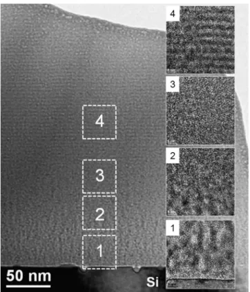
Fig. 4 presents a high-resolution TEM image of the sample annealed at TA¼950 1C and tA¼60 min and showing the brightest
PL emission. It is clearly seen some peculiarities of phase separa-tion in the film volume. An irregular structure is observed in the film depth close to the film/substrate interface (Fig. 4, image 1). Dark grey regions are due to HfO2phase, whereas white regions
are due to SiO2, respectively. Light grey regions, separating both
phases, can be due to either pure Si phase (or SiOxphase with high
Si content), or HfSiOx phase, considering the relatively large
volume of this phase. The structure in the middle part of the film (image 3) appears to be unaffected by the thermal treatment. This can explain the significant contribution of Hf–Si–O vibration bands in FTIR spectra of samples annealed at TA¼950 1C (Figs. 1 and 2). The cross-section of upper regions showed the formation of alternated layers with different contrasts that can be related to the formation of Hf-rich and Si-rich layers (Fig. 4, image 4). Observed features of the structure can be explained taking into account the possible mechanism of HfSiOxdecomposition.
Several mechanisms are known to explain the processes of material decomposition. One of them is Ostwald ripening that described the change of an inhomogeneous structure over time, when some clusters (grains) grow, only to be later dissolved, and other clusters are increasing in size due to the diffusion of corre-sponding species[31]. However, the initial formation of the micro-scopic clusters involves a large free energy barrier, and so can be very slow. Contrary to Ostwald ripening, spinodal decomposition is the mechanism for the rapid unmixing of a mixture of liquids or solids from one thermodynamic phase[32,33]. A clustering reaction occurs in a homogeneous, supersaturated solid solution, which is unstable against infinitesimal fluctuations in density or composition. This solution therefore separates spontaneously into two phases, starting with small fluctuations and proceeding with a decrease in the Gibbs energy without a nucleation barrier[32,33]. It is known that HfSiOx
materials have a metastable miscibility gap due to the covalent nature of Si–O bonds on one hand and ionic nature of Hf–O ones, on the other hand. The decrease of film free energy occurs usually through a phase separation process between HfO2-rich and SiO2-rich
phases [34] when the HfO2 phase forms at first. Thus, Ostwald
ripening could not explain the formation of alternated multilayer structure in our films. At the same time, spinodal decomposition supposes the existence of compositional wavelength, λC, in the
mixture, causes multilayer formation. This λCvalue, can be defined
as an average distance between the centres of two successive HfO2
-rich layers[34]and for our films λCwas found to be about 4–5 nm.
For very thick films (compared to bulk materials), this compo-sition wave starts to form at their surface and decays towards the volume. However, the substrate/film interface stimulates also formation of composition wave. Thus, the interaction of the waves penetrating in opposite directions, i.e. from film/substrate inter-face towards film surinter-face and vice versa[34], will determine the result of the phase separation. The formation of alternated layer structure close to the film surface is an evidence of significant role of the surface in the phase separation process.
Fig. 3. Evolution of Raman scattering spectra of Si-rich HfO2films with annealing
temperature measured for the samples grown on quarts substrate. Corresponding spectrum for quartz substrate is presented for the comparison. The TAvalues are
presented on the figure; tA¼60 min.
Fig. 4. Cross-sectional bright-field TEM images of the sample annealed at 900 1C. The images 1–4 represent magnified sections of different regions of the film depth.
Besides HfO2and SiO2phases, light grey regions separating the
two phases were also observed (Fig. 4, images 1,2). They can correspond to either pure Si phase (or SiOxphase with low amount
of oxygen), or HfSiOx phase, considering the relatively large
volume of this phase. From the comparison of FTIR (Figs. 1 and 2) and Raman scattering data (Fig. 3), one can suppose that the contribution of silicon-rich phase exceeds that of HfSiOx. It is
interesting to notice that the diameters of light-grey regions do not exceed 5 nm (Fig. 4). This is in agreement with Si-ncs mean size estimated from Raman scattering spectra (Fig. 3). However, any sequences of crystalline planes were not revealed during TEM-HREM observation. The amorphous nature was also confirmed by selected angle electron diffraction data (not shown here).
One of the reasons could be a non-completed phase separation process. In this case, not only the HfO2and SiO2phases are formed,
but also SiOx(with a high Si content). Besides HfSiOxis observed
and found to be stable at 900–950 1C (Fig. 2). It is clear that TA¼950 1C can be too low to stimulate the crystallization of Si-rich
phase. This fact is in agreement with the Raman scattering data showing peak position of TO Si phonon mode at about 516 cm# 1
instead of 521 cm# 1for crystallized Si phase (Fig. 3). The presence
of amorphous Si clusters was also demonstrates by atomic-probe tomography study for similar samples[35].
The increase of the annealing temperature up to 1000 1C results mainly in the crystallization of HfO2-rich phase and in the
formation of HfO2 nanocrystals. Besides, the crystallization of Si
clusters occurs[36]. However, this process starts at 1000–1050 1C
[33]before the temperatures usually required for the formation of Si-ncs in SiO2host (1100–1150 1C)[3,14,37,38].
It is known that formation of Si-ncs results in a bright visible PL emission [3,14,38]. Along with this, the peak position of corre-sponding PL band demonstrates usually the “blue” shift with the size decrease [3,38]. By analogy, the similar behavior of PL emission from Si clusters embedded in HfO2can be also expected.
Thus, the comparison of light emitting properties of Si-rich-HfO2
samples with that of Si-rich-SiO2 films, grown with similar
approach[3,38], can give information about the formation of Si clusters in HfO2-based host.
3.2. Light emission from the films
AD samples showed blue PL emission under UV (260–360 nm) excitation only[17]. Any luminescence was not detected under visible
(450–535 nm) excitation. Annealing treatments at TA4800 1C result
in the appearance of PL emission in the red spectral range (Fig. 5a). It is worth to note that we used 532-nm excitation to separate the contribution from host defects and formed Si clusters.
The comparison of pure SiO2, pure HfO2, Si-rich-SiO2and
Si-rich HfO2films (Fig. 5a) showed that this red emission is due to Si
cluster formation. Their presence was also predicted by Raman scatting spectra (Fig. 3). Red emission was found to be very similar to the case of Si-rich-SiO2 materials (Fig. 5a) and can be thus
attributed to Si clusters formed in Si-rich-HfO2 samples upon
annealing treatment. The peak position of this PL band shifts to shorter wavelengths (from 820 nm to 690 nm) with TA increase
from 850 1C to 1100 1C at constant tA(Fig. 5b). This can be ascribed
to the decrease of mean size of Si clusters. The tA increase at
constant TA results in the shift of PL peak position to longer
wavelengths[17]that can be caused by an increase of Si cluster sizes similar to the case observed for Si-rich SiO2films[3,38]. The
PL intensity shows a non-monotonous behavior (Fig. 5b). The most efficient emission was detected for samples annealed at TA¼900– 950 1C, tA¼60 min.
It is known that Si clusters embedded in SiO2host doped with
rare-earth ions are effective sensitizers of these latter [12–14]. Thus, an achievement of the efficient PL emission from rare-earth elements under non-resonant excitation can be an additional argument of Si-ncs presence in HfO2host. For this purpose, pure
and Si-rich HfO2films were co-doped with Er3 þions and their PL
properties have been studied versus annealing treatment. Among usually addressed Er3 þ emission in 1.4–1.7 mm from 4I
13/2-4I15/2 transitions, the spectra were recorded in the 630–
700-nm range corresponding to4F
9/2-4I15/2transitions at
reso-nant (488 nm or 532 nm) and non-resoreso-nant (476 nm) excitations.
Fig. 6 shows a comparison of PL spectra of Er3 þ-doped and
(Er3 þ, Si)-codoped HfO
2films annealed at TA¼900 1C, tA¼60 min.
Since pure HfO2 does not emit under 532-nm excitation
wave-length (Fig. 6), this means that, if any oxygen vacancies are present in Er-doped HfO2films, their emission cannot be excited by this
light wavelength. Moreover, self-trapped excitons, requiring an ultraviolet excitation[6], are not considered as a sensitizer of Er3 þ
ions, since used optical excitation is not efficient in this case. Thus, well-defined PL peaks (corresponding to4F
9/2-4I15/2) observed for
Er-doped HfO2films under 532-nm excitations (Fig. 6) are due to
direct excitation of Er3 þ ions. This latter was confirmed by very
low PL intensity (as a noise level) observed under “non-resonant” 476-nm-illumination[17].
Fig. 5. (a) Comparison of PL spectra of Si-rich HfO2(1), Si-rich-SiO2(2), pure HfO2(3) and pure SiO2(4) films grown at the same conditions on Si substrates. TA¼900 1C,
tA¼60 min. Excitation wavelength λexc¼488 nm. It is seen that both pure HfO2(3) and pure SiO2(4) layers do not demonstrate emission in the 600–950 nm spectral range. At
the same time, Si-rich-HfO2(1) and Si-rich-SiO2(2) films show the emission with similar PL peak position that allows to conclude about important contribution of excess Si
in the red emission. (b) Evolution of PL peak position (1) and PL intensity (2) of the “red” PL band of Si-rich-HfO2films with TA. Annealing time is tA¼60 min. (For interpretation of the references to color in this figure legend, the reader is referred to the web version of this article.)
Fig. 7presents PL spectra of Er-doped HfO2 films under UV
excitation (curves 1,3) and corresponding PLE spectra (curves 2,4). Several broad PLE bands are seen at 280 nm (4.42 eV), 300 nm (4.13 eV) and 370 nm (3.30 eV), when detected at λdet¼450 nm
(Fig. 7, curve 2). The overlapping of all these bands can affect their peak positions and a slight shift of their maxima can be observed. Two first peaks are usually ascribed to negatively charged Hf-related oxygen vacancies with different coordination, i.e.V# 2
Oð3Þ
(4.42–4.44 eV) and V# 2
Oð4Þ (4.2–4.23 eV) [36]. The third PLE band
can be attributed to either neutral or positively charge oxygen vacancies, i.e. V0
Oð3Þor VOð3Þþ 2 based on the data of Ref.[39].
The broad PL band peaked at 400–460 nm is due to the relaxation of the vacancies (Fig. 7, curves 1,3). It results in the blue light emission under UV light excitation. Sharp peaks in
the 520–570 nm range (Fig. 7, curve 3) are caused by4S
3/2-4I15/2
transitions in Er3 þ ions that is confirmed by the PLE spectrum
recorded at λdet¼550 nm, showing the corresponding sharp exci-tation lines (Fig. 7, curve 4). The PLE spectrum detected at λdet¼450 nm (curve 2) has broad PLE bands with maxima at
280 nm and 300 nm, whereas the peak at about 380 nm is over-lapped with the absorption bands corresponded to 4I
15/2-4G11/2, 4H
11/2transitions in Er3þ ions. Thus, one can conclude that, using
UV-blue light, Er3þions can be effectively excited not only via direct
excitation but also via an efficient energy transfer from oxygen vacancies in the HfO2matrix.
Similar host mediate excitation was observed for Er-doped Si-rich-HfO2 samples. Fig. 8shows the comparison of PL and PLE
spectra obtained for Er-free (curves 1,5) and Er-doped films (curves 2–4,3–6). The variation of the excitation wavelength in the 260–380 nm spectral range does not result in a shift of the PL peak position. Thus, this PL band is most probable due to defects in the Si-rich-HfO2matrix.
In general, PLE spectra of all the samples are broad. Two main peaks are observed similar to those of Er-free Si-rich-HfO2samples
(Fig. 8). The first one is situated at about 290 nm (4.27 eV), whereas the position of the second peak depends on the detection wavelength. Meanwhile, it is observed between 370 nm and 400 nm (3.35–3.10 eV). Similar shift of PLE peak position was reported in Ref.[38]and explained by a depth distribution of the emitting defects. It is interesting that the Er-free samples show broader PL spectrum (Fig. 8, curve 1) than their Er-doped counter-parts (curves, 2–4). This can be due to quenching of some radiative channels transferring efficiently their energy towards Er3 þ ions.
This assumption is supported by the observation of some PL peaks in the green ("570 nm) and orange ("620 nm) spectral ranges (Fig. 8, curves 2–4) when 260–280 nm-excitation is used. The PLE spectrum, measured at λdet¼615-nm wavelength (Fig. 8, curve 8),
confirms the Er3 þorigin of the green and orange emissions.
It is interesting to note that PLE spectrum, measured at λdet¼720 nm (corresponding to PL maximum of Si cluster's
emis-sion[17]), was found to be similar to the spectrum detected at λdet¼650 (Fig. 8, curve 6). The same data were obtained in Ref.
[40] demonstrating that oxygen-related defects can take part in the excitation of Si clusters in Si-rich-SiO2films.
PL study of Er-doped Si-rich-ZrO2 films [41,42] revealed the
Er3 þemission under non-resonant excitation and ascribed it to an
energy transfer from Si clusters. However, the presence of these latter was not clearly demonstrated. Meanwhile, it was shown that oxygen-deficient silicon centers (Si-ODCs) and oxygen interstitial defects are effective excitation paths for Er3 þ ions[40]. It is also
known that Si- (Ge-)ODCs can be effective sensitizers of rare earth ions embedded in Si-rich[40]or Ge-rich[43]silicon oxide host.
Thus, one can conclude that the energetic balance of interacting “Er-ions, Si clusters and defects” system is complicated. All three of them can emit light under “corresponding” excitation, whereas Si clusters and defects can be effective sensitizers for rare-earth ions. This can allow achieving broad-band emission from hafnium-silicates doped by other rare earth ions.
4. Conclusions
In the present study, the properties of RF magnetron sputtered hafnium silicate films were investigated by means of FTIR, Raman scattering, TEM, PL and PLE methods. It was observed that high temperature annealing governs a phase separation process as well as the formation of silica, hafnia and silicon phases. The appear-ance of a PL emission in the visible-near-infrared spectral range occurred. The evolution of the PL peak position was found to be correlated to the Si-ncs size. The properties of Si-doped-HfO2films
Fig. 6. PL spectra of pure HfO2(1), Er-doped HfO2(2) and Er-doped Si-rich-HfO2
(3) films grown with the same conditions on Si substrate and annealed at TA¼900 1C and tA¼60 min. The spectra were measured under excitation with
λexc¼532 nm.
Fig. 7. PL (1,3) and PLE (2,4) spectra of Er-doped HfO2samples annealed TA¼900 1C and tA¼60 min. PL spectra were measured under excitation with λexc¼300 (1) and 350 nm (3). PLE spectra were detected at λdet¼450 (2) and 550 nm (4). The spectra are shifted in vertical direction for clarity. (For interpretation of the references to color in this figure legend, the reader is referred to the web version of this article.)
are compared to those of their counterparts doped with Er3 þions.
The investigation of the effect of annealing treatment on lumines-cent properties revealed that the enhancement of Er3 þPL emission
occurs due to an effective energy transfer from Si-nanoclusters and defects of hafnia based host (such as oxygen vacancies).
Acknowledgments
This work was partially supported by the French National Agency (ANR) through Nanoscience, Nanotechnology Program (NOMAD project, No. ANR-07-NANO-022-02) and the Conseil Regional de Basse Normandie through the CPER project of the program "Nanoscience axe” (2007-2013), as well as by the National Academy of Sciences of Ukraine (project III-4-11). References
[1]G. He, L.Q. Zhu, Z.Q. Sun, Q. Wan, L.D. Zhang, Prog. Mater. Sci. 56 (2011) 475. [2]L. Khomenkova, X. Portier, J. Cardin, F. Gourbilleau, Nanotechnology 21 (2010)
285707.
[3]L. Khomenkova, B.S. Sahu, A. Slaoui, F. Gourbilleau, Nanoscale Res. Lett. 6 (2011) 172.
[4]J.M. Khoshman, A. Khan, M.E. Kordesch, Surf. Coat. Technol. 202 (2008) 2500. [5]O. Stenzel, S. Wilbrandt, S. Yulin, N. Kaiser, M. Held, A. Tünnermann,
J. Biskupek, U. Kaiser, Opt. Mater. Express 1 (2011) 278.
[6]M. Kirm, J. Aarik, M. Jürgens, I. Sildos, Nucl. Instr. Meth. A 537 (2005) 251. [7]K. Smits, L. Grigorjeva, D. Millers, A. Sarakovskis, J. Grabis, W. Lojkowski,
J. Lumin. 131 (2011) 2058.
[8]V. Kiisk, I. Sildos, S. Lange, V. Reedo, T. Tatte, M. Kirm, J. Aarik, Appl. Surf. Sci. 247 (2005) 412.
[9]L.X. Liu, Z.W. Ma, Y.Z. Xie, Y.R. Su, H.T. Zhao, M. Zhou, J.Y. Zhou, J. Li, E.Q. Xie, J. Appl. Phys. 107 (2010) 024309.
[10]C. Stoneman, L. Esterowitz, Opt. Lett. 15 (1990) 486.
[11]L. Feng, J. Wang, Q. Tang, L.F. Liang, H.B. Liang, Q. Su, J. Lumin. 124 (2007) 187. [12]A.J. Kenyon, Semicond. Sci. Technol. 20 (2005) R65.
[13]M. Wojdak, M. Klik, M. Forcales, O.B. Gusev, T. Gregorkiewicz, D. Pacifici, G. Franzò, F. Priolo, F. Iacona, Phys. Rev. B 69 (2004) 233315.
[14]S. Cueff, C. Labbé, J. Cardin, J.-L. Doualan, L. Khomenkova, K. Hijazi, O. Jambois, B. Garrido, R. Rizk, J. Appl. Phys. 108 (2010) 064302.
[15]J. Miniscalco, J. Lightwave Technol. 9 (1991) 234.
[16]G.C. Righini, S. Berneschi, G. Nunzi Conti, S. Pelli, E. Moser, R. Retoux, P. Féron, R.R. Gonçalves, G. Speranza, Y. Jestin, M. Ferrari, A. Chiasera, A. Chiappini, C. Armellini., J. Non-Cryst. Solids 355 (2009) 1853.
[17]L. Khomenkova, Y.-T. An, C. Labbé, X. Portier, F. Gourbilleaua, ECS Trans. 45 (2012) 119.
[18]N.V. Nguyen, A.V. Davydov, D. Chandler-Horowitz, M.F. Frank, Appl. Phys. Lett. 87 (2005) 192903.
[19]M.M. Frank, S. Sayan, S. Dӧrmann, T.J. Emge, L.S. Wielunski, E. Garfunkel, Y.J. Chabal, Mater. Sci. Eng., B 109 (2004) 6.
[20]L. Khomenkova, C. Dufour, P.-E. Coulon, C. Bonafos, F. Gourbilleau, Nanotech-nology 21 (2010) 0955704.
[21]M. Lui, L.Q. Zhu, G. He, Z.M. Wang, J.X. Wu, J.-Y. Zhang, I. Liaw, Q. Fang, I.W. Boyd, Appl. Surf. Sci. 253 (2007) 7869.
[22]B.-K. Kim, H.-O. Hamaguchi, Mater. Res. Bull. 32 (1997) 1367. [23]A.C. Marques, R.M. Almeida, J. Sol–Gel Sci. Technol. 40 (2006) 371. [24]M. Yashima, H. Takahashi, K. Ohtake, T. Hirose, M. Kakihana, H. Arashi,
Y. Ikuma, Y. Suzuki, M. Yoshimura, J. Phys. Chem. Solids 57 (1996) 289. [25]X. Zhao, D. Vanderbilt, Phys. Rev. B 65 (2002) 233106.
[26]H. Arashi, J. Am. Ceram. Soc. 75 (1992) 844.
[27]M. Mattarelli, M. Montagna, F. Rossi, C. Tosello, N.D. Afify, M. Bettinelli, A. Speghini, C. Armellini, Y. Jestin, F. Rocca, S. Gialanella, Opt. Mater. 31 (2009) 1362.
[28]C.T. Kirk, Phys. Rev. B 38 (1988) 1255. [29]P. Lange, J. Appl. Phys. 66 (1989) 201.
[30]H. Richter, Z.P. Wang, L. Ley, Solid State Commun. 39 (1981) 625. [31]I.M. Lifshitz, V.V. Slyozov, J. Phys. Chem. Solids 19 (1961) 35. [32]J.W. Cahn, Acta Metall. 9 (1961) 795.
[33]V.P. Skripov, A.V. Skripov, Sov. Phys. Usp. 22 (1979) 389.
[34]J. Lui, X. Wu, W.N. Lennard, D. Landheer, M.N.C. Dharma-Wardana, J. Appl. Phys. 107 (2010) 123510.
[35]E. Talbot, M. Roussel, L. Khomenkova, F. Gourbilleau, P. Pareige, Mater. Sci. Eng., B 177 (2012) 717.
[36]Y.-T. An, C. Labbé, L. Khomenkova, M. Morales, X. Portier, F. Gourbilleau, Nanoscale Res. Lett. 8 (2013) 43.
[37]E. Talbot, R. Lardé, F. Gourbilleau, C. Dufour, P. Pareige., Eur. Phys. Lett. 87 (2009) 26004.
[38]L. Khomenkova, N. Korsunska, V. Yukhimchuk, B. Jumayev, T. Torchynska, A. Vivas Hernandez, A. Many, Y. Goldstein, E. Savir, J. Jedrzejewski., J. Lumin. 102–103 (2003) 705.
[39]H.-K. Noh, B. Ruy, E.-A. Choi, J. Bang, K.J. Chang, Appl. Phys. Lett. 95 (2009) 082905.
[40]S. Cueff, C. Labbé, B. Dierre, F. Fabbri, T. Sekiguchi, X. Portier, R. Rizk, J. Appl. Phys. 108 (2011) 113504.
[41]C. Rozo, L.F. Fonseca, J. Phys.: Condens. Matter 20 (2008) 315003. [42]C. Rozo, D. Jaque, L.F. Fonseca, J.G. Solé, J. Lumin. 128 (2008) 1197. [43]A. Kanjilal, L. Rebohle, M. Voelskow, W. Skorupa, M. Helm, Appl. Phys. Lett. 94
(2009) 051903.
Fig. 8. PL (1–4) and PL excitation (5–8) spectra of Si-rich-HfO2(1,5) and Er-doped-Si-rich-HfO2(2–4, 6–8) films. PL spectra were measured under excitation with
λexc¼300 nm (1,2), 280 nm (3) and 260 nm (4). PLE spectra were detected at λdet¼450 nm (5,6), 650 nm (7) and 615 nm (8) wavelengths. All films were annealed at TA¼900 1C and tA¼60 min. The spectra are shifted in vertical direction for clarity. (For interpretation of the references to color in this figure legend, the reader is referred to the web version of this article.)