HAL Id: hal-00967540
https://hal.archives-ouvertes.fr/hal-00967540
Submitted on 31 Mar 2014
HAL is a multi-disciplinary open access
archive for the deposit and dissemination of
sci-entific research documents, whether they are
pub-lished or not. The documents may come from
teaching and research institutions in France or
abroad, or from public or private research centers.
L’archive ouverte pluridisciplinaire HAL, est
destinée au dépôt et à la diffusion de documents
scientifiques de niveau recherche, publiés ou non,
émanant des établissements d’enseignement et de
recherche français ou étrangers, des laboratoires
publics ou privés.
Electrically active defects in boron doped diamond
homoepitaxial layers studied from deep level transient
spectroscopies and other techniques
Pierre Muret, Amit Kumar, Pierre-Nicolas Volpe, Mamadou Wade, Julien
Pernot, Laurence Magaud, Christine Mer-Calfati, Philippe Bergonzo
To cite this version:
Pierre Muret, Amit Kumar, Pierre-Nicolas Volpe, Mamadou Wade, Julien Pernot, et al..
Electri-cally active defects in boron doped diamond homoepitaxial layers studied from deep level transient
spectroscopies and other techniques. physica status solidi (a), Wiley, 2009, 206 (9), pp.2016-2021.
�10.1002/pssa.200982218�. �hal-00967540�
pss-Header will be provided by the publisher 1 2 3 4 5 6 7 8 9 10 11 12 13 14 15 16 17 18 19 20 21 22 23 24 25 26 27 28 29 30 31 32 33 34 35 36 37 38 39 40 41 42 43 44 45 46 47 48 49 50 51 52 53 54 55 56 57
Review copy – not for distribution (pss-logo will be inserted here
by the publisher)
Electrically active defects in boron
doped diamond homoepitaxial layers
studied from deep level transient spectroscopies and other
techniques
Pierre Muret*,1, Amit Kumar1, Pierre-Nicolas Volpe1, Mamadou Wade1, Julien Pernot1, Laurence Ma-gaud1, Christine Mer**,2, Philippe Bergonzo2
1
Institut NEEL, CNRS & Université Joseph Fourier, BP166, 38042 Grenoble cedex 9, France
2
CEA-LIST (Recherche Technologique), CEA-Saclay, 91191 Gif sur Yvette, France Received zzz, revised zzz, accepted zzz
Published online zzz (Dates will be provided by the publisher.)
PACS: 68.55.Ln, 71.55.Cn, 78.60.Hk, 81.05.Uw
* Corresponding author: pierre.muret@grenoble.cnrs.fr, Phone: +33 476 887893, Fax: +33 476 881191 ** e-mail : Christine.MER@cea.fr, Phone: 0033 1 69 08 40 53, Fax: 0033 1 69 08 76 79
Abstract:
Homoepitaxial thin films of Boron doped diamond are investigated with the help of Fourier transform deep level transient spectroscopy (FT-DLTS) and high resolution isothermal transient spectroscopy (HR-ITS) in order to determine the properties of hole traps. Conductivity stud-ies and other characterisation techniques of defects are also used to bring complementary information. The main conclusions are as follows: (i) many hole traps can be found with activation energies in the range 0.9 -1.6 eV ; (ii) most of them show inwards decreasing concentrations, which passes below 1015 cm-3 at a depth close to a few hundred nanometers from the surface ; (iii) some of them are metastable, in the sense the emission rate distribution
undergoes changes after thermal treatments performed at temperatures well below those used for growth and pre-vious annealing. These two last facts suggest that hydro-gen atoms may be involved in charged defects. In other samples, an irreversible decrease of the conductivity cor-related with the increase of the cathodoluminescence A band demonstrates that a deep donor is connected with dislocations and acts as a very efficient compensating centre in the first four hundreds nanometres just below the surface but with a decreasing concentration deeper inside the homoepitaxial layer. The physical origin of these deep levels is discussed and believed to be likely connected with hydrogen atoms.
Copyright line will be provided by the publisher
1 Introduction Improvement of the crystalline quality of diamond epitaxial layers has been achieved by several groups in the last half decade [1-5]. This progress has been partly evidenced because in these synthetic boron doped crystals, hole mobility reached values similar to those known in the best natural crystals in the past [6-8]. However, deep levels, either compensating centres or hole traps, have been documented only in few samples [9-11]. In this work, new samples are investigated. They have been fabricated in the two laboratories the present authors are affiliated to [12-14]. As a result, a general view of the properties of deep levels can be given and results obtained in a large number of various samples can be compared.
The main experimental methods which are used rely on the transient electrical responses of deep levels in the depletion zone of Schottky diodes fabricated on p-type diamond ho-moepitaxial layers [11, 15, 16]. The probability per unit time of the non-radiative multi-phonons transitions which allow the excess population of holes trapped into deep lev-els to turn back to its equilibrium value is monitored as a function of temperature through either the capacitance of the depletion zone or the external current. The Fourier co-efficients of the transient signal give rise to spectra dis-playing peaks. For each deep level, the Arrhenius diagram is derived and determines its unique signature. Following methods which are detailed further, ionisation energy and
2 Author, Author, and Author: Short title
Copyright line will be provided by the publisher
1 2 3 4 5 6 7 8 9 10 11 12 13 14 15 16 17 18 19 20 21 22 23 24 25 26 27 28 29 30 31 32 33 34 35 36 37 38 39 40 41 42 43 44 45 46 47 48 49 50 51 52 53 54 55 56 57
capture cross section can be deduced. Moreover, concen-tration profiles can be inferred from measurements done at several reverse bias voltages. Additional informations come from the study of conductivity, static capacitance as a function of applied voltage, birefringence images, and cathodoluminescence spectra. This set of experimental re-sults is presented and discussed in the three following sec-tions. In the second section, a general presentation of deep levels and techniques is made; in the third one, the metast-able properties of the first set of deep levels is addressed and in the fourth one, several evidences of the existence of compensating donors related both to dislocations and some impurity or point defect is presented. Section 5 is devoted to conclusions.
2 Fourier transform isothermal transient spec-troscopies and deep level transient spectroscopy
Fourier transform of the transients are recorded repeti-tively along time windows tw and averaged in order to
im-prove the signal to noise ratio.
Figure 1 Imaginary (open symbols) and real (closed symbols)
parts of the first order Fourier coefficient of the capacitance tran-sients for three temperatures (circles: 750 K; squares: 780 K; diamonds: 820 K) and the same simulated spectra (broken lines), calculated from single ionisation energy and capture cross section, respectively 1.33 eV and 2.71019 cm2. Additional contributions which broaden the peaks at 750 and 780 K on their right hand side are clearly visible. The ionisation energy is deduced from the slope in the Arrhenius diagram (Fig. 2) while the capture cross section is adjusted for cancelling any misalignment between the experimental and simulated maxima position of all peaks, so that the effective uncertainty about the capture cross section is only dependent on that occurring in the ionisation energy, quoted in table 1, as well as the resulting uncertainties.
Fourier coefficient can then be plotted as a function of the frequency fn = n / tw, where n is the order [17], to obtain
isothermal spectra (ITS) lying in the frequency domain. For an exponential transient exp(-ep t), where ep is the hole
emission rate, each Fourier coefficient passes through a
maximum at some frequency which is related in a unique way to ep through a ratio which is specific of the order and
either imaginary or real nature of it. Therefore, the fre-quency scale can be directly mapped into an emission rate scale, as shown in Fig.1. As soon as data have been ac-quired at several temperature, Arrhenius diagrams can be drawn. Alternatively, spectra obtained from Fourier trans-form of the transients at some fixed frequencies can be displayed as a function of temperature, following the FT-DLTS maxima method [10]. A general view of the hole trap signatures found in the samples studied in the present work and described in ref. [14] and [18], are displayed in Fig. 2 with symbols, as well as results published in [11] in solid lines.
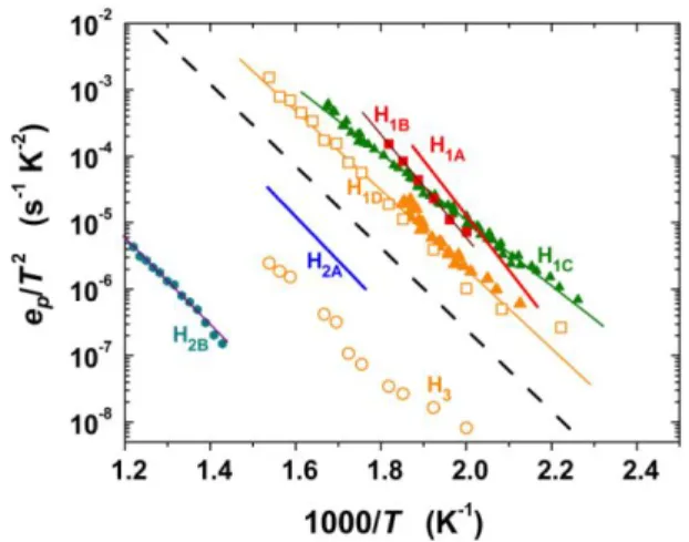
Figure 2 Arrhenius diagram of the various hole traps detected in
this work (symbols and light solid lines) and in references quoted in the text (bold solid lines). Full symbols are derived from FT-ITS technique while open symbols come from high resolution ITS (HR-ITS). The broken line shares the area into two zones comprising: above it, in zone #1, the hole traps labelled H1i (i = A,
B, C, D); below it, in the zone #2, the centres H2A, H2B. The
crite-rion for sorting out the traps in this way will be documented in sections 2.2 and 2.3.
Label Ionisation energy (eV) Capture cross section (cm2) H1A 1.57±0.04 (2-8)1012 H1B 1.57±0.03 (1-2)1011 H1C 0.99±0.04 (2-6)10 17 H1D 1.08±0.05 (4-8)1016 H2A 1.11±0.04 (1-4)1018 H2B 1.33±0.08 (1-4) 1019 Table 1 Hole trap parameters.
It must be stressed that the capture cross sections are not deduced from the intercept of the straight lines drawn in the Arrhenius plot because uncertainties of one to two orders of magnitude can result. Conversely, they are
ad-1 2 3 4 5 6 7 8 9 10 11 12 13 14 15 16 17 18 19 20 21 22 23 24 25 26 27 28 29 30 31 32 33 34 35 36 37 38 39 40 41 42 43 44 45 46 47 48 49 50 51 52 53 54 55 56 57
justed in order that the maxima of the simulated isothermal spectra (or DLTS spectra), calculated with the mean value of the activation energy deduced from the Arrhenius dia-gram (table I), fit the experimental ones, simultaneously at several temperatures (or several frequencies). In this way, the resulting uncertainty upon each capture cross section is considerably reduced, and is tabulated in table I. This pro-cedure is a clear benefit of the quantitative Fourier trans-formation performed on the transients in comparison to standard DLTS which relies only on Arrhenius signatures. The differences in the shape of the spectra appearing in Fig. 1 outside the peak maxima will be discussed further.
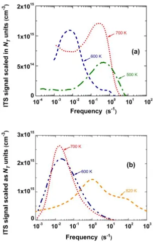
Figure 3 Isothermal spectra, all measured at 500 K, after
sub-sequent annealing temperatures in increasing order, indicated in the figure ; (a) then (b) data have been acquired in this order for two different diodes fabricated on the same sample.
From the capture cross section value, the charge state before hole capture can be guessed for each trap: with very large capture cross sections, equivalent to 7-21 nm for the potential well radius, H1A, H1B are strongly attractive and
therefore negatively charged. So these traps are deep ac-ceptors. Other traps are not attractive for holes before cap-ture and hence either neutral or perhaps even repulsive in the case of H2A and H2B. As it can be seen in Fig. 2 around
the abscissa corresponding to 500 K i.e. (1000/T ) = 2, sev-eral deep levels may contribute together with similar val-ues of the emission rate, although the data have been ac-quired in distinct Schottky diodes fabricated on different samples. Consequently, distributions of emission rates, dif-ferent from a single Dirac-like peak, may occur. The open symbols in Fig. 2 are derived from applying the FTIKREG algorithm [19, 20] to logarithmic transients, a procedure which we call high resolution isothermal spectroscopy (HR-ITS). It is worthwhile to notice that for H1D, the points
coming from FT-ITS (full symbols) are aligned onto those derived from HR-ITS. Conversely, the uncertainties are too large, due to an unfavourable signal to noise ratio, to de-duce valuable parameters for H3.
Complementary properties of the two families of trap can be inferred from other experimental techniques with the purpose of finding indications on the physical origin of the corresponding defects.
3 Metastable properties of the traps H1A, H1B,
H1C, H1D and H3
Several diodes comprising Al Schottky contacts of circular shape with diameters 160 or 200 µm, surrounded by a pla-nar Ti/Pt/Au ohmic contact, initially annealed at 1000 K, are defined by lithography on two samples, the first one doped at 21017 B/cm3, the second one at 21016 B/cm3, both grown in the laboratory of the two last authors. Sub-sequent runs for measuring ITS under the same electrical conditions have been performed after submitting the sam-ples to increasing annealing temperatures.
Figure 4 Concentration of the trap H1C as a function of depth
below the metal-diamond interface.
In order to compare the response of deep traps after each thermal cycle, ITS shown in Fig. 3 have been all ac-quired at 500 K in two diodes of the second sample in the chronological order (a) then (b). It must be stressed that these thermal cycles followed an anneal done at 1000 K, which was performed initially for ensuring ohmicity of the
4 Author, Author, and Author: Short title
Copyright line will be provided by the publisher
1 2 3 4 5 6 7 8 9 10 11 12 13 14 15 16 17 18 19 20 21 22 23 24 25 26 27 28 29 30 31 32 33 34 35 36 37 38 39 40 41 42 43 44 45 46 47 48 49 50 51 52 53 54 55 56 57
Ti/Pt/Au contacts. Moreover, if the spectra at 600 K are quite similar in Fig. 3 (a) and (b), this is no longer true at 700 K. Consequently, the variations of the spectra appear-ing in Fig. 3 are not due only to thermal cycles with maxi-mal temperatures of 500, 600, 700 or 820 K since a previ-ous annealing was made at 1000 K. It is noticeable that the maxima observed in these various spectra are located ei-ther close to 10-2 s-1 or to 1 s-1. When these emission rates are put in the Arrhenius diagram of Fig. 2, they are respec-tively located close to the H3 and H1D lines. Considering
these findings, one is forced to invoke an other physical quantity able to drive changes in the characteristic proper-ties of the hole traps responsible for these spectra. The more obvious influence which can play a role consists in the electric field which is induced by the reverse bias volt-age of either 1 or 2 volts and applied to the diode only during measurements.
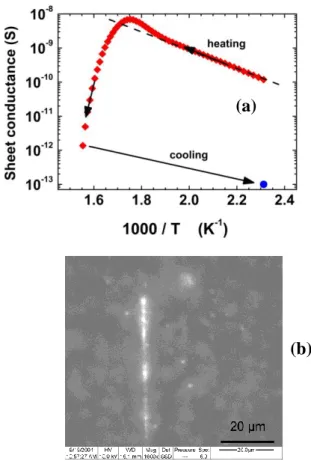
Figure 5 (a) Irreversible evolution of the sheet conductance
upon annealing at 650 K in sample INb, with the simultaneous occurrence of plastic relaxation of strain testified by the CL im-age of the A-band (b), where the lighter the area, the higher the 2.83 eV intensity. Such an image was not possible before the thermal cycle because the 2.83 eV signal was too low everywhere in the sample. At the beginning of heating, the activation energy is 0.48 eV, already above the 0.37 eV expected for Boron accep-tors.
Figure 6 Spontaneous cracks network in undoped sample INc,
9 µm thick, grown on a Ib substrate.
Therefore, charged species, able to migrate under the electric field action, are likely involved in the defects re-sponsible for these hole traps. Moreover, it is known from secondary ion mass spectroscopy (SIMS) performed in CVD homoepitaxial layers that hydrogen may be accumu-lated close to the surface with a decreasing concentration in depth. Concentration profile of trap H1C which gives the
spectrum plotted at 700 K in Fig. 3 (a), is displayed in Fig. 4 and shows also the same trend. All these experimental facts strongly suggest that this family of traps is related to defects incorporating hydrogen atoms. The capture cross sections of H1C and H1D (table I) suggest a neutral state
be-fore hole capture and hence 0/+ states. On the contrary, the unusually high capture cross sections of H1A and H1B,
which are expected for shallow levels, not for deep levels, likeky indicate a spatial agglomeration of defects. Al-though vacancy clusters are specially observed in brown diamond [21], one cannot exclude their existence in CVD layers, mostly because they can be stabilized by hydrogen atoms. Indeed, several authors have observed that the dis-tribution of hydrogen is influenced by trapping defects [22, 23]. Moreover, the concentration profile of H1A shows a
peak near a depth of 200 nm, which broadens after anneal-ing [11]. Clusteranneal-ing of the correspondanneal-ing defects may comply with such a profile. It is also well known that only the positively charged hydrogen atom is able to migrate easily in diamond and that it can occupy various sites [24, 25], thus explaining the observed metastability. But one cannot exclude that BHn centres or complexes correspond
to either H1C or H1D [26], because the traps concentration
detected in the present work is always lower than that of Boron and that negatively charged complexes incorporat-ing hydrogen may be present like suspected in [23].
(b)
(a)
1 2 3 4 5 6 7 8 9 10 11 12 13 14 15 16 17 18 19 20 21 22 23 24 25 26 27 28 29 30 31 32 33 34 35 36 37 38 39 40 41 42 43 44 45 46 47 48 49 50 51 52 53 54 55 56 57
4 Deep donors H2A and H2B
In samples grown in the laboratory which the first six present authors belong to, the hole trap H2A has been
de-tected in conjunction with the onset of the A-band, cen-tered at 2.83 eV in the cathodoluminescence (CL) spec-trum [16], which is considered as being induced by dislo-cations [27,28] or rather defects attached to them [29]. This trap H2A was characterised by a capture cross section in the
10 cm2 range, suggesting either a possible repulsive be-haviour for holes (+/++), or at least 0/+ charge states.. It was also detected in samples coming from the laboratory where the two last authors of ref [11, 16] are affiliated to, with a decreasing concentration inwards the diamond layer. It is expected that such a trap has a compensating activity against boron acceptors. Two new pieces of evidence of such a property are given below, from measurements and images obtained in three samples, INa, INb and INc, grown in the first laboratory.
Figure 7 Conductivity of the INa sample, comprising a
ho-moepitaxial layer grown on a CVD (100) oriented substrate, measured at two locations as indicated by arrows: at left on the as-grown layer, 700 nm thick; at right on the etched layer, 200 nm thick. In the inset, the birefringence image of the substrate is shown.
In the sample INb, simultaneously with the photo-induced current transient spectrum (PICTS) shown in [30], an irreversible decrease in conductivity occurred (Fig. 5a), concurrently with the onset of the A-band illustrated here by a CL image (Fig. 5b) and by CL spectra in ref. [11,30]. Almost complete compensation of Boron acceptors by do-nors H2A happened after the onset of the dislocations.
Plas-tic relaxation of strain arose from the addition of a thermal expansion induced by a temperature gradient to the pre-existing strain coming from the difference between the lat-tice parameter of the Ib substrate and the very lightly doped homoepitaxial layer, containing only about 71014 B/cm3 [18]. Such a plastic relaxation have been found to induce cracks in a similar layer (sample INc), except for its larger thickness of 9 µm (Fig. 6).
Figure 8 PICTS spectra of samples INa and INb at 0.1 Hz after
a 1 s light pulse generated by a deuterium flash lamp.
In sample INa, a homoepitaxial layer 700 nm thick, con-taining 21018 B/cm3, as check by SIMS, was grown on a CVD substrate, containing a very large number of thread-ing dislocations, as shown in the birefrthread-ingence image shown in the inset of Fig. 7. Cathodoluminescence meas-urements confirm the high density of dislocations in the layer with an A-band intensity three time larger than the free exciton one. Circular Schottky and ohmic contacts were deposited both on the top surface of the homoepi-taxial layer and also on the surface of a thinner layer, 200 nm thick, obtained after etching in a microwave electron cyclotron resonance (ECR) plasma of oxygen. No rectify-ing behaviour was observed on the 700 nm thick layer while poor Schottky characteristics were obtained in only 10% of the diodes made on the 200 nm thick layer. Con-ductivity measurements were then possible in non rectify-ing contacts and displayed a high contrast between the two zones (Fig. 8): the thicker layer exhibited the lower con-ductivity by more than three orders of magnitude in com-parison to the thinner layer, which has the expected 300 K conductivity for diamond doped at 21018 B/cm3. Such a fact must be ascribed to a full compensation in the first hundreds nm of the initial layer, which is much less con-ductive, whereas capacitance voltage measurements done in rectifying diodes of the etched layer still indicated a 80% compensation ratio. The deep donors responsible for this compensation are still H2A, as shown by the similar
PICTS spectra found in samples INa and INb (Fig. 8). The small shoulder near 470K in the spectrum measured in INa cannot justify that other deep levels play a significant role. Such an experiment confirms that dislocations are neces-sary for the existence of the H2A donor level, but not
suffi-cient because the density of threading dislocations is not expected to vary with the depth since they are crossing the whole layer whereas the H2A concentration clearly
de-creases inwards the homoepitaxial layer, as already found in the weakly compensated sample of ref. [11].
Hence, it must be concluded that H2A is not only
re-lated to dislocations alone but also to an impurity or an other defect linked to the dislocations. This model agrees
6 Author, Author, and Author: Short title
Copyright line will be provided by the publisher
1 2 3 4 5 6 7 8 9 10 11 12 13 14 15 16 17 18 19 20 21 22 23 24 25 26 27 28 29 30 31 32 33 34 35 36 37 38 39 40 41 42 43 44 45 46 47 48 49 50 51 52 53 54 55 56 57
very well the idea of stable dislocations having only recon-structed dangling bonds and therefore no states in the bandgap [29], but able to capture other defects or impuri-ties. Therefore, an additional impurity or defect must be present for creating an energy level in the bandgap. One more time, the proton may be a good candidate.
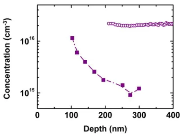
Figure 9 Concentration of shallow acceptors (open circles) and
H2B deep donor levels (full squares) in the second sample
de-scribed in section 3.
In the samples studied in section 3, which are weakly compensated, the H2A level did not appear. However, an
other donor level H2B, with a capture dross section ten
times lower and an ionisation energy slightly larger (see table 1) develops. Its concentration profile is still decreas-ing toward the interior of the homoepitaxial layer, as shown in Fig. 9, and stays below the shallow acceptor con-centration, at least beyond a depth of 100 nm.
5 Conclusions In homoepitaxial diamond layers,
hole traps are studied. They can be sorted out into two sets : (i) deep levels, with ionisation energy either in the range 0.99 eV to 1.15 or at 1.57 eV, the latter with a very high capture cross section (acceptors), ascribed to clusters of defects possibly associated with hydrogen ; (ii) donor levels able to compensate the shallow acceptors in samples comprising a large density of dislocations. The first family shows metastability. In the last case, decreasing concentra-tion profile inwards the layers suggest also that they may be associated to hydrogen. All these deep levels display such attenuation of their concentration beyond some depth, a fact which is fully compatible with the absence of hole traps in pn junctions near 1 µm depth as shown in ref. [31].
Acknowledgements The authors wish to thank B.
Fernandez for his assistance in lithography, the Rhône Alpes Regional Council (France) and the “Agence Nation-ale pour la Recherche” (France) through the contracts “CIBLE 2006”, “DIAMOOND BLAN 06-2-134411” and “DOPEN 06 BLAN 0339-02” for their financial supports.
References
[1] T. Teraji, phys. stat. sol., (a) 203, 3324 (2006).
[2] T. Nakai, K. Arima, O. Maida, T.Ito, J. Crystal Growth 309, 134 (2007).
[3] J. Achard, F. Silva, A. Tallaire, X. Bonin, G. Lombardi, K. Hassouni, A. Gicquel, J. Phys. D: Appl. Phys. 40, 6175 (2007).
[4] V. Mortet, M. Daenen, T. Teraji, A. Lazea, V. Vorlicek, J. D'Haen, K. Haenen, M. D'Olieslaeger, Diamond Relat. Mat.
17, 1330 (2008).
[5] P.-N. Volpe, J. Pernot, P. Muret, F. Omnès, Appl. Phys. Letters 94, 092102 (2009).
[6] P. J. Dean, E. C. Lightowlers, D. R. Wight, Phys. Rev. 140, A352 (1965).
[7] E. A. Konorova, S. A. Schevchenko, Sov. Phys. Semicond.
1, 229 (1967).
[8] L. Reggiani, S. Bosi, C. Canali, F. Nava, S. F. Kozlov, Phys. Rev. B 23, 3050 (1981).
[9] R. Zeisel, C. E. Nebel, and M. Stutzmann, Phys. Rev. B 60, 2476 (1999).
[10] P. Muret, C. Saby, F. Pruvost, and A. Deneuville, Diamond Relat. Mat. 9, 1041 (2000).
[11] P. Muret, J. Pernot, T. Teraji, and T. Ito, Appl. Phys. Ex-press 1, 035003 (2008).
[12] M. Wade, M. Kadri, E. Bustarret, A. Deneuville, P. Muret, C. Araujo, phys. stat. sol. (a) 201, 2457 (2004).
[13] P. N. Volpe, P. Muret, F. Omnès, phys. stat. sol. (a) 205, 2173 (2008).
[14] N. Habka, M.-A. Pinault, C. Mer, F. Jomard, J. Barjon, M. Nesladek, P. Bergonzo, phys. stat. sol. (a) 205, 2169 (2008). [15] P. Muret, C. Saby, F. Pruvost, A. Deneuville, Diamond
Re-lat. Mat. 9, 1041 (2000).
[16] P. Muret, J. Pernot, T. Teraji, T. Ito, phys. stat. sol. (a) 205, 2179 (2008).
[17] S. Weiss, R. Kassing, Solid. St. Electron. 31, 1733 (1988). [18] M. Wade, P. Muret, F. Omnès, A. Deneuville, Diamond
Relat. Mat. 15, 614 (2006).
[19] J. Weese, Comput. Phys. Commun. 69, 99 (1992).
[20] P. Muret, A. Philippe, E. Monroy, E. Munõz, B. Beaumont, F. Omnès, P. Gibart, Mat. Sci. Engineering B 82, 91 (2001). [21] R. Jones, L. S. Hounsome, N. Fujita, S. Öberg, P. R.
Brid-don, phys. stat. sol. (a) 204, 3059 (2007).
[22] Z. Teukam, D. Ballutaud, F. Jomard, J. Chevallier, M. Ber-nard, A. Deneuville, Diamond Relat. Mat. 12, 647 (2003). [23] C. Saguy, C. Cytermann, B. Fizgeer, V. Richter, Y. Avigal,
N. Moriya, R. Kalish, B. Mathieu, A. Deneuville, Diamond Relat. Mat. 12, 623 (2003).
[24] J. P. Goss, R. Jones, M. I. Heggie, C. P. Ewels, P. R. Brid-don, S. Őberg, Phys. Rev. B 65, 115207 (2002).
[25] J. Chevallier, B. Theys, A. Lusson, and C. Grattepain, A. Deneuville and E. Gheeraert, Phys. Rev. B 58, 7966 (1998). [26] J. P. Goss, P. R. Briddon, S. J. Sque, R. Jones, Phys. Rev. B
69, 165215 (2004).
[27] J. Ruan, K. Kobashi, W. J. Choyke, Appl. Phys. Lett.,
60, 3138 (1992).
[28] D. Takeuchi, H. Watanabe, S. Yamanaka, H. Okushi, H. Sawada, H. Ichinose, T. Sekiguchi, and K. Kajimura, Phys. Rev. B, 63, 245328 (2001).
[29] R. Jones, Diamond Relat. Mat., in press (doi:
1 2 3 4 5 6 7 8 9 10 11 12 13 14 15 16 17 18 19 20 21 22 23 24 25 26 27 28 29 30 31 32 33 34 35 36 37 38 39 40 41 42 43 44 45 46 47 48 49 50 51 52 53 54 55 56 57
[30] P. Muret, M. Wade, phys. stat. sol. (a) 203, 3142 (2006). [31] C. Tavares, P. Muret, S. Koizumi, F. Jomard, phys. stat. sol.