HAL Id: tel-01340397
https://tel.archives-ouvertes.fr/tel-01340397
Submitted on 1 Jul 2016HAL is a multi-disciplinary open access archive for the deposit and dissemination of sci-entific research documents, whether they are pub-lished or not. The documents may come from teaching and research institutions in France or abroad, or from public or private research centers.
L’archive ouverte pluridisciplinaire HAL, est destinée au dépôt et à la diffusion de documents scientifiques de niveau recherche, publiés ou non, émanant des établissements d’enseignement et de recherche français ou étrangers, des laboratoires publics ou privés.
Multi-engine multi-level simulation for system
specification validation and power consumption
optimization
Fangyan Li
To cite this version:
Fangyan Li. Multi-engine multi-level simulation for system specification validation and power consumption optimization. Other. Université Nice Sophia Antipolis, 2016. English. �NNT : 2016NICE4008�. �tel-01340397�
UNIVERSITE NICE SOPHIA ANTIPOLIS
POLYTECH’NICE-SOPHIA
École Doctorale des Sciences et Technologies de
l’Information et de la Communication
Electronique pour Objets Connectés
THESE
Pour obtenir le titre de
Docteur en Sciences spécialité Electronique de l’Université Nice Sophia Antipolis
présentée et soutenue par
Fangyan LI
Simulation multi-moteurs multi-niveaux pour la validation
des spécifications système et optimisation de la consommation
Thèse dirigée par Gilles JACQUEMOD Soutenance le 29 Mars 2016 Jury :
Y. DEVAL Rapporteur Professeur, IPB Bordeaux I. O’CONNOR Rapporteur Professeur, Ecole Centrale Lyon G. JACQUEMOD Directeur Professeur, UNS Sophia Antipolis
E. DEKNEUVEL Encadrant MCF, UNS Sophia Antipolis
R. BUTAUD Examinateur Ingénieur, Riviera Waves Sophia Antipolis F. PECHEUX Examinateur Professeur, UPMC Paris
Avant
‐propos
Le travail présenté dans ce mémoire a été effectué au sein du Laboratoire EpOC, URE UNS 006, et cofinancé par la société Riviera Waves (convention Cifre). Il s’inscrit dans le cadre du projet CoCoE, soutenu par la Plateforme Conception CIM‐PACA. Je tenais à remercier …….
Table
des Matières
Introduction ... 3 1. Motivation ... 3 2. Context ... 4 3. Thesis organization ... 5 Chapter I – Mixed signal modelling for BT communication ... 7 1. Introduction ... 7 2. Methodology ... 8 2.1. Mixed signal design methodology ... 8 2.2. Baseband equivalent modelling ... 11 2.3. Analog/RF front‐end architectures ... 12 2.3.1. Heterodyne receiver ... 12 2.3.2. Homodyne (or zero‐IF) receiver ... 13 2.3.3. Low‐IF (or pseudo zero‐IF) receiver ... 13 2.4. Analog/RF blocks modelling considerations using the MIM approach ... 14 2.4.1. Noise modelling ... 14 2.4.2. Phase noise ... 16 2.4.3. Non‐linearity ... 18 2.4.4. Average power ... 24 2.4.5. Conclusion ... 24 3. Bluetooth Low Energy standard ... 24 3.1. Introduction ... 24 3.2. BlueTooth and BLE ... 25 3.3. BLE system architecture ... 25 3.4. BlueTooth and BLE link layer ... 26 3.4.1. LL states ... 27 3.4.2. BLE Packet format ... 27 3.4.3. LL state machine operations ... 28 3.5. BLE Physical layer description ... 31 3.6. GFSK modulation ... 32 3.7. Direct and indirect angle modulation ... 33 4. SystemC toolset : Mixed signal simulation tools ... 33 4.1. Introduction ... 33 4.2. SystemC ... 34 4.3. SystemC‐AMS ... 34 4.4. Verilog‐AMS, VHDL‐AMS ... 34 4.5. Matlab ... 35 4.6. Mixing SystemC MoCs... 35 4.7. Conclusion ... 365. Conclusion ... 37 Chapter II – BLE transceiver modelling ... 39 1. Introduction ... 39 2. Transceiver modelling and simulation ... 40 2.1. GFSK modulation modelling ... 40 2.1.1. GFSK modulator architecture ... 40 2.1.2. Bits generator ... 41 2.1.3. Gaussian filter ... 42 2.1.4. Digital integrator ... 43 2.2. Demodulator modelling ... 44 2.2.1. Demodulator architecture ... 44 2.2.2. Arctangent operation and derivation ... 44 2.2.3. Correlator ... 45 2.3. Analog/RF Tx modelling ... 46 2.3.1. Tx architecture ... 46 2.3.2. Digital‐to‐Analog convertor ... 46 2.3.3. Low pass filter modelling ... 46 2.3.4. RF conversion ... 47 2.4. Analog/RF Rx functional modelling... 48 2.4.1. Rx architecture ... 48 2.4.2. Low‐IF down‐conversion at ‐1MHz ... 48 2.4.3. Complex transfer function modelling ... 49 2.4.4. Sigma‐Delta ADC ... 51 2.5. Receiver digital BB modelling ... 52 2.5.1. Rx BB architecture ... 52 2.5.2. Low pass filters ... 53 2.5.3. CXF2 modelling ... 54 2.5.4. 4‐tap filters ... 55 2.5.5. Down‐sampling of 4 and frequency shifting ... 56 2.6. Transceiver functional model simulation ... 56 3. Simulation time optimization ... 57 4. Rx front‐end refinement with RF specifications ... 58 4.1. RF channel model ... 59 4.2. Receiver analog block refinement method ... 59 4.3. Refinements of Rx analog/RF blocks ... 60 4.3.1. LNA refined model verification ... 61 4.3.2. Mixer refined model verification ... 62 4.3.3. Analog complex filter refined model verification ... 64 4.3.4. ADC modelling, verification and characterization ... 65 4.4. Cascaded specifications verification ... 65 4.4.1. Rx front‐end NF simulation ... 66
4.4.2. Rx front‐end IP3 simulation ... 66 4.5. PLL phase noise ... 67 5. Transceiver simulation and BER estimation ... 68 6. Conclusion ... 69 Chapter III – System modelling and simulation ... 71 1. Introduction ... 71 2. Parametrized receiver blocks ... 72 2.1. Introduction ... 72 2.2. Parametrized LNA ... 72 2.3. Parametrized analog filters ... 72 2.4. Digital filtering (ADC and D‐filters) ... 73 3. SCTLM platform at LL level and PHY interface ... 75 3.1. Introduction ... 75 3.2. Passive scan thread ... 76 3.3. Air Modelling ... 77 3.4. Interface creation between LL and transceiver ... 78 3.4.1. Data path ... 78 3.4.2. Control path ... 80 3.5. Transceiver configuration and integration in TLM system ... 83 3.6. Global simulation of BLE system ... 84 3.6.1. Introduction ... 84 3.6.2. Simulation platform construction ... 84 3.6.3. BLE use cases and Energy estimation ... 85 3.6.4. Simulation and energy consumption results ... 86 3.7. Example of application: optimization of the transceiver energy consumption ... 88 3.7.1. RF system optimization ... 88 3.7.2. RF chain with new configuration example ... 89 3.7.3. Simulated results ... 90 3.8. Conclusion ... 91 4. WSN modelling and simulation ... 92 4.1. Introduction ... 92 4.2. Network‐level modelling ... 93 4.3. Model abstraction ... 94 4.4. Simulation results ... 96 5. Conclusion ... 97 Conclusion and Trends ... 99 1. General conclusion ... 99 2. Perspectives ... 100 Publications ... 101 References ... 103 Annexe : Résumé étendu en français ... 105
Acronym
AA Access Address
ADC Analog to Digital Converter AGC Automatic Gain Control AMS Analog and Mixed Signal AWGN Additive White Gaussian Noise
BB and BBE Base Band and Base Band Equivalent model BER Bit Error Rate
BT and BLE BlueTooth and Bluetooth Low Energy CoCoE Contrôle de la Consommation Electrique CRC Cyclic Redundancy Check
DAC Digital to Analog Converter
DSP Digital Signal Processor (or Processing) EDA Electronic Design Automation
ELN Electrical Linear Network FIR Finite Impluse Response filter GF Gaussian Filter
GFSK Gaussian Frequency Shift Keying IFT Inverse Fourier Transform IoT Internet of Things
ISM Industrial, Scientific and Medical band LNA Low Noise Amplifier
LPF Low Pass Filter
LSF Linear Signal Flow
LTF Laplace Transfer Function
LL Link Layer
MAC Medium Access Control MIM Meet‐In‐the‐Middle MoC Model of Computation
NF Noise Figure
PDU Protocol Data Unit PSD Power Spectrum Density
RMS Root Mean Square
RTL Register Transfer Level
SCAMS SystemC‐AMS (Analog Mixed Signal)
SCTLM SystemC‐TLM (Transaction Level Modelling) SCNSL SystemC Network Simulation Library SNR Signal to Noise Ratio TDF Timed Data Flow TLM Transaction Level Modelling
Introduction
1.
Motivation
For several decades, the communicating objects invaded our everyday life and the number of transmitted data, associated with numerous standards of wireless communication, also exploded. Nowadays, objects are connected each other’s, without sometimes human intervention, and connected to Internet; we speak then about Internet of Things (IOT). Many IOT applications require communicating wireless objects powered by autonomous battery for (mobility and easy to install) low cost and long autonomy (small reloadable battery, energy harvesting, low power consumption) systems. The transmission of a small quantity of data with regular interval of a large number of objects towards Internet imposes the use of a fixe (home, public places, etc.) or mobile (smartphone) gateway. The radio communication standards adapted to these applications are for example Bluetooth Low Energy (BLE) [1], ANT+ [2], or ZigBee [3].
In conclusion, the large-scale deployment of the internet of things generally and wireless sensors' networks in particular, requires the development of electronic circuits and systems more and more energy-efficient. Reducing the bill of materials and time-to-market can best be achieved through the broadest and most complete integration, one that also includes elements such as the antenna and/or the packaging where system-in-package (SiP) technologies are involved. It is clear that preparing them to handle the different signal shapes and frequencies is no trivial task. Indeed, during different design phases, engineers have to account for such factors as bit error rate (BER) on one hand, and power consumption on the other. Block design requires that electrical properties are set with due consideration for factors such as noise, nonlinearity, gain or impedance matching. Each step requires different simulators, and all must be interoperable. Even then, there is usually a design gap between the system specification and the RF block design. It typically centers on:
the use of different design frameworks and different simulators;
a huge frequency ratio between the RF (GHz) and the digital baseband (MHz).
Nevertheless, to meet an original system-level specification, engineers need to mix different levels of abstraction so that they can explore implementation architectures and then validate the final design at the circuit level. Luckily, existing behavioral models in the SystemC-AMS (or VHDL-AMS) analog and mixed signal language provide the basis for such a seamless system-to-transistor-level approach. Relevant features include:
top-level functional simulations for architecture validation using a top-down methodology;
bottom-up verification with accurately characterized models;
test program development using tester resource models;
traditional measurement, post-processing and/or the use of testbenches;
IP exchange and protection to help assess a model against a specification.
This thesis proceeds from the position that designing such complex systems requires the development of a single EDA framework composed of multi-engine simulators that are associated with a library of hierarchical models. We have illustrated this approach in the domain of wireless remote sensors using BLE (Bluetooth Low Energy) standard for smart building application.
2.
Context
This research belongs to the CoCoE project (Contrôle de la Consommation Electrique dans les bâtiments) of ARCSIS (Pôle de compétitivité Solutions Communicantes Sécurisées) and CIM-PACA Design Platform. Partners of this project are EpOC (URE UNS 006) and IM2NP (UMR AMU-CNRS 7234) laboratories, Qualisteo and RivieraWaves companies. The objective of this project is to develop an innovative, non-intrusive and communicating solution for electrical energy measurement in the building. Today, optimizing energy in building is based on the total electrical power consumption, with no detailed information about power consumed in individual appliances. Thus, solution so far needs complex systems with many meter and sensors, which is incompatible and inconvenient with existing building.
The problematics, which must be solved by the CoCoE project, are that the electric power consumption information is less accessible, not in real-time without any information about kind of appliances and usage, even with the Linky future smart meter. This can be solved by using NIALM (Non-Intrusive Appliance Load Monitoring) technology implemented into FPGA and with the development of remote wireless sensors. There are two other PhD students working on this project in developing these new sensors to measure electrical current [4] and new NIALM algorithms with FPGA implementation [5] (Cifre Thesis with Qualisteo Company). The aim of this work, in collaboration with Riviera Waves Company (Cifre Thesis) is to model and optimize wireless communication systems (BlueTooth Low Energy, BLE standard) using SystemC-AMS language. This standard, BLE, will be used to interconnect the wireless current sensors in a building for appliance monitoring. The CoCoE project received an award during the World Efficiency Congress (Paris, October 2015): “Lauréat du Trophée de la Recherche Publique Energie-Climat-Environnement”, given by ADEME and the two magazines EnergiePlus and Mesures, in the topic of Energy efficiency. Moreover, CoCoE is a building block of the “Smart Campus Nice Sophia Antipolis” project, which has been labeled by the French ministry of industry on the national industrial plan on smart grid.
3.
Thesis organization
The report of this thesis, besides an introduction and a general conclusion, includes three chapters:
Chapter I: Mixed signal modelling for BT communication. This chapter presents the description methodologies of the heterogeneous systems: top-down approach, Bottom-Up approach and meet-in-the-middle approach. Then, we remind the various RF front-end, as well as the different characteristics of RF segments and their modelling in Base Band (BB) equivalent circuit. We focus on the BT and BLE standard. To conclude this chapter, we show how the SystemC and SystemC-AMS languages can describe the different parts of a BLE transceiver.
- Chapter II: BLE transceiver modelling. In this chapter, we describe the different building blocks of a BLE transceiver. We remind the principle of the GFSK modulation to describe the block of bits generation. Thanks to the Riviera Waves Company design, a Zero-IF topology is chosen for the RF transmitter and a Low-IF for the RF receiver. Firstly, the “ideal” building blocks are described from a functional point of view and validated by simulations (integrator, correlator, modulator, filters, converter, … : in different domains: digital, analog and RF). Because of the prohibitive simulation time, the RF blocks are rewritten by using the BB methodology and then, refined to take into account the non-idealities which are going to impact on the couple consumption, BER. Every circuit (every model) is separately validated. Then a first system simulation (point to point communication between a transmitter and a receiver) is made. Finally the BER is estimated with suitable simulation time and the results were validated from measures on a circuit designed by the Riviera Waves Company.
- Chapter III: System modelling and simulation. This chapter is dedicated to the simulation of a real use case given by the Riviera Waves Company in order to verify the functioning of the system and to estimate the power consumption for a given use case. Several use cases are analyzed and compared. Finally, two versions of a same architecture are modelled, simulated and compared. The results show that the new version allows to increase the global performances of the system, in term of BER and power consumption. To conclude this chapter, we show that it was possible to reuse our models for a higher level simulation (sensors' network) by integrating them into the SCNSL platform, developed by the University of Verona to Italy, with whom we collaborated.
Chapter
I – Mixed signal modelling for
BT
communication
1.
Introduction
The design of wireless systems is becoming increasingly complex because of the great number of functional requirements for the application and non-functional constraints such as maximum energy consumption and minimum dependability. Simulation is strongly needed to verify that specifications are met and the simulation of communication aspects is crucial for the verification of today’s wireless systems [6].
Figure 1.1 shows an example of a 2 nodes wireless communication system [7]. A complete wireless system like this can be divided into three different domains as: Digital Signal Processing (DSP), Analog BaseBand (BB) and Radio Frequency (RF) transceiver, according to the three different types of signal (mixed -digital and analog- and RF signal).
Fig. 1.1: Different domains of a 2 nodes wireless communication system and signals characteristics
A communication task involves all these parts but usually their behavior is simulated by using different tools and different models of computations. Hardware description languages (e.g., VHDL, Verilog, SystemC) are used for the whole architecture modelling and for the digital baseband (BB) block. Data flow simulators (e.g., Matlab/Simulink and SystemC-AMS) are used for optimization of signal processing algorithms, frequency planning, noise budget, bit error rate (BER) and power optimization. Specifically, there is a gap between system level and RF block simulation. RF circuit and communication channel handle radio waves and belong to continuous-time domain. The other components are digital and described by using discrete-time models of computation. Therefore, we need some techniques to handle heterogeneity.
Furthermore, the communication task consists of several aspects which cannot be simulated all together because of the huge different simulation time scale between domains. So we need to find out suitable compromises to be able to simulate different domains while keeping the accuracy of the specifications of interest.
In this chapter, we will first give a brief introduction about the problems of wireless mixed system modeling. In the next subsection, the methodologies focus on the problems solving and modeling considerations are talked, which involve: the system modeling approach and techniques choosing, introduction of different receiver types and the common RF circuit specifications considerations. The Bluetooth Low Energy standard will be presented in the third subsection with a focus on the Link Layer level and the Physical level. Briefly introductions of the common used tools and languages for mixed signal modeling and the chosen ones for this work are presented in the fourth subsection. And finally is a conclusion about this chapter.
2.
Methodology
2.1.
Mixed signal design methodology
Methodologies for the mixed design of wireless sensors network can be resumed as below, and illustrated by Figure 1.2. This approach uses a four-level hierarchical model library: transistor (SPICE or physical level), structural (low level), behavioral (intermediate) and high level (ESL or specification) [7]. It is also tailored to the three main types of design process: bottom-up, top-down and meet-in-the-middle [8]. The overarching goal is to define the primitive components and objects, and to then develop them and the system structure simultaneously, so that the final system is constructed from these primitives in the middle of the design process. The same paradigm is used to develop the hierarchical models.
The Top-Down approach is based on a design which begins with high level specifications. It is usually used for high level analysis and simulation based on logical and/ or behavioral models that take into account the system requirements.
This approach identifies the main objects of the system by analysis and successive refinements. The high level constraints can be associated to the objects (execution delay, consumption, packaging …). Thanks to the high level and logical models, the simulation time is greatly reduced which makes the architectural exploration easier.
The Bottom-Up approach can be viewed as an exploration of libraries containing models of physical solutions in order to build an architecture (virtual prototype) able to meet all the requirements, which guarantees the practicability of the system. But the complexity of the models increases the simulation time which is not convenient for architectural exploration.
The Meet-in-the-Middle (MIM) approach is based on the use of the lower level model outputs. It aims to extract more accurate performances from lower level design to enrich the higher level simulation. Generic parameters of high level models are extracted from low level simulation. The result of this operation is that we can obtain the accurate enough simulation results of system performances that we are interested in without executing lower level simulation. As the high level and low level are relative to each other, this method allows a flexible refinement or optimization between the lower levels and the higher levels.
Fig. 1.2: Methodology for communicating object modelling
Example of the MIM approach
Figure 1.3 shows an example of a simplified open system interconnection (OSI) model which includes the highest “Upper levels” (higher than network level). Physical level is the lowest level in the OSI architecture. At the physical level, we find various building blocks, such as MODEM and analog/RF transceiver. At this level, the possible performances analyses are the transceiver Bit-Error-Rate (BER) and the power consumption. However, to be able to obtain a BER with the analog/RF component considerations, we need to extract the specifications of lower level analog circuits as the linear gain, noise figure (NF), non-linearity and the block average power.
In Fig. 1.3, the possible extracted performances of each abstraction level are written in a cloud symbol. They can be next used to interface with the higher level models to accelerate the global simulation. Several performances like the physical level BER can be used in all higher levels to perform as the error generator which is also a very important parameter for high level models. We can use the extracted specifications from different lower levels to
enrich different higher levels to realize the simulation we want. It reflects the flexibility of the MIM method.
Fig. 1.3: Simplified OSI model with MIM method
The MIM method itself can not satisfy the physical level modeling due to the capability of modelling the RF blocks at system level. We traditionally over sample the signals by using a simulation frequency dozens of times of the highest signal frequency to keep the RF signal accuracy, which makes the simulation time very long and it is still not possible to co-simulate with Datalink and higher level system.
Limitations of the methodology
The main limitation concerns the development of the hierarchical library. Model development is difficult and needs a high level of expertise to be carried out effectively. Achieving an accurate RF implementation demands the full consideration of such factors as non-linearity effects, compression, noise, phase noise, frequency response, mismatch and so on. Moreover, RF designers also often use proprietary models during simulation, and this often means that there are limited opportunities for their reuse across different design environments.
Increased digital signal processing (DSP) lowers the quality of analog signal processing. Luckily, mixed-signal simulation is now a mature technology, and several unified simulators and co-simulation solutions are available [9]. This smoothes our path to the objective that, wherever possible, one should reuse existing models and unify various platforms in ways that are transparent to the user. The key factors for success are:
- the ability to take a hybrid approach to the integration of different tools; - the use of open databases using standard languages;
In this work, we use a combination of the MIM method and the Baseband Equivalent modeling method, which will be introduced in the next subsection, to realize a global system simulation with a suitable simulation time and it will give system performances with circuit level accuracy.
2.2.
Baseband equivalent modelling
As we know that RF signal simulations, with the conventional oversampling method, require a very high oversampling rate to keep the RF signal accuracy. For example, a BLE RF signal is sent onto the 2.4GHz ISM band. To realize a simulation around 2.4GHz, the simulation frequency should attain 40 to 50 GHz, which makes the simulation out of the computer capacity or the tolerance in simulation time. In terms of narrow band communications like BT/BLE, since the useful in band information occupies very little part in the spectrum, this method waste most of the work on representing the out of band information.
The method of baseband equivalent modeling proposes to suppress the carrier frequency in order to accelerate the simulation speed without losing the RF/analog behavior. This method requires that the RF signal to be narrow band and the equivalent BB model should still be able to perform the RF non-idealities like the non-linearity. The principle of this method is briefly given below.
The principle of the modulation told us that we use the baseband information to vary the three elements, which are the amplitude, the frequency and the phase, of a sinusoidal wave, thus we can obtain the amplitude, frequency or phase modulated signal respectively. An RF modulated signal can be generally represented by the equation below regardless the modulation type we use.
∆ (Eq.1) This equation can be written as
(Eq.2) where represents the total instantaneous phase deviation ∆ . The carrier can be suppressed in the form of Eq.2 as:
(Eq.3) (Eq.4)
The effect of the baseband equivalent modeling method in frequency domain is shown in Figure 1.4.
Fig. 1.4: Baseband equivalent modeling approach
In this case, baseband equivalent signal has to be modeled as a complex signal with two quadrature scalar components I and Q instead of one real signal as .
Once these principles were put, we remind, during this chapter, the receivers' main architectures RF as well as the characteristics (parameters and equations).
2.3.
Analog/RF front‐end architectures
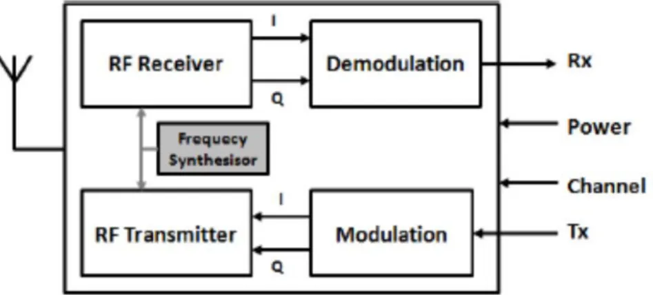
Architectures of a receiver can be divided into the digital and analog/RF parts and interfaced through an analog-to-digital converter (ADC). The analog/RF part in receiver is used to detect and receive the RF signal and convert it to baseband. It should be able to combat the interference and to have enough dynamic range. In this subsection, the different types of RF front-ends are introduced [10].
2.3.1.
Heterodyne
receiver
The architecture of heterodyne receiver, depicted in Figure 1.5, uses an intermediate frequency (IF) before to download the signal in the baseband spectrum.
Fig.1.5: Heterodyne receiver block diagram
After the LNA, the RF signal is filtered by an image rejection (IR) filter to attenuate the image frequency, and then it is down converted to a first intermediate frequency (IF) I⑤ by
mixing an LO of f where is the RF signal carrier frequency or the channel frequency. This IF signal is next filtered by a high selectivity band-pass filter and then down-converted to the baseband by using a quadrature mixer. An ADC is used lastly for the signal digitizing. In comparing with the zero-IF, this architecture avoids the problems like LO leakage and flicker noise but with tradeoff of the complexity. Since it contains complicate filters and two mixing stages, it makes the design expensive and difficult to be integrated.
2.3.2.
Homodyne
(or zero‐IF) receiver
Homodyne receiver, also called zero-IF receiver, has an architecture shown in Fig. 1.6. As other type of receivers, at the input of reception, we use a low-noise amplifier as the first reception block to pull down the chain noise figure (NF). Then it directly convert the desired RF signal down to the baseband with an LO which has the same RF frequency than signal carrier frequency. As the architecture is simple, this kind of receiver is easy to design and to be integrated. However, it suffers from the LO leakage, even-order distortion and the flicker noise.
Fig. 1.6: Direct-conversion receiver block diagram
2.3.3.
Low
‐IF (or pseudo zero‐IF) receiver
The low-IF receiver, which has an architecture shown in the Fig.1.7, aims to avoid these problems by using an LO frequency shift a little bit from the carrier frequency of the received RF signal. The disadvantage of this architecture is that the ADC dynamic range has to be larger than in the zero-IF receiver.
2.4.
Analog/RF blocks modelling considerations using
the MIM approach
To construct system-level models for RF circuits, we need to extract the useful information from low-level RF models or circuits and ignore other low-level details. In this part, we will talk about the mainly considered parameters in RF designs. It is necessary to understand the principle of them to use them lately in the system-level model refinements.
2.4.1.
Noise
modelling
Thermal noise
An additive noise n(t) is often introduced in communication system simulation to analyze the transceiver performances, as shown in Figure 1.8. We can use the PSD (Power Spectrum Density in W/Hz) for the analysis of Eb/N0 or the power (W) for the SNR studying. This noise called additive white Gaussian noise (AWGN) has a normal distribution in the time domain with an average value of zero.
Fig. 1.8: AWGN model
AWGN is normally used to describe noises having Gaussian distribution like thermal noise. But in this work, we use an AWGN source to represent the general noise of an analog RF circuit. This noise is an abstraction of all kinds of the circuit internal noise and it is a method to measure the noisy level of a circuit. In the modeling stage, this value can be used to model the circuit noise as a thermal noise of the block equivalent input impedance to realize the block noise refinement.
Fig. 1.9: Thermal noise of a resistance in tension
The thermal noise is dependent on the temperature, as shown below. For example, in Figure 1.9, a single passive resistor R generates an RMS noise voltage equal to
where k=1.38×10⁻²³ J/K is Boltzmann’s constant, T is the temperature in Kelvin, R is the value of the resistor in Ohms, and B is the bandwidth in Hertz.
Noise Figure and Sensitivity
The noise figure (NF) is an important analog/RF specification. It is used to quantify the impact of the thermal noise in communication systems. NF is defined as the noise factor (F) in decibels, and F is defined as the ratio between the input SNRin (Signal to Noise Ratio) to the output SNRout of an RF block:
(Eq.6) The noise factor, F, of an RF block is always greater than one (zero in decibels) because there is always intrinsic noise in the block and the SNR of this block will be reduced. If we are up to a view of an RF system which is composed of cascaded blocks (cf. Figure 1.10), a receiver front-end composed by a low noise amplifier (LNA), a mixer, an analog filter and an ADC, the total noise factor can be obtained by using the Friis equation:
⋯
… (Eq.7)
where Fn and Gn are the noise figure and the gain of the nth stage respectively
Fig. 1.10: Cascaded noisy blocks
From Eq.7, we can understand that the first stage of a receiver requires a very low noise figure and a high gain in order to obtain a good noise factor of a cascaded system.
The sensitivity is the minimum signal input level required for a specified output SNR of a receiver. The sensitivity of a receiver can be obtained from the required minimum SNRo over the bandwidth B:
SNR and the sensitivity with an integrated thermal noise is obtained as:
Sensitivity ⑤ KT① SNR (Eq.8) It is expressed in dBm with the assumption of the temperature of 290 K:
Sensitivity log ① lg ⑤ log SNR (Eq.9)
AWGN in Simulation
Normally, AWGN can be generated by using a function with the RMS value equals to one. The function gives a series of pseudorandom numbers. In our simulation, AWGN is used to represent a white noise in the whole simulation band which is specified by the simulation sampling frequency fs. This noise should adapt the required noise quantity in the band of interest B.
The AWGN in a simulation is evenly distributed over all the simulation band / . If we consider the noise in voltage, the RMS value of this noise v integrated in the band of interest B can be calculated with the defined block noise figure. For the simulation with a simulation frequency of f , we have to generate an RMS value equal to:
_ /√ (Eq.10) where is the real RMS noise voltage density in /√ , B is the system bandwidth, and is the simulation sampling frequency (cf. Figure 1.11).
Fig. 1.11: Noise voltage density in simulation
In the classical case of thermal noise power that one encounters in many references for simulating the performance of a matched receiver as a function of the SNR or / , we have to generate an AWGN with a power equal to
_ _ (Eq.11) which gives an RMS noise voltage at receiver input of
_ (Eq.12) where R is the receiver input impedance.
2.4.2.
Phase
noise
In RF transceivers the complex baseband signal containing the useful information will be up-converted in the transmitter or down-converted in the receiver by using RF mixers and LO output carriers. If the carriers are ideal, the mixer output signal y t can be written with a complex x t as::
④q.
This mixer output can be written as below with the LO phase noise θ(t):
The phase noise θ(t) is normally described by its PSD in dBc/Hz in the frequency domain. It is defined by the ratio between the noise power measured in 1 Hz bandwidth at a frequency offset f∆ and the power of the carrier. The ideal oscillator is described by a sinusoidal output (in time domain) and is represented by a Dirac function in the frequency domain. Noises, such as flicker and thermal noise, generate a phase noise (in dBc/Hz@f) in
the spectrum of a real oscillator output as described in Figure 1.12.
Fig. 1.12: Oscillator phase noise PLL Phase Noise Modeling in time domain
In analog/RF design the PLL performances are generally defined by their output phase noise profile. PLL phase noise can be well specified by system designers using the model depicted in Figure 1.13.
Fig. 1.13: Phase noise profile in dBc/Hz
In this work, we model a complete PLL phase noise in the frequency domain by using the method presented in [6] as :
∆
∆ ∆ (Eq.15) in which ∆ is the frequency offset from the carrier, is the PLL −3dB bandwidth, and is the in-band phase noise level in / .
This phase noise model can be seen as a low-pass filter for the BB modeling or a band-pass filter for RF modeling by shifting the zero value of ∆ to . We just need to convert this
model to a phase error source by using the Inverse Fourier Transform (IFT), then add it to the LO carriers, as shown in Figure 1.14.
Fig. 1.14: Phase noise temporal simulation model
2.4.3.
Non
‐linearity
When an analog/RF block is nonlinear, its input and output have a relationship approximated by
⋯ (Eq.16) where is the input and is the output. If the input is a single tone of sinusoidal signal as Acosωt, it will lead an output as
Acosωt A cos ωt A cos ⋯
A cosωt cos ωt cos ωt (Eq.17) Where the first term is a dc offset, the second term is the fundamental wave, and the other high order signals are called nth-order harmonics which are integer multiples of the input frequency [11].
This result shows that a nonlinear circuit can generate other frequency components in the output with a single frequency input. We will next talk about several phenomena due to this property and the corresponding RF design specifications.
Gain compression
From Eq.17 we can see that the gain of the desired frequency is
(Eq.18) and when the input amplitude A is very small, the other terms can be ignored since they all contains high order of A, then the output can be approximated as the input multiplied with the fundamental linear factor 1. But as A becomes larger, the term / becomes important
different systems, the factor symbol of the different harmonics could be opposite. Fig. 1.15 (a) and (b) give respectively the development of the output gain of the fundamental signal according to the input amplitude with inphase and and inverted and . Fig.1.15 (c) is the zoom of the common zone of them which indicates that the output can be seen as linear when A is small, but when A keeps arising, the output gain will be compressed.
Fig. 1.15: Gain compression with: (a) inphase and , (b) inverted and , and (c) definition of 1-dB compression point
In RF design, this effect is measured by the specification of “-1dB compression point” (1dB CP) which defines the input amplitude , which corresponds to a nonlinear output point of 1dB less than its ideal linear output as shown in Fig.1.15 (c) and Eq.19.
log , log| | ,
, . (Eq.19)
In the situation of two tones at the nonlinear block input as A cosω t A ω t, the fundamental output signal becomes
A A ⋯ (Eq.20) Cross-modulation
If A ω t is the desired signal and A ω t is an interferer, and A is much strong than A , then the gain of the desired signal in Eq.20 is approximated by . In the case of 1 and 3 are with reversed phase, the gain will be reduced rapidly until zero which is
described as the desired signal is blocked and the interferer is called a blocker (cf. Fig. 1.16).
Intermodulation
Consider still two tones at the input as A cosω t A ω t, the nonlinear output becomes:
A cosω t A ω t A cosω t A ω t ⋯
A cosω t A ω t ⋯
cos cos ⋯ ④q.
We notice that the last two terms exhibit frequencies that do not belong to any harmonic of 1 or 2. We call this phenomenon as Intermodulation (IM). Among the IM products, the
3rd-order IM (IM3) products cos and cos are
very important. If and are adjacent channels, the IM3 at and are adjacent with and respectively (cf. Fig.17 (a)).
In the case that two strong interferers exist at and while the desired signal is transmitting around or , the two IM3 products will drop exactly into the band of interest at the output of the nonlinear block (cf. Fig.1.17 (b)). They increase rapidly as the input interferer amplitudes A1 and A2 increase and finally they will have the same strength
as the fundamentals.
Fig. 1.17: (a) Two-tone intermodulation and (b) example of signal corruption due to IM3 In RF design, we use the 3rd intercept point (IP3) to measure the IM3 products. As shown in Figures 1.18 and 1.19, the IP3 is measured using dual tone input signal. We apply a two tones test with two signals which have the same amplitude A, and draw the linear fundamental amplitude 1A and IM3 amplitudes in a log-log scale with the development of
Fig. 1.18: IP3 definition
Fig. 1.19: IP3 measurement with two-tone test The two curves will cross at a virtual point when:
| | , (Eq.22) where is the input IP3 and the vertical-axis projection is the output IP3. As the actual output curves of the fundamental and IM3 are compressed (continuous lines in Figure 1.18), the IP3 doesn’t actually exist. The measurement should be carried out with very small A which is located in the linear zone. Since the IP3 is normally far away, it is not easy to choose the input amplitude values and the intervals of the iterations. A little offset of the line slope leads to enormous deviation of IP3 values.
Another easier method is based on a hypothesis that the IM3 product equals to the fundamental output when the input reaches . If we applicate a smaller input Ain, it will
generate a fundamental with an amplitude which is log log lower than Aoip3 since the fundamental curve slope in log is 1. This Ain will generate IM amplitude AIM
which is log log lower than . We let the difference between the fundamental output amplitude Aof and the IM product amplitude is ∆ , given by Eq. 23.
∆ log log log log ,
log ∆ log (Eq.23) This method is much more intuitive and easier to applicate but still with cautions that input amplitude should be far away from . This is easy to verify during the IP3 measurement. We only have to overlap the nonlinear output (Eq.21) with a hypothetic linear fundamental output coming from the input multiplied with . The measurement result will be correct only if the fundamental tones superposed which indicates that the input amplitude is small enough to ignore the high order terms in Eq.21, and the output is in the linear zone, as shown in Figure 1.20.
Fig. 1.20: ∆P measurement with situation: (a) correct and (b) wrong Cascaded IIP3
At the end of the nonlinearity measurement introduction, we give a brief conclusion about the cascaded IIP3 measurement.
Fig. 1.21: Cascaded nonlinear blocks
Consider a chain of nonlinear blocks as shown in Figure 1.21. Each block has a measured A , which has a relationship with the chain Aip3 as
, , , ⋯ . (Eq.24) This result also comes from a two tones analysis.
Non-linear modelling using equivalent BB model
We have introduced BB equivalent model in section 2.2. However two problems needed to be solved: How to propagate nonlinear effect between RF components, which cause harmonics in addition to the principal modulated signal? And how to manage adjacent frequencies, a problem met when simulating frequency offset or IIP3 test. To solve the first
problem, Vasilevski [12] proposed to represent a modulated signal more accurately taking into the DC and 2 harmonics into account, as described in Equation 25, extending the BB equivalent representation to (DC, I1, I2, I3, Q1, Q2, Q3).
⋯
(Eq.25) The second problem is about adjacent frequencies representation [12]. According to Eq. (26):
∆ ∆ ∆ (Eq.26)
the offset ∆ applied to the signal frequency will be distributed to amplitudes I1 and Q1. In other words, when a signal is represented by (DC=0, I1=A, I2=0, I3=0,
Q1=0, Q2=0, Q3=0), a signal ∆ will be represented by (DC=0,
I1=Acos(∆ ), I2=0, I3=0, Q1= Asin(∆ ), Q2=0, Q3=0).
That is why a high frequency signal with low frequency variations has to be oversampled to enlarge the band of each harmonic represented by BB equivalent samples. The simulation speed-up is closely related to the bandwidth around the harmonics that is simulated, as represented in Figure 1.22. The maximal timestep is the value for which, the bandwidths meet each over in the middle (∆ = /2). In this case, all frequencies can be simulated from 0 to 3.5 , but the simulation speed will be similar to a conventional non-BB equivalent simulation. The adapted timestep is determined by the type of simulation considering or not some adjacent frequencies, or frequencies deviations.
2.4.4.
Average
power
In a previous work [13], we have developed a hierarchical library associated with various simulators that can be used in a single platform, called TrustMe-ViP, which enables a unique simulation framework and full model interoperability. Such platform is dedicated to complex SoC design, such as trusted personal devices where cost and time-to-market are very important constraints. Multi-language description (SystemC, Simulink, VHDL-AMS and SPICE netlist), multi-engine (Modelsim, Matlab, Eldo and EldoRF), multi-domain (MAC, BB, RF) and hierarchical description levels (system, behavioral, structural and transistor) are used to simulate a BT transmitter [13]. A dedicated RF design and verification platform was coupled with a SystemC emulation environment, which allowed the simulation of a full Bluetooth transmission/reception flow. This starts from the protocol emulation and the sent data generation, and then the modulation and the RF front-end are modeled and optimized. Added to that, the PA power consumption was estimated, based on relatively accurate simulation results, and subsequently correlated to high-level system parameters (such as the BER). The results present a brief overview of the countless possibilities of this power-aware modeling methodology, put together with a transparent plug-and-play simulation framework.
The same approach will be used in this work, where the power consumption of all block of a BLE transceiver is extracted from Spice simulations or measurements, which is important to realize accurate energy estimation in our global system simulation. Then, the average power consumption is considered as a generic parameter of a high-level SystemC-AMS model.
2.4.5.
Conclusion
We reminded in this section the main characteristics of a RF front-end. The parameters of gain, input and output impedance, bandwidth, noise, non-linearities and power consumption, which we presented, will be extracted from simulation Spice or from measures. They will be used as generic parameters of the high level models (written in SystemC-AMS language), which we shall develop in the following chapter, the building blocks of a BLE transceiver. Before describing these models, we remind to the following paragraph the BLE standard, then we shall present the languages SystemC and SystemC-AMS.
3.
Bluetooth
Low Energy standard
3.1.
Introduction
This section will firstly give a brief and general description about BlueTooth (BT) and BlueTooth Low Energy (BLE) technology. Then we will compare their system architectures. Since we have chosen BLE RF transceiver as the modeling objective, the BLE link layer, which is located just above the PHY, will be detailed (modes, BLE frame form introduction). Finally we will focus on the BLE PHY detail includes the wireless communication frequency bands, RF transceiver specification and modulation characteristics.
3.2.
BlueTooth and BLE
BlueTooth (BT) is a wireless personal area network technology which is managed by Bluetooth Special Interest Group (SIG) and was defined as an IEEE standard since its first ratified version in 2002 [14]. BT is aimed at replacing cables between devices to the short-range wireless radio channel communication. With the low power consumption and low cost advantages, BT is widely used and developed over the years. It is nowadays one of the most attached wireless communication technology for the mobile communication equipment as it is completed through versions to support larger and varies files transmission with alternative data rates.
Bluetooth Low Energy (BLE) was completed as part of the BT Core specification version 4.0 in 2010 by Bluetooth SIG. It is aimed at very low power communication with shorter data frames, fast connection, maximized idle time and low peak transmit or receive power. It exchanges data in short bursts which fits well the needs of the low throughput devices. With these characteristics, BLE is used by lots of devices that are powered by small, coin-cell batteries such as watches and toys. Other devices such as sports and fitness, health care, keyboards and mice, beacons, wearables and entertainment devices are enhanced by this version of the technology. Within the framework of the CoCoE project, we suggest using this standard to develop sensors' network to monitor the electric consumption in buildings.
3.3.
BLE
system architecture
BLE architecture includes two types of chips which are BLE single-mode devices and Bluetooth v4.0 dual-mode devices. The BLE single-mode device contains only the BLE stack which can communicate with other BLE devices and also the BLE dual-mode devices when they are using the BLE technology part in their architecture. The BLE dual-mode devices are merged with the Classic BT stack and the BLE stack, this makes them capable to communicate with both of the Classic BT and BLE devices.
The architecture of a single-mode BLE stack which is shown below in Figure 1.23 can be divided as controller, host and application (cf. Table 1.1).
Table 1.1: BLE system construction
Application Host Controller
The application is the highest layer and the one responsible for containing the logic, user interface, and data handling of everything related to the actual use-case that the application implements. The architecture of an application is highly dependent on each particular implementation.
• Generic Access Profile (GAP); • Generic Attribute Profile (GATT); • Logical Link Control and
Adaptation Protocol (L2CAP); • Attribute Protocol (ATT); • Security Manager (SM); • Host Controller Interface (HCI),
Host side. • Host Controller Interface (HCI), Controller side; • Link Layer (LL); • Physical Layer (PHY);
Fig. 1.23: BLE single mode protocol stack
This work is focused on the PHY transceiver modeling, and it is very important to understand the functionalities and operation of LL part. In the latter chapter, we will realize a global simulation of a BLE complete system which is integrated with the refined PHY transceiver models. Thus the modeling of the interface between LL and the transceiver is absolutely necessary. The understanding of LL functionalities is very important for the interface modeling and also for the realization of the global simulation scenario. The following introduction will be focused only on the LL layer and the PHY layer.
3.4.
BlueTooth
and BLE link layer
BLE link layer (LL) is placed between the PHY and the L2CAP (Logical Link Control and Adaptation Protocol) layer. It is in charge of controlling, negotiating and establishing the links, selecting frequencies to transmit data, supporting different topologies and supporting various ways for exchanging data [15].
The mainly functionality of LL contains:
• Preamble, Access Address, and air protocol framing
• CRC (Cyclic Redundancy Check ) generation and verification • Data whitening
• Random number generation
3.4.1.
LL
states
LL operates in the way of the state machine shown in Figure 1.24 with the five states as Standby State, Advertising State, Scanning State, Initiating State and Connection State. The description of each state is listed in Table 1.2.
Fig. 1.24: Link Layer State Machine Table 1.2: Description of the five LL states Standby
State
This is the default idle state. There is no packet exchanging in this state. A BLE device can come back to this state from any other LL states.
Advertising State
This is the state where LL exchanges the advertising packets. A BLE device can enter this state from the standby state when it decides to start advertising and it becomes an Advertiser in this state.
Scanning State
This is the state where LL listens on the advertising channel and waits the packets come from the Advertiser. It can also communicate with Advertiser for having additional information. A BLE device can enter this state from the standby state when it decides to start scanning and it becomes a Scanner in this state.
Initiating State
This is the state where LL listens on the advertising channel and waits the packets from Advertiser and then it responds to those packets when it initiates a BLE connection. A BLE device can enter this state from the standby state when the Scanner decides to initiate a connection with the Advertiser. LL in this stated called an Initiator.
Connection State
This is the state where the BLE devices are connected, and it can be entered from the initiating state (which turns the LL to a Master) or from the advertising state (which turns the LL to a Slave).
3.4.2.
BLE
Packet format
The link layer has unique packet format which is shown in Figure 1.25 includes Preamble, Access Address (AA), Protocol Data Unit (PDU) and CRC.
The 8-bit Preamble is used in the receiver to perform frequency synchronization, symbol timing estimation, and Automatic Gain Control (AGC) training. It is 10101010b for Advertising channel packets, and for the data channel packet, it is 10101010b if the AA LSB is 0 and 01010101b if the AA LSB is 1.
AA for all advertising channel packets shall be 10001110100010011011111011010110b (0x8E89BED6). In data channel packets, it is generated with restrictions in BT core4 [14] by initiator and used in a connection request.
Protocol Date Unit (PDU) format depends on the nature (advertising or data) of the packet. The 24-bit Cyclic Redundancy Check (CRC) is calculated over the PDU after the PDU encryption if the PDU is encrypted by using a 24-bit CRC polynomial as
.
During the bits transmission, the long zeros or long ones make bits transmission error-prone. BLE use Data whitening technique to avoid this kind of long sequences by using a 7-bit Data whitening polynomial as . This process is applied on the PDU and CRC parts so it is carried out after the CRC generation.
LL device filtering policy as a way to save the power is worth to mention. LL uses the device filtering mechanism to focus on the devices it is interested in by using a “white list” which is configured by the Host. It contains a set of device addresses inside of this list, and it is used to filter out the non-desired Advertisers, Scanners and Initiators. LL won’t respond to any request packet from the devices whose device address is not included in this list, and these packets will just be ignored.
3.4.3.
LL
state machine operations
When the LL is in a non-Standby state, it will exchange a corresponded type of PDUs in different events. Now we will introduce the procedures and different events in procedures of advertising, scanning, initiating and connection to give a general idea of the LL operation. All the details about the timing will be ignored since it is not our study focus point.
Advertising & Scanning
When LL is in the adverting state, it has to use advertising channels to send and receive advertising PDUs in 4 types of advertising events as in the Table 1.3 which is dragged out from BT 4.0 specification.
When LL is in the scanning state, it can perform either a passive scanning where it can only listen to certain advertising channel and receive packets but not send packets, or an active scanning where it can receive packets and respond by sending SCAN_REQ PDU to an advertiser to ask for additional information when it receives ADV_IND or ADV_SCAN_IND PDUs from that advertiser.
Table 1.3: Advertising events and corresponding PDUs [16]
Advertising Event Type PDU used in this advertising event type
1. Connectable Undirected Event ADV_IND
2. Connectable Directed Event ADV_DIRECT_IND
3. Non-connectable Undirected Event ADV_NONCONN_IND
4. Scannable Undirected State ADV_SCAN_IND
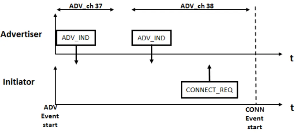
When an advertiser uses the Type 1 or the Type 4 events in Table 1.3, it permits a scanner to require additional information by sending SCAN_REQ PDU. When the advertiser uses these two types of event, it sends ADV_IND PDU or ADV_SCAN_IND PDU respectively to the advertising channels and then it listen on the same channel for the respond from a scanner while a scanner can respond to these packets with a SCAN_REQ PDU to obtain additional information. Figure 1.26 shows an example of the procedure of Type 1 event used advertising with a SCAN_REQ PDU reception from an active scanning. In this figure, an advertiser is sending ADV_IND to each of the three advertising channels, and when it is in the 38 channel, it receives a SCAN_REQ which can pass the advertising policy, then it responds this request by sending a SCAN_RSP in the same channel.
Fig. 1.26: Advertising event example with a scanner sending SCAN_REQ in channel 38 When an advertiser uses the Type 3 event in Table 1.3, it sends the non-connectable advertising indication (ADV_NONCONN_IND) to the advertising channels but without listening. Thus a scanner can obtain information by receiving this packet but it can’t respond to it.
Advertising & Initiating
When LL is in the initiating state, it opens a ScanWindow to listen on each advertising channel. When it receive ADV_IND PDU or ADV_DIRECT_IND PDU which is allowed by the initiator filter policy, it will respond with a CONNECT_REQ PDU to require a connection. The initiator enters to connection state after sending the CONNECT_REQ PDU.
When an advertiser uses the Type 1 or Type 2 events in Table 1.3 and it receives a CONNECT_REQ PDU, it will become a Slave by entering the connection state with come conditions. Figure 1.27 shows an example of the procedure of Type 1 event used advertising with a CONNECT_REQ PDU reception from an initiator.
Fig. 1.27: Advertising event example with an initiator sending CONNECT_REQ in channel 38
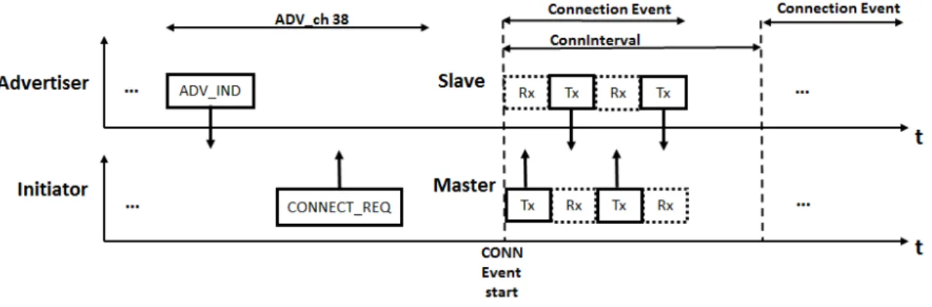
Connections
As we have talked before, an LL goes to the connection state when it sends a CONNECT_REQ PDU as an initiator or when it receives a CONNECT_REQ PDU as an advertiser. When an initiator enters the connection state it becomes a Master, and when an advertiser enters this state it becomes a Slave. They are allowed to communicate with Data channel PDUs. When an LL enters this state the connection is created. Then to establish this connection, there should be at least one successful Data packet reception.
The Master and the Slave choose a channel index and use it to exchange Data packets during the same connection event. The timing in connection state can be generally determined by two parameters:
• Connection event interval (connInterval): It defines the interval between two consecutive connection events;
• Connection slave latency (connSlaveLatency): It defines the number of connection events that the Slave has the right to skip but still with connection.
Both of the master and the slave use supervision timer detect a possible connection loss at any time during a connection. This timer counts the maximum time interval between two valid packet receptions and if this interval exceeds the predefined maximum interval, a supervision timeout will be created which will make an LL exit the connection state and go back to the standby state.
Fig. 1.28: Two LLs enter to connection event from advertising and initiating respectively During the packets exchange in a connection event, both Master and Slave indicate whether they have more data to send by using the MD bit in the packet header (cf. Fig. 1.28). If both of them don’t have any more data to send, the Master will close the event and the Slave won’t listen on the channel after its packets sending. If either of them or both still have data to send, the Master should maintain the event and the Slave has to listen on the channel after its packet sending.
3.5.
BLE Physical layer description
BLE physical (PHY) layer is the part where the transceiver is presented with which the analog signals are modulated or demodulated and exchanged through physical channels.
BLE radio operates in the 2.4 GHz Industrial, Scientific and Medical band (ISM) which is an unlicensed frequency band. The complete frequency range used by BLE is from 2.400 to 2.4835 GHz. In this range, BLE uses 40 channels which have the central frequencies as 2402 + k * 2 MHz, where k is from 0 to 39 (cf. Fig. 1.29). The three channels with indexes of 37, 38 and 39 are used as advertising channels to exchange broadcast data and to establish BLE connections. The rest 37 channels are data channels which are used to exchange data during BLE connections.
The communication in the ISM band could have lots of interference because there are other wireless technologies as WLAN and NFC, etc., which operate also in this band. So BLE uses frequency hopping (FH) technique to combat interference and fading. FH means that the RF signals are switched rapidly to different channel according to a pseudorandom sequence of the channel index.
The BLE modulation is the Gaussian Frequency Shift Keying (GFSK) with a modulation rate of 1 Mbit/s. The bandwidth-bit period product is fixed as 0.5 and the modulation index should be between 0.45 to 0.55. A binary one is represented by a positive frequency deviation and a zero is represented by a negative frequency deviation. GFSK principle will be introduced in the next subsection.
BLE is defined for a transmitter output power between 0.01mW to 10mW. The receiver sensitivity level is set to be less than or equal to -70 dBm, for a 0.1% BER.
3.6.
GFSK modulation
In the passband transmission, Frequency Shift Keying (FSK) is a digital modulation which converts the digital baseband signals (0 or 1) to passband frequency modulated signals. In the case of the binary FSK for example, two frequencies f1 and f2 are used to represent
binary information 0s and 1s respectively. Then the FSK modulated signal can be described by Eq.27, and wave form is like shown in Figure 1.30.
" "
" " (Eq.27)
Fig. 1.30: FSK example for transmitting “101”
FSK is widely used is because that the FSK modulated signals have better noise immunity in comparing with the amplitude modulated signals, and FSK modulated systems are less complicated for the demodulation.
Gaussian (GFSK) modulation is the Gaussian filter applied FSK modulation. GFSK uses a Gaussian filter to smooth the beginning of each digital symbol before the frequency modulation procedure. The Gaussian filtering avoids the high frequencies due to the switching, and thus reduces the signal spectral bandwidth which will reduce the adjacent channel interference.
3.7.
Direct and indirect angle modulation
It is worth to mention that there are two extension types of angle modulation, which are the indirect FM and the indirect PM.
A PM RF signal can be described as
, (Eq.28) where is proportionally constant and is the baseband signal.
While an FM RF signal is given by Eq. 29.
, (Eq.29) where is also a proportionally constant.
As the frequency and the phase can be converted into each other with integration and derivation, the angle modulation can be extended to four methods as shown in Figure 1.31. They are the direct and the indirect FM, and as the direct and the indirect PM.
Fig. 1.31: Angle modulations: (a) Direct FM; (b) Indirect FM; (c) Direct PM; (d) Indirect PM If we firstly differentiate the baseband signal and then realize an FM, we will obtain a PM signal (cf. Fig. 1.31 (d)). This method is called indirect PM. And if we firstly integrate the baseband then realize a PM, we will obtain an FM signal (cf. Fig. 1.31 (b)). This method is called indirect FM.
4.
SystemC
toolset : Mixed signal simulation tools
4.1.
Introduction
In communication system design, there are various modeling tools and languages. Designs will be efficient in time and reliability only if we choose the ones that correspond to our design requirements. In this subsection, we will give brief introductions of some common
modeling languages and tools, then we will focus on SystemC tools introductions which is chosen for this work, and the interface establishments between the models of different domains described in SystemC tools [16].
4.2.
SystemC
SystemC is a set of C++ classes and macros for system level modeling, design and verification [17]. On one hand, SystemC has semantic similarities to hardware description languages such as VHDL and Verilog. On the other hand, it allows modeling software components by using directly C/C++ code by inheriting all of the advantages of C++ like the rich language constructs and data types which always make hardware designers reduce the time and efforts of work. SystemC supports the design in different abstraction levels so that designers can model either a large system in a very high abstraction level or an analog timed block with the predefined electrical primitives. Basic SystemC is based on a Discrete Event (DE) model of computation in which a scheduler maintains a time-sorted list of events, executes them accordingly and updates signals before increasing the simulation time. SystemC-DE can be used for event-driven models. In particular, two specific models of computation are available, i.e., RTL to model clocked behavior as well as bit-accurate signals and TLM to model interactions through function calls.
4.3.
SystemC‐AMS
SystemC provides an extension to model analog and mixed signal (AMS) components; in particular, three specific models of computation are available [17]:
• Timed Data Flow (TDF). It allows to model a system as a sequence of blocks producing and consuming data samples with a user-defined rate. TDF can be used for time-driven models. It permits to describe also discretized continuous-time systems, e.g., by using Laplace transfer functions.
• Linear Signal Flow (LSF). It supports natively continuous-time models by combining primitives such as addition, gain, integration, derivative, and delay operators. Discretization should not be addressed explicitly by the user.
• Electrical Linear Network (ELN). It supports natively continuous-time models by combining predefined linear electrical components, such as resistors and capacitors. Their characteristics are used to describe the continuous-time relationships between voltage and current levels.
4.4.
Verilog
‐AMS, VHDL‐AMS
Verilog-AMS (respectively VHDL-AMS) is the analog and mixed signal extension of the Verilog HDL (respectively VHDL). It is used to model blocks with behavioral or
structural modules encapsulate with ports and additional parameters. It simulates the analog behaviors with conservative solution which is the Kirchhoff's Potential and Flow Laws.
Previous works were led to the EpOC laboratory on the hierarchical modelling of building blocks of a RF transceiver by using the language VHDL-AMS [18], as well as on the simulation of a BT communication [19].
4.5.
Matlab
Matlab is a powerful worldwide used tool developed by MathWorks. It is based on C language and is usually used for matrix calculations, functions plotting, ect., and it can interface with programs written in C, C++, Java and Python. Applying for embedded system design, Matlab is also a data flow simulator. It is able to model RF analog systems containing non-idealities and the additional Simulink packet is easy and intuitive for models description. But it is limited in simulation speed for RF system simulation, not to mention a complete wireless communication system.
The coupling between Matlab and VHDL-AMS [20] already allowed to realize simulations system multi-engine and multi-level of BT communications within the EpOC laboratory: thesis of Benjamin Nicolle [19], Alexandre Lewicki [21] and Lucas Alves Da Silva [13]. An article of synthesis, summarizing all these works, was published in Microelectronics Journal [22].
4.6.
Mixing SystemC MoCs
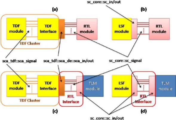
Previous sections introduced the modeling strategies for communications. Even when only SystemC is considered, different models of computation can be used. In particular, this section aims at presenting how to mix TDF, LSF, RTL, and TLM MoCs.
Figure 1.32 (a) gives an overview of the architecture used to interface a TDF component with an RTL component. In this case, since SystemC Discrete Event processes are not allowed within TDF modules, an adjunctive TDF module has been inserted to replicate the TDF interface of the component as an RTL interface by using sca_tdf::sca_de ports. This architecture allows to maintain unchanged the TDF implementation of the component.
Figure 1.32 (b) gives an overview of the architecture used to interface an LSF component with an RTL component.
Even if LSF descriptions are used to specify continuous time components (i.e., ODE), they allow the presence of any classic SystemC process (i.e., SC_THREADs or SC_METHODs) obeying to the standard Discrete Event model of computation used by basic SystemC. Moreover, input and output ports of LSF clusters can be written or read by discrete processes.
![Figure 1.1 shows an example of a 2 nodes wireless communication system [7]. A complete wireless system like this can be divided into three different domains as: Digital Signal Processing (DSP), Analog BaseBand (BB) and Radio Frequency (RF) transceiver,](https://thumb-eu.123doks.com/thumbv2/123doknet/12926647.373757/16.892.120.776.603.763/wireless-communication-complete-different-processing-baseband-frequency-transceiver.webp)