HAL Id: cea-02341034
https://hal-cea.archives-ouvertes.fr/cea-02341034
Submitted on 31 Oct 2019HAL is a multi-disciplinary open access archive for the deposit and dissemination of sci-entific research documents, whether they are pub-lished or not. The documents may come from teaching and research institutions in France or abroad, or from public or private research centers.
L’archive ouverte pluridisciplinaire HAL, est destinée au dépôt et à la diffusion de documents scientifiques de niveau recherche, publiés ou non, émanant des établissements d’enseignement et de recherche français ou étrangers, des laboratoires publics ou privés.
Study of the electrografting of two different diazonium
salts on patterned gold electrodes
Frédéric Lebon, Y.-P Lin, H Casademont, R Cornut, B Jousselme, V Derycke
To cite this version:
Frédéric Lebon, Y.-P Lin, H Casademont, R Cornut, B Jousselme, et al.. Study of the electrografting of two different diazonium salts on patterned gold electrodes. 9th International Conference on Molecular Electronics and Bioelectronics, Jun 2017, Kanazawa, Japan. �cea-02341034�
Study of the electrografting of two different diazonium salts on patterned
gold electrodes.
F. Lebon, Y.-P. Lin, H. Casademont, R. Cornut, V. Derycke, B. Jousselme
LICSEN, NIMBE, CEA, CNRS, Université Paris-Saclay, CEA Saclay 91191 Gif-sur-Yvette Cedex
E-mail: [email protected]
Despite the recognized potential of organic molecules for electronics, only very few types of devices (like OLEDs) incorporating thin molecular layers as active elements, have reached the level of industrial applications. Two major issues slowdown such integration: (i) the way of incorporating molecules in electronic systems is usually incompatible with device miniaturization, and (ii) thin molecular layers suffer from a limited robustness notably toward back-end process steps.
The properties of molecular layers are commonly studied using either self-assembled monolayers (SAMs) or thick non-patterned layers prepared by spin or dip coating. Electrografting by reduction of diazonium salts provides an efficient alternative to these methods. It leads to robust covalent organic thin films of adjustable thickness (typically in the 5 to 50 nm range) and rich functionality. These films can be assembled on all conducting or semi-conducting electrodes, are compatible with lithography and allows the selective grafting of different electrodes of the same chip with different molecules.
However, the integration of such versatile organic thin films in functional devices requires a deep understanding and thorough control of their growth mode. This presentation aims at elucidating the influence of different parameters on the formation of molecular thin films based on two kind of diazonium salts: one leading to an ultrathin insulating layer that can be used as a nanodielectric in transistors[1], and one that can be used to form resistive memory devices[2].
[1] H. Casademont, L. Fillaud, X. Lefèvre, B. Jousselme, V. Derycke, J. Phys. Chem. C, 2016, 120, 9506−9510 [2] Y.-P. Lin, C.H. Bennett, T. Cabaret, D. Vodenicarevic, D. Chabi, D. Querlior, B. Jousselme, V. Derycke, J.-O. Klein, Scientific Reports, 2016, 6, 31932.
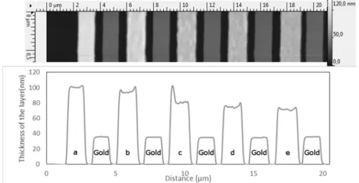
Figure 1. AFM image of gold electrodes grafted in different conditions with a TBPFe diazonium salt (up) and its corresponding profile (down). The electrodes a, b, c, d and e are
grafted while the gold electrodes are used as a height reference.