HAL Id: hal-01021074
https://hal.archives-ouvertes.fr/hal-01021074
Submitted on 15 Jul 2014HAL is a multi-disciplinary open access
archive for the deposit and dissemination of sci-entific research documents, whether they are pub-lished or not. The documents may come from teaching and research institutions in France or abroad, or from public or private research centers.
L’archive ouverte pluridisciplinaire HAL, est destinée au dépôt et à la diffusion de documents scientifiques de niveau recherche, publiés ou non, émanant des établissements d’enseignement et de recherche français ou étrangers, des laboratoires publics ou privés.
Smallest aspect-ratio form-birefringence half-wave plate
Thomas Kampfe, Pierre Sixt, Denis Renaud, Armelle Lagrange, Fabrice
Perrin, Remi Torres, Guillaume Gomard, Olivier Parriaux
To cite this version:
Thomas Kampfe, Pierre Sixt, Denis Renaud, Armelle Lagrange, Fabrice Perrin, et al.. Smallest aspect-ratio form-birefringence half-wave plate. 10th International Workshop on High Aspect Ratio Micro and Nano System Technology (HARMNST), Apr 2013, Berlin, Germany. pp.Poster T31. �hal-01021074�
Smallest aspect-ratio form-birefringence half-wave plate
T. Kaempfe
1*, P. Sixt
2, D. Renaud
2, A. Lagrange
2, F. Perrin
2, R. Torres
3, G. Gomard
4, O. Parriaux
11
Laboratoire Hubert Curien UMR CNRS 5516, Université de Lyon à St-Etienne, France
2
LETI, 17 Rue des Martyrs, F-38054 Grenoble
3
ALPhANOV, 351 Cours de la Libération, F-33403 Talence
4
Université de Lyon, INL UMR CNRS 5270A, F-69134 Ecully
*
[email protected]
, tel. +33477915825
Form-birefringence elements
Subwavelength 0th order gratings permit to create a phase-shift between the polarized 0th order grating modes propagating down the slits and grooves of a binary corrugation, and to transform the polarization of an incident beam. The phase-shift per unit height of the grating is an increasing function of the refractive index difference between ridges and grooves. If the ridges are made by photolithography in a resist or by polymer embossing, the low refractive index leads to a very large corrugation aspect ratio (approx. 4 for a half-wave phase-shift) that is difficult to fabricate and/or provides insufficient mechanical stability. If the ridges are made in a high index non-organic material (e.g. a semiconductor) the needed depth is reduced (although still notably larger than 1 for a half-wave phase-shift). However, another problem is now encountered: due to a more significant Fabry-Perot effect between the upper and lower boundaries of the 0th order grating [1] high transmission is guaranteed only if its resonance condition is ensured for both polarizations simultaneously. The three conditions ( phase-shift between TE and TM and both Fabry-Perot resonances) are impossible to achieve simultaneously if the corrugation is made by directly etching the substrate (same material for ridges and substrate) unless the grooves are very deep which imposes difficult etching conditions [2]. Using an inventive design by phase management of the involved grating modes [2] we have found that all three conditions can indeed be satisfied in a binary grating of reasonable aspect ratio (still larger than 1) when the substrate has a refractive index notably smaller than the ridges.
Smallest aspect-ratio half-wave plate
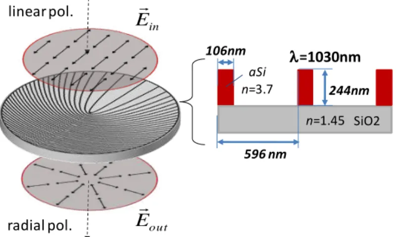
The obtained electromagnetic condition is wavelength dependent; thus a choice was made for a Yb:YAG laser in the objective of defining a spatially resolved polarization rotating element for this type of laser, creating radially polarized light. Figure 1 sketches the structure to be fabricated. The substrate is fused quartz, having a grating on top made of well known solar cell PECVD amorphous silicon [3] (a-Si) of 244 nm thickness.
out
E
linear pol. radial pol. inE
596 nm 106nm 244nm SiO2 n=1.45 aSi n=3.7 =1030nmFig. 1 Aspect-ratio minimized a-Si half-wave 0th order grating for creating radial polarization .
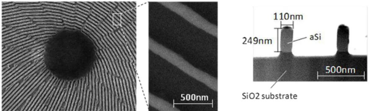
The photolithography of the 596 nm period grating was made by hard-contact chromium mask transfer followed by wet-chemical thinning of the photoresist ridges so as to end up with ridges of about 100 nm width. A reactive ion etching process was then applied to transfer the resist profile into the amorphous silicon layer down to the quartz surface. Figure 2 shows SEM images of a cleaved a-Si grating. The optical function of the element was assessed experimentally exhibiting locally a transmission larger than 97% for both polarizations and an optical phase-shift between polarizations of close to the desired 180 degrees. Preliminary laser flux resistance tests were made with a femtosecond Yb:YAG laser beam showing that the damage threshold of the fabricated element is close to the machining operation conditions of this laser [4], leading to the conclusion that a more reliable microstructuring technology will give a sufficient security margin for an operation without requiring beam diameter expansion.
Toward a reliable manufacturing technology
The needed aspect ratio limited structure can ideally be manufactured by means of high-end microelectronic technology starting with the writing of a chromium reticle followed by the 4x reduction factor step and repeat projection by means of a 248 nm stepper onto a 200 mm diameter borofloat glass wafer with a 250 nm TEOS oxide hard mask on top. The photolithography of the 613 nm period grating was made by KrF stepper lithography. Before proceeding to the ICP etch, a controlled trimming of the resist ridges is still needed to obtain the specified duty cycle and aspect-ratio with an ideally 113nm wide ridge basis.
Fig. 2. SEM image of the central region (left) and of a cross-section (FIB-slice) of the half-wave laboratory prototype for creating radial polarization
Beyond the achievement of this particular polarization-rotating element, the present undertaking aims at concretely evaluating what microelectronic technology can do for the batch manufacturing of wavelength-scale diffractive elements for the processing of free space waves. The presentation will report on the technological problems, the structure uniformity at the wafer level and the yield. A manufacturing cost estimate will also be made.
References
[1] G. Lerman and U. Levy, "Generation of a radially polarized light beam using space-variant subwavelength gratings at 1064 nm," Opt. Lett. 33, pp. 2782-2784 (2008)
[2] T. Kämpfe and O. Parriaux, "Depth-minimized, large period half-wave corrugation for linear to radial and azimuthal polarization transformation by grating-mode phase management," J. Opt. Soc. Am. A 28, pp. 2235-2242 (2011)
[3] T. Kaempfe, S. Tonchev, G. Gomard, C. Seassal and O. Parriaux, "Hydrogenated amorphous silicon microstructuring for 0th order polarization elements at 1.0µm-1.1µm wavelength," IEEE Photonics Journal 3, pp. 1142-1148 (2011)
[4] R. Torres, Th. Kaempfe, M. Delaigue, O. Parriaux, C. Hönninger, J. Lopez, R. Kling, and E. Mottay, 13th LPM, Catholic University of America, Washington DC, 12-15 June 2012.