HAL Id: tel-01559004
https://tel.archives-ouvertes.fr/tel-01559004
Submitted on 10 Jul 2017HAL is a multi-disciplinary open access
archive for the deposit and dissemination of
sci-L’archive ouverte pluridisciplinaire HAL, est destinée au dépôt et à la diffusion de documents
Development and Study of Organic Polymer Resistive
Memories For Crossbar Architectures
Micaël Charbonneau
To cite this version:
Micaël Charbonneau. Development and Study of Organic Polymer Resistive Memories For Crossbar Architectures. Micro and nanotechnologies/Microelectronics. Université de Grenoble, 2012. English. �NNT : 2012GRENT116�. �tel-01559004�
THÈSE
Pour obtenir le grade de
DOCTEUR DE L’UNIVERSITÉ DE GRENOBLE
Spécialité : Microélectronique et Nanotechnologies
Arrêté ministériel : 7 août 2006
Présentée par
Micaël CHARBONNEAU
Thèse dirigée par « GérardGHIBAUDO»
Préparée au sein du Laboratoire des Technologie Mémoires Avancée du CEA-LETI
dans l'École Doctorale EEATS
Etude & Développement de Points
mémoires Résistifs Polymères
pour les Architectures Crossbar
Thèse soutenue publiquement le 19 Janvier 2012, Devant le jury composé de :
M. Jae Gun PARK
Professeur à l’université d’Hanyang (Seoul, Corée du Sud), Président
M. Dominique VUILLAUME
Directeur de Recherche au CNRS-IEMN de Lille, Rapporteur
M. Georges MAILLIARAS
Professeur à l’ENS Mines - Gardanne, Rapporteur
M. Gianfranco CEROFOLINI
Docteur Ingénieur de recherche à l’université de Milan (Italie), Membre du jury
M. Julien BUCKLEY
Docteur Ingénieur de recherche au CEA Grenoble, Membre du jury
Mme Raluca TIRON
Docteur Ingénieur de recherche au CEA Grenoble, Membre du jury
Mme Barbara DE SALVO
Docteur Ingénieur de recherche au CEA Grenoble, Membre du jury
M. Gérard GHIBAUDO
« Chercher à connaitre n’est souvent qu’apprendre à douter »
Madame Deshoulières
« If A is success in life, then A equals x plus y plus z. Work is x; y is play; and z is keeping your mouth shut. »
Remerciements
Tout d’abord je souhaiterais remercier Monsieur Dominique Vuillaume, Directeur de Recherche CNRS, et le Professeur Georges Malliaras pour m’avoir fait l’honneur d’être rapporteurs de ce travail de thèse. J’ai été particulièrement honoré et personnellement touché par la présence du Professeur Jae-Gun Park en tant que président de mon jury. Je remercie également M. Giofranco Cerofolini et Monsieur Romain Coppard pour leur participation à ce jury et leurs remarques avisés.
Toute ma reconnaissance va bien sûr à l’équipe encadrante qui, par son implication active de tous les jours a rendu possible et fructueuse cette formidable aventure. J’ai eu la chance d’avoir pu réaliser ce travail dans les meilleures conditions qui puisse être sur les plans matériels et humains. Je pense en premier lieu à mes encadrants de thèse qui ont formé une combinaison complémentaire de compétences et de qualités humaines riches pour mon épanouissement. Merci à toi Raluca pour ton énergie, ta curiosité et ta motivation à toujours aller de l’avant. Julien, je souhaite te remercier pour ta disponibilité, tes conseils avisés et ton soutien sans faille ainsi que pour toutes les discussions que j’ai eu plaisir à partager avec toi. Je voudrais également remercier Samir co-encadrant du stage qui a précédé cette thèse. Je veux aussi remercier particulièrement ma chef de laboratoire Barbara De Salvo qui m’a permis de travailler sur ce sujet exploratoire et m’a soutenu pour partager ces travaux en conférences ou même à l’autre bout du monde. Un grand merci à Gérard Ghibaudo, mon directeur de thèse pour sa disponibilité, ses conseils de qualités et les discussions que nous avons pu avoir. Enfin, je voudrais remercier Nathalie qui nous a rejoint dans l’aventure sur cette fin de thèse, a pris le relais et m’a permis de continuer l’analyse psychologique de ces enfants terribles des mémoires avec des séances de si-et-seulement-si mémorables.
Je veux aussi chaleureusement remercier tous ceux qui ont contribué à ce travail. En premier lieu ceux qui m’ont permis de fabriquer les échantillons qui ont fait le succès de cette aventure. Je pense à Milène, Sébastien, Jean-Paul le premier explorateur de la PTA et sauveur des thèses de notre promo, Guillaume ,Thibault, Helge et tout le groupe technique de la PTA qui ont tous partagé leur savoir-faire et souvent de leur temps pour m’aider dans la fabrication des dispositifs. Tout cela aurait été difficile sans vous. Un gros merci à Marc G. pour son implication dans les Lots, sa disponibilité et ses tuyaux sur OLGA, les carnets de lots et le monde merveilleux des filières au 41. Je veux aussi remercier les membres de l’expédition IRMA avec qui j’ai eu le plaisir de partager la roadmap et ses rebondissements: Carine, Jean-François, Françoise, Hélène et Cyril aussi.
Je veux aussi remercier tous mes collègues spécialistes de l’analyse physico-chimique qui ont participé à la compréhension de ce nouveau matériau par le biais d’études souvent délicates. Je remercie Claire pour les analyses thermiques mais aussi pour ses conseils de survie au 41, Mathieu et Jean-Paul pour la superbe collaboration qu’on a pu avoir en ToF-SIMS, un énorme merci à Denis éminent spécialiste de l’AFM avec qui j’ai aimé travaillé et pour les superbes manips réalisées avec Nathalie, également Christophe, Névine et Denis Rouchon pour les analyses spectro et Raman souvent délicates sur ces composites. Merci également à Christophe, David et Stéphane pour les manips de litho sur ces résines frelatées.
Je veux aussi remercier tout le groupe de test électrique en particulier la team des grands sages, Jacques le big boss, Patrick le Mac Gyver du BCA et Denis mon ami du 20h30 passé pour m’avoir laissé squatter de manière souvent très intensive les SIAMs. Je m’excuse par avance de l’usure anticipée du SIAM6. Je veux aussi salué la ténacité de tous mes compagnons de galères qui ont subit les mêmes lots que moi de joie mais aussi de déception devant l’écran implacable d’un 4156. Bravo à tous ces chercheurs passionnés et merci pour la jovialité partagée lors de nos discussions malgré l’adversité, l’heure avancée et les lots scrapés. Merci aussi pour les petits arrangements de créneaux que j’ai pu avoir avec beaucoup d’entre vous !
Enfin je voudrais remercier tous ceux qui ont fait ma vie quotidienne au jour le jour pendant plus de trois ans et demi. En premier, mes collègues qui font du LTMA ce cocon ou il fait bon vivre et partager : merci a Marc et Jean-François pour le café et leur idées farfelues dès 9h, Carine pour ta curiosité malicieuse et ta source de potins intarissable, Alain et Véro pour votre gentillesse et bonne humeur contagieuse, Julien pour tes bon conseils et ton goût du débat et de la discussion, Eric pour ta bonne humeur et tes talents de VRP, Gab pour ta disposition à te sacrifier en premier pour dire ou faire les conneries qui nous font tous marrer. Tous à chacun vous êtes le cœur de ce beau labo. Et puis il y a bien sûr tous les intermittents de la science qui apportent chaque fois une nouvelle facette de personnalités, d’expériences et d’anecdotes. Big up à tous mes grands frères et sœurs thésards pour leurs expériences partagées et leur bonne humeur : Joshna, Fred, Vincent, Emilie, Tizianna, Alex, Michael, Jean-Paul, Marc, Perrine, Louis, Guillaume. Une pensée particulière pour mes collègues de promo Milène et Paul-Henry aux sujets aussi «prometteurs pour le futur» et «amonts» que moi. Un merci très spéciale à Milène ma «jumelle de thèse» qui a sauvé ma thèse plus d’une fois avec ses coups de pouce PTA, les pointes AFM détruites, les lithos, les dépannes administratives et j’en passe… Merci surtout pour avoir partagé toutes ces pauses café et escapades à H1, de chouettes moments anti-déprimes obligatoires pour survivre aux thèses amonts. Et puis, je voudrais saluer tous nos suivants que j’ai pus croiser Paolo, Quentin, Gabriele, Cuiqin, Veeresh, Thomas et «Just because of the scholar system», une dédicace spéciale pour mon co-bureau Giorgio, sa TDM, nos divagations sur les oxygen vaccancies et la magnifique sculpture de rédaction.
Pendant cette thèse j’ai aussi eu la chance d’avoir été accueilli pendant 5 mois à l’autre bout du monde en Corée par des personnes d’une gentillesse et d’une attention exceptionnelles. Ils m’ont fait partager leur quotidien, leur mode de vie, mais aussi leur culture ainsi que des moments importants de leur vie. I would like to thank Professor J-G Park and Professor Shim for welcoming me in their Lab. I have been particularly glad and proud to join their researchers in Hanyang University. I would like also to warmly thank all the students who welcome me not only as colleague but also as special guest. You have been great ambassadors of your country making me discover some of your life and culture. Therefore I spent really nice time in Korea and will keep in memories my extra life shared with you. Of course I would like to thank in first my team : the PBD family with Hyun-Min, Jong-Dae, Kyoung-Cheol, Jae-Sung, Jung-Nam but also all the people I get the chance to interact Dal-Ho, In-jee, Mi-Hee, Seung-Wook,Jong-Sun, Tae-Hyun, Jong-Young, Hee-Sub, Jae-Hyung, Ji-Heon, Jae-Hyoung, Seung-Hyun, Seong-Gwang, Yeon-Hui, Du-yeong, Hyun-Ki, Dong-Hyun, Min-Ha, Myung-Jin, Jae-Woo, Hyoung-Rae. During that adventure, most of you turn in real friends and I sincerely look forward meeting you
Je voudrais aussi remercier tous les étudiants étrangers de la résidence universitaire que j’ai eus le plaisir de côtoyer dans mon extra-life coréenne. Merci pour m’avoir fait revivre ce formidable esprit Erasmus. Une dédicace spéciale à Max, Alexandro, Renato et mon colloc Bhuvan pour ces séances de décompression mémorables.
Enfin je dois remercier ceux qui ont toujours été là pour m’encourager et me soutenir à aller de l’avant mais aussi surtout pour m’avoir sorti la tête de la thèse et me rappeler l’essentiel : je pense à ma famille et mes amis proches. Merci à tous mes amis grenoblois pour m’avoir permis « d’estampiller fête » à gogo ces trois années. Merci au crew de l’ENSERG et associés : Mich, Laure, Jo, Edith, Alex, Isa, Amélie, Sylvain, Fab, Annick, Sven et Céline, Loubarth, Bertrand et Franscesca. Une mention spéciale pour le CBC qui m’a suppléé pendant mon escapade coréenne et pour toutes ces soirées gastronomiques et intellectuellement riches. Merci à Repi et Nanou pour cette combinaison unique Cèpes-Chazy, Scotch on the Rock, Litter-Kwitter. Merci un million de fois à Audrey et Nieu pour vos petits plats et traquenards dont je raffole. Vous avez de loin été notre deuxième maison.
Bien sûr, je voudrais remercier l’ensemble de ma famille et en particulier mes parents qui m’ont appris à aimer apprendre et découvrir toujours plus, oubliant les préjugés. Merci également à mes sœurs et mon petit frère qui ont fait de moi l’avant-garde de la fratrie et m’oblige à me tenir un peu à carreaux. Je veux aussi remercier la succursale vendéenne de Voreppe : 800km en15 min. un extra booster sur lequel j’ai pu me reposer plus d’une fois avant de repartir gonflé à bloc. Merci à tous pour votre support, les moments partagés, et votre implication jusqu’au pot de thèse qui a super assuré : en bon chauvinisme, vous êtes justes les meilleurs.
Finalement, je voudrais remercier celle à qui je dois le plus, qui a été à mes côtés depuis le début et avec qui j’ai partagé cette aventure et déjà plusieurs autres. A l’instar du pot de thèse (sans contestation le chapitre le plus réussi de ce doctorat), elle a été une clé maitresse du bon déroulement de cette thèse. Elle a su m’attendre et me supporter dans mes rêveries et aventures, a eu la tâche délicate de me déconnecter quand j’en faisais trop ou de me remotiver dans les moments plus difficiles en m’apportant son énergie, ses conseils et son aide. Merci Ha Lan.
Merci à vous tous que j’ai eu la chance de croiser sur le chemin. Vous constituez chacun à votre manière une partie de ce travail et de ce que je suis. A bientôt !!!
-CONTENTS
-Contents
Acronyms ... vii
Notations... viii
General Introduction... 1
I
NON-VOLATILE STORAGE TECHNOLOGIES AND
ORGANIC ELECTRONIC MEMORIES ... 3
I.1 Overview on Non-Volatile Memory Technologies ... 5
I.1.1 History of Storage Technologies and Technical Requirements...5
I.1.1.a From Early Stages to the Emergence of Machines ...5
I.1.1.b Emerging of Technologies for Electronics ...6
I.1.1.c Requirements for memory Technologies ...7
I.1.2 Current Memory Market, Technologies and Challenges...7
I.1.2.a Semiconductor Memory Technologies...8
I.1.2.b Evolutions & Requirements for future generations...9
I.1.2.c Limitations of Flash NVM technologies ...10
I.1.3 Development of New Technologies & Opportunities for Resistive Memory...10
I.1.3.a Candidates for Emerging Memory technologies...10
I.1.3.b Opportunities for resistive memories regarding integration ...11
I.1.3.c Performance of resistive memories ...12
I.1.4 Conclusions ...13
I.2 State of the Art of Organic based Memory Devices ... 14
I.2.1 Interest of organic materials for future electronics...14
I.2.2 Molecular memory devices...14
I.2.2.a The Capacitive Memory Approach ...14
I.2.2.b Resistive Memory Approach and Molecular Crossbar ...16
I.2.2.c Challenges for molecular scaled approach ...18
I.2.3 Organic Thin Films for Memory Devices ...19
I.2.3.a The Capacitive Memory Approach ...19
I.2.3.b The Resistive Memory Approach...20
I.2.4 Perspectives for organic memory devices...21
I.3 Development of Organic Thin Film Resistive Memories ... 22
I.3.1 Materials and Device Integration ...22
I.3.1.a Organic composition ...22
I.3.1.b Electrodes...23
I.3.1.C Memory cell Scaling ...23
I.3.1.d Memory Layer Stacking (3D) ...24
I.3.2 Electrical Performances ...25
I.3.2.a Resistive switching...25
I.3.2.b Retention...26
I.3.2.c Reversibility ...27
I.3.2.d Programming window and reproducibility ...27
I.3.2.e Multilevel capability (MLC) ...28
I.3.2.f Endurance ...28
I.3.2.g Access Time...28
-CONTENTS
-I.3.3.a Molecular mechanisms ...30
I.3.3.b Electronic mechanisms ...31
I.3.3.c Formation of Metallic or Carbon rich Filaments...31
I.3.3.d Switching in Interfacial Oxide...32
I.3.3.e Summary...33
I.3.4 Requirements & Challenges for Organic Resistive Memory Technologies...33
I.4 Our Approach ... 35
I.4.1.a Process selection ...35
I.4.1.b Material composition...35
I.4.1.c Characterization strategy ...35
I.5 Conclusions of Chapter I... 37
Appendix I.A: ITRS Roadmap for Memory Devices... 38
II
FABRICATION & MATERIAL CHARACTERIZATION OF
(PMMA:C
60) NANOCOMPOSITES FOR MEMORIES... 41
II.1 Development of (PMMA:C60) nano-composites... 43
II.1.1 Materials & Components description ...43
II.1.1.a Introduction to Composite materials ...43
II.1.1.b Interest of organic nanocomposite approach for experimental studies ...43
II.1.1.c Poly-methyl-methacrylate (PMMA) Insulating Polymer matrix ...44
II.1.1.d Fullerene (C60) semi-conductive spherical molecules...45
II.1.2 Solution synthesis of organic Nanocomposites ...45
II.1.3 Thin-Film Processing...46
II.2 Material characterization of nanocomposite films ... 48
II.2.1 Physical properties of (PMMA:C60) thin film...48
II.2.1.a Surface Roughness...48
II.2.1.b In - film distribution...49
II.2.1.c Thermal properties ...50
II.2.2 Quantification and in-layer Distribution ...51
II.2.2.a UV-Vis Spectroscopy - Quantification ...51
II.2.2.b ToF-SIMS - Quantification & Distribution...53
II.2.3 Nano-patterning capabilities...55
II.2.3.a Through E-Beam Lithography ...55
II.2.3.b With Nano-Imprint Lithography process ...55
II.2.4 Conclusions on Nanocomposite Characterization...56
II.3 Impact of Thermal annealing above the glass transition... 57
II.3.1 Aggregation of C60 above the Tg...57
II.3.2 Conclusions and Perspectives on Nanocomposite organization study ...58
II.4 Test Devices for electrical characterization... 59
II.4.1 Top electrodes processing on organic materials ...59
II.4.2 Macrostructures for straight-forward electrical characterization ...59
II.4.3 Structures for electrical downscaling...60
II.4.4 Design of Advanced structures towards integration...60
II.5 Conclusions of Chapter II... 61
-CONTENTS -
III
CAPACITIVE CHARACTERIZATION ON (PMMA:C
60) IN
MOIS STRUCTURES ... 65
III.1 Introduction to C-V Characterization on MIS... 67
III.1.1 Interest of MIS structure for (PMMA:C60) characterization ...67
III.1.2 Electrical C-V behavior for ideal MIS structure...67
III.1.3 C-V characteristics for Non-ideal MIS Structures ...70
III.1.3.a Metallic Gate, with charge free insulator and interface ...70
III.1.3.b Non-ideal Insulator...71
III.1.3.c Defects at the semiconductor/insulator Interface ...71
III.1.3.d Impact of charge on C-V characteristics ...72
III.2 Characterization of PMMA in MOIS devices ... 73
III.2.1 Structure for charge trapping analysis ...73
III.2.2 C-V Characterization of PMMA reference devices ...73
III.2.2.a C-V characteristics and unusual inversion behavior ...73
III.2.2.b Unexpected Frequency Behavior ...75
III.2.2.c Model of Permanent Inversion Layer...76
III.2.2.d Influence of Device Area...76
III.2.2.e Hysteresis & Voltage Dynamic in Inversion ...78
III.2.3 Conclusion for PMMA reference device...79
III.3 Charge trapping memory effect controlled by C60 doping ... 80
III.3.1 Hysteresis on C-V characteristics with C60 doping ...80
III.3.2 A charge trapping related mechanism...81
III.3.3 Time-Voltage Dependence ...83
III.3.4 Conclusions & Perspectives...84
III.4 Conclusions of Chapter III ... 85
Appendix III.A: Inversion ratio with lateral Fictive source drain ... 86
IV
UNIPOLAR MULTILEVEL RESISTIVE MEMORY EFFECT
IN (PMMA:C60) WITH INERT ELECTRODES. ... 87
IV.1 Resistive behavior of (PMMA:C60) layers in MOM Structures... 89
IV.1.1 Screening for Current hysteresis ...89
IV.1.1.a Influence of C60 doping upon leakage current ...89
IV.1.1.b Electrical behavior of thermally annealed nanocomposite layers...90
IV.1.2 Conditions for Hysteresis and NDR behavior ...92
IV.1.2.a Specific material processing conditions...92
IV.1.2.b Specific electrical conditions-The forming operation...92
IV.1.3 Negative Differential Resistance behavior ...93
IV.1.4 Conclusions on the electrical behavior of (PMMA:C60) layers with Platinum electrodes...94
IV.2 Memory Operation for NDR based devices ... 95
IV.2.1 Unipolar Multilevel Memory Effect ...95
IV.2.1.a Unipolar programming through polarization in NDR ...95
IV.2.1.b Multilevel operation...96
IV.2.2 Low field stability and Data Retention...97
IV.2.3 DC Memory cycling...97
IV.2.4 Reproducibility and variability ...98
IV.2.4.a Cycle-to-Cycle distributions...98
IV.2.4.b Device-to-Device distributions... 100
-CONTENTS
-IV.2.5.a Pulse Amplitude... 101
IV.2.5.b Pulse Length... 102
IV.2.6 Electrode Area Downscaling ...103
IV.2.7 Conclusion and Overview on performances ...105
IV.3 Detailed Characterization for behavioral understanding ... 106
IV.3.1 Identification of device behavior ...106
IV.3.2 Quasi-static Forming and Negative Differential Resistance ...106
IV.3.2.a Impact of forming operation on NDR... 107
IV.3.2.b Reproducible Quasi-Static NDR characteristics... 107
IV.3.3 On Multilevel Steady States...108
IV.3.3.a Resistance programming trough NDR... 108
IV.3.3.b Conduction Characteristics for Steady States ... 108
IV.3.3.c Common conduction characteristic for NDR and Steady State ... 110
IV.3.4 Details of switching transitions ...111
IV.3.4.a Dynamic dependence... 111
IV.3.4.b Dependence upon the initial resistance... 111
IV.3.5 Quasi-static description of device operation...112
IV.3.5.a Hypothesis for conduction modeling ... 112
IV.3.5.b Simple quasi-static behavioral systems ... 113
IV.3.5.c Implementation in SPICE and Simulation Results ... 114
IV.3.6 Conclusions and Perspectives...116
IV.4 Conclusions of Chapter IV... 117
Appendix IV.A: Equivalent Circuits For quasi-static behavioral modeling... 119
V
STUDY OF BIPOLAR RESISTIVE MEMORY EFFECTS IN
(PMMA:C60) USING OXIDIZABLE ELECTRODES... 121
V.1 Bipolar resistive switching in (PMMA:C60) with oxidizable bottom electrode ... 123
V.1.1 Device structures for the study of the impact of the interfacial oxide...123
V.1.2 Resistive behavior with inert bottom electrode...124
V.1.3 Bipolar Hysteresis with oxidizable bottom electrode (MiOIM)...125
V.1.3.a Current hysteresis induced by bipolar sequences ... 125
V.1.3.b Different available conduction modes... 126
V.1.4 Impacts of C60 doping concentration on Hysteresis windows ...127
V.1.5 Conclusions on the Impact of oxidizable bottom electrode...128
V.2 Detailed characterization in bipolar memory operation ... 129
V.2.1 Non Volatile Resistive Memory Operation ...129
V.2.2 READ-ERASE - Influence of Positive sequences on hysteresis...129
V.2.3 WRITE - Influence of Programming Conditions on hysteresis ...131
V.2.3.a Influence of the Programming Voltage... 131
V.2.3.b Influence of Programming Time ... 132
V.2.4 Conclusions on device operation...133
V.3 Influence of device structure on characteristics... 134
V.3.1 Influence of device Area ...134
V.3.2 Influence of organic layer thickness ...135
V.4 Discussions and perspectives... 137
-CONTENTS -
V.5 Conclusions of Chapter V... 142
Appendix V.A: Organic layers thicknesses ... 143
Appendix V.B: Model for The Bistable resistive switching in oxide ... 144
General Conclusions ... 147
VI
RESUME EN FRANÇAIS... 151
VI.1 Chapitre 1 - Technologies de Stockage Non-Volatile et Mémoires organiques... 153
VI.1.1 Introduction aux mémoires Non-Volatiles ...153
VI.1.2 Emploi de Matériaux organique pour les dispositifs mémoires ...154
VI.1.3 Développement de mémoires organiques résistives...154
VI.1.3.a Matériaux et dispositifs étudiés ... 154
VI.1.3.b Performances électriques ... 155
VI.1.3.c Mécanismes de basculement résistifs dans les dispositifs organiques... 156
VI.1.4 Stratégie de Recherche ...157
VI.1.4.a Choix du matériau ... 157
VI.1.4.b Etudes expérimentales... 157
VI.1.5 Conclusions du Chapitre 1 ...158
VI.2 Chapitre 2 - Fabrication et Caractérisation du Nanocomposite (PMMA:C60) ... 159
VI.2.1 Fabrication de couches nano-composites (PMMA :C60) ...159
VI.2.2 Caractérisation physico-chimique des couches (PMMA :C60) ...159
VI.2.2.a Caractéristiques physiques des couche minces... 159
VI.2.2.b Quantification et distribution dans la couche ... 161
VI.2.3 Impact du recuit thermique au dessus de la transition vitreuse...162
VI.2.4 Structure de test pour la caractérisation électrique...162
VI.2.5 Conclusions du Chapitre 2 ...163
VI.3 Chapitre 3 - Caractérisation Capacitive des couches (PMMA:C60) ... 164
VI.3.1 Intérêt et introduction de la caractérisation Capacitive C-V ...164
VI.3.2 Caractérisation du PMMA dans la structure Métal –Organique-Isolant-Semi-conducteur...165
VI.3.2.a Caractéristiques C-V du dispositif de référence avec PMMA seul ... 165
VI.3.2.b Caractérisation du comportement en inversion... 166
VI.3.2.c Phénomène de couche d’inversion permanente et model de Nicollian ... 166
VI.3.2.d Conclusion sur le dispositif de référence ... 167
VI.3.3 Effet mémoire par piégeage de charges dans les molécules de C60...167
VI.3.3.a Hystérésis sur la caractéristique C-V avec dopage en C60... 167
VI.3.3.b Piégeage d’électrons avec les molécules de C60 ... 168
VI.3.3.c Cinétique et dépendance en tension du piégeage ... 169
VI.3.4 Conclusions du Chapitre 3 ...170
VI.4 Chapitre 4 - Effet Mémoire Résistif unipolaire avec (PMMA :C60) & Electrodes inertes ... 171
VI.4.1 Comportement Résistif des Structures MOM avec (PMMA:C60) ...171
VI.4.1.a Influence du dopage en C60 et du recuit sur l’allure des courants ... 171
VI.4.1.b Hystérésis et comportement RDN sur la caractéristique I-V ... 171
VI.4.2 Effets Mémoires Résistifs dans les dispositifs à RDN ...172
VI.4.2.a Une mémoire Non-Volatile Unipolaire avec possibilité de stockage multi-niveau ... 172
VI.4.2.b Etude préliminaire des caractéristiques Mémoires : Rétention, Cyclage, Variabilité... 173
-CONTENTS
-VI.4.2.d Conclusions mémoires avancées ... 175
VI.4.3 Caractérisation détaillée du fonctionnement...176
VI.4.3.a Identification des différents régimes d’opération ... 176
VI.4.3.b Etat Initial, Préformage et zone de Résistance Différentielle Négative ... 177
VI.4.3.c Programmation dans la zone de RDN des Etats Stables ... 177
VI.4.3.d Basculement des états stables à la zone de RDN ... 179
VI.4.4 Description quasi-statique de la cellule ...179
VI.4.5 Conclusions et Perspectives du chapitre 4 ...181
VI.5 Chapitre 5 - Effets mémoires résistifs bipolaires avec (PMMA:C60) & électrodes oxydables... 182
VI.5.1 Mise en évidence d’effet mémoire avec électrode oxydable...182
VI.5.1.a Etude de la référence avec électrode inerte ... 182
VI.5.1.b Hystérésis en cycle bipolaire dans les dispositifs (M-i-O-I-M) avec électrode oxydable. 182 VI.5.2 Caractérisation détaillée de l’effet mémoire bipolaire...184
VI.5.2.a LECTURE-ECRITURE - Influence des séquences Positive sur l’hystérésis ... 184
VI.5.2.b ECRITURE - Influence des conditions de programmation sur l’hystérésis ... 185
VI.5.2.c Conclusions sur le potentiel pour les applications mémoires... 186
VI.5.3 Influence de la structure surs les caractéristique des dispositifs ...186
VI.5.3.a Surface des électrodes... 186
VI.5.3.b Epaisseur de la couche organique ... 187
VI.5.4 Conclusion de l’étude sur les dispositifs avec électrode oxydables...188
VI.6 Conclusion générale et Perspectives ... 189
Publications of the Author ... 193
-ACRONYMS -
Acronyms
AFM Atomic Force Microscope BEOL Back-End Of Line
C60 Fullerene
CMOS Complementary Metal Oxide Semiconductor CuTCNQ Copper-TeraCyaNoQuinodimethane
DFT Density Functional Theory DNA DeoxyriboNucleic Acid DRAM Dynamic RAM
DSC Differential Scanning Calorimetry EBL E-Beam Lithography
EDX Energy-Dispersive X-ray spectroscopy EEPROM Electronically Erasable Programmable ROM
EPROM Erasable Programmable ROM FeRAM Ferroelectric RAM
FIB Focused Ion Beam HDD Hard Disk Drives
HOMO Highest Occupied Molecular Orbitals HRS High Resistive State
IC Integrated Circuit
ITRS International Technology Roadmap for Semiconductor LER Line Edge Roughness
LRS Low Resistive State
LUMO Lowest Un-occupied Molecular Orbitals MIM Metal-Insulator-Metal
MiOIM Metal-thin insulator-Organic-Insulator-Metal MIS Metal-Insulator-Semiconductor
MMA Methyl-MethAcrylate MOIS Metal-Organic-Insulator-Metal MOM Metal-Organic-Metal
MOS Metal-Oxide-Semiconductor MRAM Magnetoresistive RAM
MRS Medium Resistive State NDR Negative Differential Resistance NEMS Nano-Electro-Mechanical Systems
NIL Nano Imprint Lithography NVM Non Volatile Memory
OBD Organic Bistable Device
OFET Organic Field-Effect Transistor OLED Organic Light Emitting Device ONBM Organic Non volatile Bistable Memory OxRAM Oxide RAM
PCBM Phenyl-C61-Butyric-Acid-Methyl Ester PCRAM Phase Change RAM
PCz poly(9-2(9H-carbazole-9-yl)ethyl methacrylate PI PolyImide
PMMA Poly Methyl-MethAcrylate PoRAM Polymer RAM
PoRRAM Polymer Resistive RAM PROM Programmable ROM
PS PolyStyrene PVA PolyVinyl Acetate PVD Physical Vapor Deposition PVDF Polyvinylidene fluoride
PVDF-TrFE Polyvinylidene fluoride -Trifluoroethylene PVK poly-(N-vinylcarbazole) polymer
RAM Random Access Memory ROM Read Only Memory RRAM Resistive RAM
SCLC Space Charge Limited Current SCM Storage Class Memory SEM Scanning Electron Microscopy SRAM Static RAM
SSD Solid State Disk SSI Small Scale Integration SST Steady State
TEM Transmission Electron Microscopy TGA Thermo Gravimetric Analysis ToF-SIMS Time-of-Flight Secondary Ion Mass Spectroscopy
UHR Ultra High Resolution VLSI Very Large Scale Integration WORM Write Only Read Many
XPS X-ray Photoelectron Spectroscopy
-NOTATIONS
-Notations
a Diameter or edge length [m] CI,CSC, CFB,
CD, Cinv, CIT
Insulator, Semiconductor, Flat Band, Depletion, Inversion and interfacial capacitances [F]
CLF, CHF Measured Capacitance in Low and High
frequencies [F]
CP Heat capacitance [J.K-1.Kg-1]
d Insulator Thickness [m] Dit Interfacial defect
EC, Ei, EF,EV, Conduction, Intrinsic, Fermi and Valence
band energy level [eV] EG Semiconductor Gap [eV]
Forg, Fox Field in organic and oxide layer
k Extinction coefficient in Chapter II K,k Conduction coefficient in Chapter III
kT Thermal energy [J]: Boltzmann constant times temperature [K]
m/z Mass-to-charge ratio [-] mC60, mPMMA Mass [Kg]
Mw Molecular weight [g/mol] n Refractive index in Chapter II
n Index of SCLC conduction in Chapter III nP0 Electron density at the equilibrium
pP0 Neutron density at the equilibrium
Q Trapped charge [C]
QF, QM, QT Fixed, Mobile and Trapped charge per unit
area at the semiconductor interface [C] Qit Interfacial trapped charge [C]
Rspeed Rotation speed [rpm]
TBK Bake temperature [°C]
tBK Bake time [s]
Td Degradation temperature [°C]
Tg Glass transition temperature [°C]
torg, tox Organic and oxide layer thickness [m]
VACC Voltage in accumulation [V]
VFB Flat-band voltage [V]
Vforming Forming Voltage [V]
VG Gate voltage [V]
Vmax Maximum Current peak Voltage [V]
VNDRmax,
VNDRmin Boundaries Voltages for NDR region [V]
Vorg, Vox Voltage drop on organic and oxide layer [V]
VPROG Programming voltage [V]
VRD Read Voltage [V]
Vsw Switching voltage [V]
Vw Write Voltage [V]
α, β Coefficient for the conduction mode εI Relative permittivity of insulation
εo
Reference vacuum permittivity εo=8.85 10-12 [F.m-1]
εorg, εox
Organic and oxide layer relative permittivity εorg~2.4-2.6 for PMMA [-]
εox~3.9 for SiO2 [-]
ρ Doping concentration [wt%] ΦP
Fermi potential from valence-band edge in p-type semiconductorl [V]
ΦM Metal work function [V]
-GENERAL INTRODUCTION
-General Introduction
Context
During the last 10 years, non-volatile storage technologies, currently driven by Flash memories, have played a major role in the development of mobile and consumer-oriented electronic devices such as: MP3, cell-phones, smart-phones, e-books, cameras, USB sticks, solid state storage disks… In a race for enhanced performance and lower cost, solutions based on Flash memories downscaling will have to face very challenging issues in the coming years. Currently, several technologies are investigated as complementary solutions or for the replacement of conventional solutions beyond the 10nm node.
In this context, the recent developments in the field of organic electronics and the growing interest upon resistive memory technologies (RRAM) have lead to a high attention upon Polymer - Resistive Memory devices (PoRRAM) potentially offering promising electrical performance as well as low fabrication costs. Until now, many types of organic compositions have been suggested in macroscopic structures, however, detailed device operation and optimization, as well as the exact role of organic compositions regarding their impact upon integration and the involved physical mechanisms, are still unclear as for their requirements for technology viability.
PhD Thesis presentation
The work of this PhD was dedicated to the development and study of organic polymer
resistive memories for Crossbar architectures. The main axes of research were: the development of materials and structures for the fabrication of organic memories suitable for the cross-bar architecture, the detailed electrical characterization of memory operation and performances, the suggestion of solutions for downscaling and integration upon CMOS and finally the advanced characterization for physical understanding of the device. The major aspects of this work are presented in this manuscript following five chapters.
The first chapter presents a global overview on Memory Technologies, introduces the interest of organic materials for electronic storage and discusses the state of the art for organic based resistive memories. The first section presents a brief history of the technologies associated with information storage and introduces the requirements and key success factors necessary for the development of memory technologies. In the context of current memory market the opportunities for alternative solutions are discussed, emphasizing the potential of so-called resistive memories. In a second part, we present the interest brought by single molecules and organic thin film approaches for memory device development. The third section is dedicated to the current state of the art in the field of Organic Thin Film Resistive Memories. Finally, our approach, suggested for polymer resistive memory development is exposed.
-GENERAL INTRODUCTION
-In chapter 2, the development of nanocomposite thin films made of Poly-Methyl-MethAcrylate (PMMA) insulating polymer resist with molecular doping of fullerenes (C60), and
semi-conductive molecules is presented for memory device elaboration. The nano-composite approach and fabrication details are first introduced. The physical and chemical characterizations of fabricated layers are then discussed in a second part. The impact of annealing above the glass transition, upon the organization in the layer, has been also analyzed and preliminary results are briefly presented here. The last part deals with the description of memory devices and test structures fabricated for electrical characterization. Finally, a novel integration scheme is suggested for the integration in high-density crossbars.
Chapter 3 is dedicated to the electrical characterization of (PMMA:C60) nano-composite
layers in Metal-Insulator-Semiconductor (MIS) capacitive structures. The interest, physical principle and characterization methods for MIS devices are first briefly recalled. Then, in a dedicated Metal–Organic–Insulator–Semiconductor (MOIS) structure, preliminary analysis of the reference device consisting only of the insulating polymer, are presented and then the nano-composite layers considered for resistive devices were analyzed in terms of charge trapping.
Chapter 4 presents the electrical characterization of (PMMA:C60) layers in resistive cells with
inert electrodes resulting in Metal–Organic–Metal (M-O-M) structures. The screening of the resistive memory effect is briefly introduced and the typical electrical behavior observed for devices with different material configurations (doping concentration, annealing temperature) are presented. On thermally annealed nanocomposite layers, unipolar memory behavior and Negative Differential Resistance effects have been demonstrated and a complete preliminary study on memory performances is provided. In order to assess the technological potential of these memories, studies on pulsed programming and size reduction of the memory cell are also presented. Finally an original in-depth analysis of the multilevel memory operation has been carried out and provides elements for a clear comprehension of device operation.
In order to clarify the potential role brought by oxidizable electrodes in the switching ability of organic devices, chapter 5 reports the results of electrical characterization on (PMMA:C60)
nano-composite layers in the presence of oxidizable electrodes. The bipolar memory effects attributed to the presence of a bottom interfacial oxide are presented, and detailed characterization on the operation and dynamic of the devices is provided. To further determine the role of the organic layer composition in this particular behavior, and identify the possible mechanisms involved, the impact of device geometry factors such as electrode area and organic layer thickness upon the hysteresis characteristics have also been studied and presented in the third section. Finally, in the last section, we summarize the full set of experimental results collected for device understanding and discuss some of these points regarding possible operation mechanisms.
This manuscript finally ends with a general conclusion summarizing the main results provided in this study, before presenting the future prospects of this work.
Chapter
I
I
Non-Volatile Storage technologies and
Organic electronic Memories
In this first Chapter we present a global overview on Memory Technologies, introduce the interest of organic material for electronic storage and discuss the state of the art for organic based resistive memories.
First, a brief history of information storage technologies is presented where technical and applicative key requirements for technological success are highlighted. Then, the current memory market and technological landscape is introduced. In a business model based on scaling, the challenges and potential limits encountered by Non-volatile Flash memories are then briefly described and the possible evolutions for future electronics are presented. In such context, the potential and opportunities for emerging technologies, in particular resistive based memories, is discussed.
In a second part, we present the interest brought by organic material for future electronics design. Single molecules and organic thin film approaches are presented and the challenges regarding their integration with respect to conventional technologies are discussed. In both strategies, promising demonstrations for memory device development are presented and listed, including different physical and technological principles.
The third section is dedicated to the current state of the art in the field of Organic Thin Film Resistive Memory. An overview on the investigated materials and on their electrical characteristics is presented. The development status and challenges on the main aspects such as performance, integration issues and physical comprehension are addressed.
CHAPTER I - NON-VOLATILE STORAGE TECHNOLOGIES AND ORGANIC ELECTRONIC MEMORIES
I
NON-VOLATILE STORAGE TECHNOLOGIES AND
ORGANIC ELECTRONIC MEMORIES... 3
I.1 Overview on Non-Volatile Memory Technologies ... 5
I.1.1 History of Storage Technologies and Technical Requirements...5
I.1.2 Current Memory Market, Technologies and Challenges...7
I.1.3 Development of New Technologies & Opportunities for Resistive Memory...10
I.1.4 Conclusions ...13
I.2 State of the Art of Organic based Memory Devices ... 14
I.2.1 Interest of organic materials for future electronics...14
I.2.2 Molecular memory devices...14
I.2.3 Organic Thin Films for Memory Devices ...19
I.2.4 Perspectives for organic memory devices...21
I.3 Development of Organic Thin Film Resistive Memories... 22
I.3.1 Materials and Device Integration ...22
I.3.2 Electrical Performances ...25
I.3.3 Mechanism of conductance switching in organic thin films ...29
I.3.4 Requirements & Challenges for Organic Resistive Memory Technologies...33
I.4 Our Approach ... 35
I.5 Conclusions of Chapter I... 37
I.1 - OVERVIEW ON NON-VOLATILE MEMORY TECHNOLOGIES
I.1
Overview on Non-Volatile Memory Technologies
I.1.1
History of Storage Technologies and Technical Requirements
Information storage has played a major role in human history for the transmission and spreading of knowledge as well as for the development of modern technologies. Two main elements should be considered for storing and recovering information: the STORAGE MEDIA that is the element where information is physically materialized and the INTERPRETER unit where the information is computed. Both of these elements have evolved in time, and lead to a multiplicity of storage technologies.
I.1.1.a From Early Stages to the Emergence of Machines
Information materialization was developed initially for RECOVERING or TRANSMISSION purposes. During a long period of time, before the emergence of machines, the only information interpreter was human perception. Focus was naturally given to its dominant sense: Vision1.
Information coding was performed with techniques employing differentiation through colors, shapes or positions: Cave-Painting (4000BC), Tally Stick (5000BC) and Clay Scribing by the
Sumerians (3400BC). Then, developments were performed by an optimization of the memory
media and its processing conditions. Papyrus and inks were introduced in 2000BC by Egyptians
for lower weight and increased data density. It was then replaced in occident by Parchment or Vellum to improve durability. On the other hand, Asians who started writing on Bamboo and Silk have developed the fabrication of Paper around 100BC in order to provide a low weight and
low cost medium. But high volume storage and large distribution was still strongly limited by the writing time. As a solution, woodblock printing and then moveable type printing were introduced by Chinese and further optimized by Koreans in 1230 with the first demonstration of metal type moveable printing. In 1440, J. Gutenberg introduced press printing in Europe enabling flexible and high volume production and thus revolutionizing knowledge diffusion.
144 0 Printing 17 5 0 Pushed Card 200 0BC Papyrus 4 0 00 0B C Papyrus Pascaline 1 65 2 Paper 1 00BC Clay Scrib ing
3 40 0BC 144 0 Printing 17 5 0 Pushed Card 200 0BC Papyrus 4 0 00 0B C Papyrus Pascaline 1 65 2 Paper 1 00BC Clay Scrib ing
3 40 0BC
FIGURE I.1: Steps of development in information storage from early stage to the emergence of machines.
1 It is claimed that 70% of all the sensory receptors in the human body are in the eyes and nearly half of the cerebral cortex is involved in some aspect of visual processing.
CHAPTER I - NON-VOLATILE STORAGE TECHNOLOGIES AND ORGANIC ELECTRONIC MEMORIES
On the other hand, the development of CALCULATION and AUTOMATION, first introduced in mechanical systems, also required long or short-term memorization for cumulative and iterative process or for the storage of task sequences. The first mechanical calculators, presented by W. Shickard in 1623 and B.Pascal in 1645, employed moving parts and gear wheels. Later, in 1725, B. Bouchon developed a perforated paper-loop in order to automate pattern reproduction on cloth. The employed technique was further optimized in Jacquard’s loom (1801) and employed in the Census machine, patented by H Hollerith, used in 1890 U.S. census. Punched card or punched tape based systems remain employed until 1980 for automatic computation. With the development of science and technology, memorization also extended to different fields of application and new memory media: the Phonograph patented by Edison in 1877, enabled voice recording through indentation and the Telegraphone presented at the 1900 Universal exposition by V. Poulsen could record voice upon a magnetic media, are the first demonstrations of these modern technologies.
I.1.1.b Emerging of Technologies for Electronics
At the beginning of 20th century, the control and production of electricity enabled the rapid
development of electrical devices. The first fully electrical calculator was presented in 1937 by J.V Atanasoff and C.E. Berry and marked the beginning of the electronics era. The main key developments in the field were the invention of the vacuum tube in 1946, the bipolar transistor in 1947 by J. Bardeen, W. Brattain and W. Shockley, and the Field Effect Transistor in 1959. The development of integrated circuits (IC) and the standardization of Metal-Oxide-Semiconductor (MOS) technologies around the 70’ enabled Small Scale Integration (SSI) to Very Large Scale Integration (VLSI). In parallel, to the development of logic, appeared a growing need for memory in applications such as calculators and computers. From a technical point of view, two main considerations were taken into account for computing: first, for efficient calculation, logic required rapidly accessible memory, and on the other hand the ability to store and keep information in a quasi permanent way (long periods, powered off). This lead to two different fields: volatile and non volatile memory technologies. Some of the key devices in electrically computed memory evolution are presented on the time line displayed below on figure I.2.
1956 Hard Disk PROM 1971 EPROM 1951/55 Core Memory 1932 Drum Memory Bascule 1919 Triode 1907 Diode 1904 IC 1958 1984 Flash Transistor 1947 1956 Hard Disk PROM 1971 EPROM 1951/55 Core Memory 1932 Drum Memory Bascule 1919 Triode 1907 Diode 1904 IC 1958 1984 Flash Transistor 1947
I.1 - OVERVIEW ON NON-VOLATILE MEMORY TECHNOLOGIES
I.1.1.c Requirements for memory Technologies
In the table below are listed the requirements of current memory technologies in terms of: process compatibility, performance requirements, and cost.
Storage Requirements Memory characteristics Ability to keep information Data Retention (volatile/non volatile) Ability to store high volume of information Data Density = Density of elementary unit x number
of information per unit
T e c h n ic a l C o n s tr a in s
Ability to be written and red in short time Ability to be modified
Write and Read Access Time Reprogrammable / Endurance Low cost to fabricate the media
Low cost to store/ read information
Fabrication Cost Power Consumption A p p lic a ti v e C o n s tr a in s
Compatibility with application/interpreter Environmental compatibility with
applications
Circuit architecture and Nature of coding Integration issues
Table I.1: Requirements for information storage technologies and corresponding memory characteristics.
I.1.2
Current Memory Market, Technologies and Challenges
Since the 70’s and its opening to public consumers, the electronics industry has known continual growth with different successive technological waves (See figure I.3): Analog, Digital, Internet, Wireless... In this context the memory technologies have supported, enabled and driven the expansion of new markets. Today the memory industry plays a major role in the technology development and represents 25-30% of IC Market (210 billion USD in 2010[DeSalvo11]).
Figure I.3: Technological waves and semiconductor industry revenue during the last 40 years (from SemicoResearc Corp. [ICI07]).
CHAPTER I - NON-VOLATILE STORAGE TECHNOLOGIES AND ORGANIC ELECTRONIC MEMORIES
I.1.2.a Semiconductor Memory Technologies
The rapid development in semiconductor logic based on Transistors and supported by CMOS scaling business model, has favored the development of semiconductor-based memories during the last 40 years.
Regarding technical requirements, as introduced in Table I.1, an ideal memory device should also provide non-volatility in order to retain information (even powered off) and enables programming and reading operations with very low time and energy consumption. Unfortunately this so-called “UNIVERSAL MEMORY” has not been developed yet. In order to provide efficient solutions, several technologies were designed following the targeted application. The overview of available technologies classification is presented on figure I.4a.
(a) (b) Simple Simple Programming Programming High Density High Density Non
Non--VolatileVolatile ROM
ROM
EPROM
EPROM DRAMDRAM
E
E²²PROMPROM Flash
Flash
Figure I.4: (a) Overview of available semiconductor based memory technologies and (b) classifications of technologies following main performance criteria. (See [ITRS10])
Nowadays, the absence of devices allowing fast writing with long term retention, splits the semiconductor memory classification in two main categories: volatile and non volatile. The volatile, also named Random Access Memories (RAMs), allow a fast programming and low access time, particularly interesting for computation and program execution. However, when the power is shut down, such devices lose their information instantaneously in the case of Static RAM (SRAM) or on a low time scale after programming for so-called Dynamic RAM (DRAM). For this purpose, Non-Volatile Read Only Memory (ROM) is also used to store information in a sustainable manner. Depending upon the application, this memory could be non-reprogrammable (Mask ROM) or non-reprogrammable with light (EPROM) or electrically (EEPROM). The FLASH technology has been particularly attractive because of its balanced performance in terms of density, programming ability and non-volatility (see figure I.4b).
In a computer, these different technologies are associated in order to provide complete and efficient architectures: SRAM and DRAM are coupled with nonvolatile FLASH and external high density mass storage disks (HDD). With the recent development, mobile and consumer oriented electronics require even more non-volatile capacity (see figure I.5). Consequently,
I.1 - OVERVIEW ON NON-VOLATILE MEMORY TECHNOLOGIES
Figure I.5: Increase of data capacity required for non-volatile memory with technology development [Samsung08].
I.1.2.b Evolutions & Requirements for future generations
During the past 50 years, the microelectronics industry has rooted its development upon continuous optimization towards increasing density and performance. Indeed at the early stage of IC development, D. Engelbard2already promoted the potential of miniaturization scaling.
Downscaling could enable a continuous increase in complexity along the years and thus improve circuits’ performances. This concept was further popularized in 1965 and revised in 1975 by the empiric Moore’s law stating that the “Number of Transistors in a microprocessor could double every two years”. Industrial consortiums further regulate the technological evolution in that sense. As CMOS compatible and thanks to the constant engineering efforts and innovations, Flash and DRAM devices have successfully followed this scaling development rhythm and thus enabled always higher storage density and a decrease of fabrication cost (see figure I.6).
(a) (b)
Figure I.6: (a) Technology roadmap for elementary device scaling concerning Logic, DRAM and Flash NAND Devices. (b) Evolution and forecast of cost per Gigabit for HDD, NAND FLASH and DRAM technologies [Lam08].
2 Douglas Engelbard is an American inventor and an early computer and internet pioneer. It is claim that he could be one of the first to really highlight the strong potential of downscaling for complex computing around 1960 [Markoff05].
CHAPTER I - NON-VOLATILE STORAGE TECHNOLOGIES AND ORGANIC ELECTRONIC MEMORIES
Nowadays, the semiconductor development splits in two major directions: More Moore and
More Than Moore [ITRS09]. The More Moore approach is the extension of conventional
semiconductor technologies. It focuses on a continuous race for performance, involving different aspects: increase in data density (2D scaling, Multilevel Capabilities, 3D integration), reduction of power consumption and improvement of speed. On the other hand, the More than Moore approach suggests economic development through the design of application driven technologies. In that context dedicated memory technologies can find their place by enabling new operation environments (e.g. automotive [Infineon07]) or new integration schemes (e.g.
co-integration with logic/ display/sensor…).
I.1.2.c Limitations of Flash NVM technologies
In order to prepare future technology generations and coordinate research investment, an industrial consortium establishes every two years the state of the art and the forecast in a document entitled “International Technology Roadmap for Semiconductor” (ITRS). In this document we can point out that, despite some of the solutions that are already developed or could be engineered for next generation nodes, the scaling of Flash memories has to face very challenging issues in the coming years. Among them we found:
Technical limitations in scalability of Gate Dielectrics, limitations due to Capacitive coupling between cells or due to space available for word-lines,
Questions about Lithography availability for future technological nodes,
Fundamental Physical limitations such as few electron phenomena leading to high impact dispersion on characteristics,
Cost limitations if by increasing the complexity to sustain scalability the benefits of scaling become disputable.
Moreover, the fundamentals of FLASH technology based upon charge-based physics and implemented with transistors, could be weaknesses regarding new requirements stated in (§I.1.2b) such as write time improvement, voltage lowering, integration in a new environment (e.g. radiative or high temperature), innovative integration for 3D stacking or co-integration purposes. Purposely, paradigm changes are now considered for emerging memories [Nishi11, Jeong11].
I.1.3
Development of New Technologies & Opportunities for Resistive
Memory
I.1.3.a Candidates for Emerging Memory technologies
Currently, several technologies are investigated for the replacement of conventional solutions after the 10 nm nodes or for alternative technologies [ITRS10, Jeong11]. Among the classification of
solutions monitored by ITRS, two main categories can be distinguished following the principle used for information coding: Capacitive or Resistive. Whereas some changes in electrostatic configuration3 are exploited for Capacitance based devices, the Resistive technologies are based
I.1 - OVERVIEW ON NON-VOLATILE MEMORY TECHNOLOGIES
In resistive devices, different materials and physics-based principles are considered: magnetic polarization (MRAM), Phase change in materials (PCRAM), mechanical nano-systems (NEMS), mechanical indentation (Nano-Probe Storage) or results from filamentary, bulk or interface conduction switching in inorganic materials (RRAM) or organic materials (PoRAM) (see figure
I.7).
Charge-based Programming & Reading
« Resistive memories », G.Jeong – NanoKiss’11 short course, April 2011, Korea Phase change Nano-mechanical Magneto-resistance Nano-probe Imprint polarization Charge trapping Charge Storage Interface, filamentary or bulk Resistance changes in inorganic Interface, filamentary or bulk Resistance changes in organic MARKET DRIVER Current-based
Programming & Reading
ITRS
Figure I.7: Overview on emerging memory classification suggested by International Technology Roadmap for Semiconductors [ITRS10, Jeong11].
In order to be competitive with existing technologies, an emerging technology will require improved performance at equivalent or lower cost [LaiS08]. Other opportunities could be upon
non-competitive or niche markets if this technology could allow new uses or new environments with sustainable development opportunities. In both of these contexts, resistive technologies seem to have several promising characteristics that could challenge FLASH technology in the future.
I.1.3.b Opportunities for resistive memories regarding integration
From the fabrication point of view, the elementary cell in resistive technologies could be a two terminal device thus allowing simplified integration. Despite the current lack of maturity, simple integration schemes could result in potential lower fabrication cost than conventional technology and facilitate its market introduction. Moreover, the simplicity of its integration could also be a key advantage by enabling very high integration density such as crossbar architectures as displayed on figure I.8a [LaiS08]. Finally non transistor based solutions and use of alternative
materials than silicon could potentially enable the integration of the memory cell in Back-End Of Line of CMOS process (BEOL) thus providing stacking –ability for 3D architectures and reduced cost (seefigure I.8b integration of stacked polymer memory layers [Pinnow04]).
CHAPTER I - NON-VOLATILE STORAGE TECHNOLOGIES AND ORGANIC ELECTRONIC MEMORIES
(a) (b)
Figure I.8: (a) Schematic of crossbar architecture for very high-density integration [Wong2008]. (b) Stacking of organic resistive memory in crossbar architecture above the CMOS for high density and low-cost application [Pinnow04].
I.1.3.c Performance of resistive memories
Despite that resistive memories are still at a development stage, few demonstrations have already presented promising characteristics in terms of memory performance. The main improvements compared to conventional Flash NVM technologies are upon switching time and operation voltage (See Appendix I.A for ITRS performances benchmark and figure I.9 for the main emerging memory prototyped).
Figure I.9: Comparison of memory performance for the main emerging technologies [Numonyx09].
Prior to any potential replacement, such technologies could first reach a great interest by completing NAND flash technology in the classical storage hierarchy because of its balanced performance regarding non-volatility and access time. The non-volatility coupled with fast access and programming time observed in resistive RAM is particularly interesting for Storage Class Memory devices (SCM). SCM is an IBM term for solid-state non-volatile memory technologies
I.1 - OVERVIEW ON NON-VOLATILE MEMORY TECHNOLOGIES
As illustrated on figure I.10, by offering non-volatility and fast access time, such technologies could potentially revolutionize the classical memory hierarchy in current computing and provide new functionalities such as instantaneous wake-up.
Figure I.10: Evolution of storage hierarchy in computing architecture where Resistive RAM could be employed for the Storage Class Memory application [Lam09].
I.1.4
Conclusions
Through this presentation on information storage technologies, we have seen that technological emergence is related to memory performance but is also strongly determined by application and environmental constraints. For such purposes, electrical based devices were particularly developed and despite the missing of “universal memory devices”, the low-cost, increasing volume and high performance have maintained FLASH and DRAM technologies as market drivers for the past 30 years.
However, with drastic reduction in size towards few dozens of nanometers such conventional solutions have to face very challenging issues to sustain a business model based on planar scaling. Moreover, the new requirements considered for future electronic market could offer serious opportunities for emerging solutions such as resistive technologies.
To be introduced in the market, a new technology needs to be competitive in terms of performance, cost (no extra cost compared to conventional solutions) and ability to address new applications. Despite the promises of resistive memories, non-volatile memory technology replacement is difficult as the maturity of existing solutions is very high.
CHAPTER I - NON-VOLATILE STORAGE TECHNOLOGIES AND ORGANIC ELECTRONIC MEMORIES
I.2
State of the Art of Organic based Memory Devices
I.2.1
Interest of organic materials for future electronics
Among the different materials investigated as alternative solutions to conventional memory technologies, figure organic materials based devices [ITRS10]. In organic based devices, the active
material is made of molecules or polymers as basic building blocks. Working at the molecular level could potentially bring several strong advantages to the technology. These opportunities were already spotted since the development of microelectronics and were expressed in 1971 as being the following [Kuhn71]:
1. Scalability with molecular size: a molecule is the ultimate way of controlling the position of an atom within a more complex structure,
2. Auto-assembly: intermolecular interactions can be used in order to form self-assembled structures of modified, electronic behaviour,
3. Dynamic stereochemistry: many molecules have multiple stable geometric/electronic structures resulting from the addition or removal of an electron (redox molecules) or chemical reactions (DNA),
4. Synthetic tailorability depending upon the choice of molecules.
In the area of memory technologies, where the increase of density and limitation of variability constitute difficult challenges to address future generations, the inherent scalability towards molecular size and the potential of electrical properties dictated by single molecules properties have found a direct interest. In addition, the advantages brought in terms of infinite tunability by chemical engineering and potential for alternative low-cost processing could ensure sustainable and economically viable technologies. For these purposes organic based technologies have been targeted by ITRS consortium in the emerging technologies field [ITRS10]. This classification is
made up of two categories of organic materials: Polymer and Molecular Memories. The distinction originates from two different visions of molecular based electronics detailed in [Tour98]:
namely “molecular scale electronics” which focus upon the use of single molecules, and
“molecular materials for electronics” where devices exploit the global properties of organic thin films (polymer/small molecules thin films).
I.2.2
Molecular memory devices
Molecular-based memory devices have mainly found interest for highly scalable devices and future memory generations. In this context, some demonstrations have been developed with capacitive approach in order to explore the possibility of extending scalability within existing markets (Flash, DRAM). On the other hand, in order to reach the highest available density, the molecular resistive approach has also been specifically investigated because of its ability to be integrated in the very high-density crossbar architecture.
I.2 - STATE OF THE ART OF ORGANIC BASED MEMORY DEVICES
CMOS process have been demonstrated. Among them, the ZettaRAMTM presented in [Kuhr04] and [Venkatesan05] is a molecular DRAM that benefits from the advantages of molecules in terms of
density and low operation voltages. In this structure, the classical capacitor is replaced by a molecular capacitor based on Porphyrin molecules. The basic cell and memory architecture are presented in figure I.11.
(a)
(b)
Figure I.11: (a) Schematic representation of a molecular charge storage device, including the molecular capacitor, pass transistor, and bit and word lines. WE stand for working electrode, and VPL stands for plate voltage. (b) Schematic representation of a molecular capacitor cell. [Kuhr04].
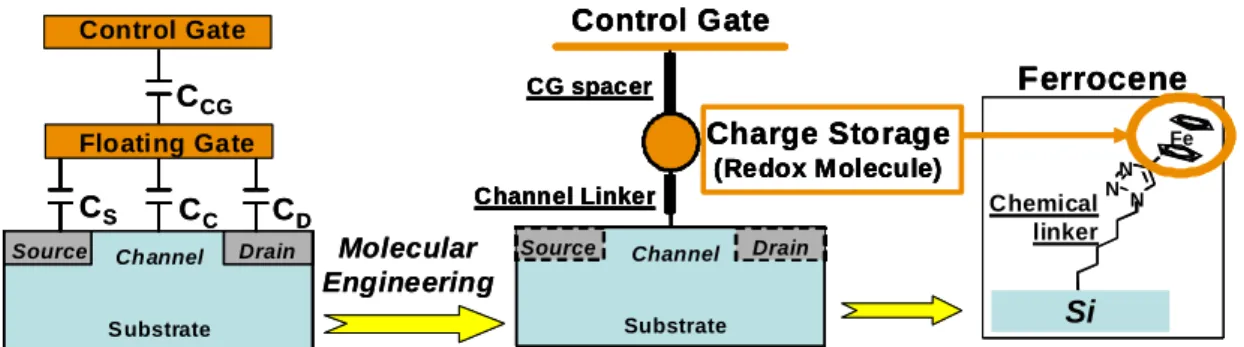
In order to target highly integrated and non-volatile performances, few works also investigated molecular flash like memories [LiC04a-b, Pro09, Pro11]. As pictured on figure I.12
molecular building blocks can be used to mimic the classical floating gate architecture. Indeed, as suggested by Pro et al, redox molecules acting as storage center with very high density of charges (>1013cm-2) could be associated with chemical linker (typically Alkyl chain), replacing the
tunneling oxide and preventing discharge of the molecule for nonvolatile application [Pro11].
Moreover, molecular grafting and self-assembly enable bottom-up approach particularly interesting for nano-scaled fabrication. A demonstration of functional flash like hybrid devices is presented on figure I.13 where porphyrins were grafted on nano-wire transistor enable hysteresis on the transistor characteristics [Li04Cb].
Channel Substrate Source Drain Control Gate Channel Substrate
Source Channel Drain
S ubstrate Source Drain CCG Floating Gate CS CC CD Channel Substrate Source Drain Control Gate Channel Substrate
Source Channel Drain
S ubstrate Source Drain CCG Floating Gate CS CC CD Channel Substrate Source Drain Channel Linker Channel Substrate Source Drain CG spacer Channel Substrate Source Drain Control Gate Charge Storage (Redox Molecule) Channel Substrate Source Drain Channel Linker Channel Substrate Source Drain CG spacer Channel Substrate Source Drain Control Gate Charge Storage (Redox Molecule) Molecular Engineering Channel Substrate Source Drain Channel Linker Channel Substrate Source Drain CG spacer Channel Substrate Source Drain Control Gate Charge Storage (Redox Molecule) Channel Substrate Source Drain Channel Linker Channel Substrate Source Drain CG spacer Channel Substrate Source Drain Control Gate Charge Storage (Redox Molecule) Molecular Engineering N N N Fe Si N N N Fe Si Ferrocene Chemical linker N N N Fe Si N N N Fe Si Ferrocene Chemical linker N N N Fe Si N N N Fe Si N N N Fe Si N N N Fe Si Ferrocene Chemical linker
Figure I.12: Illustration of molecular flash-like memory concept. The conventional floating gate architecture (Left) consists in a charge storage center with a channel linker and controlled by the gate polarization (Central picture). With molecular approach this could be practically realized by using Redox molecules grafted on the substrate (Right) [Pro11].


![Figure I.7: Overview on emerging memory classification suggested by International Technology Roadmap for Semiconductors [ITRS10, Jeong11]](https://thumb-eu.123doks.com/thumbv2/123doknet/12896094.370987/28.892.142.758.267.649/overview-emerging-classification-suggested-international-technology-roadmap-semiconductors.webp)
![Figure I.9: Comparison of memory performance for the main emerging technologies [Numonyx09]](https://thumb-eu.123doks.com/thumbv2/123doknet/12896094.370987/29.892.182.715.639.886/figure-comparison-memory-performance-main-emerging-technologies-numonyx.webp)
![Figure I.10: Evolution of storage hierarchy in computing architecture where Resistive RAM could be employed for the Storage Class Memory application [Lam09]](https://thumb-eu.123doks.com/thumbv2/123doknet/12896094.370987/30.892.214.690.222.492/evolution-hierarchy-computing-architecture-resistive-employed-storage-application.webp)