Degradation Study of AIGaN/GaN HEMT through
Electro-Thermo-Mechanical Calculations and
Thermo-Reflectance Measurements
by
Feng Gao
B.S., Physics (2008) Fudan University MA SSAcHUSETTS INSTITUTE OF TECHNOLOGYNOV 19 2010
LIBRARIESSubmitted to the Department of Materials Science and Engineering in Partial Fulfillment of the Requirements for the Degree of
Master of Science in Materials Science and Engineering at the
Massachusetts Institute of Technology August 2010
@2010 Massachusetts Institute of Technology All rights reserved
r
U Department of Materials Science and Engineering
August 13, 2010
Certified by
And
Tomes Palacios Associate Professor of Electrical Engineering Thesis Supervisor
' ari V. Thompson
Professor of Materials Science and Engineering
Thejsis ader
unnstopher Schuh Chair, Departmental Committee on Graduate Students Accepted by
ARCHIVES
Acknowledgment
First of all, I would like to express my deepest gratitude to my thesis advisor, Prof. Tomas Palacios. He is one of the most energetic, smartest and kindest people I have ever known. It is my great fortune to join his group and be his student. During these two years, I learned a lot from him not only the knowledge of my research but also the characteristics of being a successful person. I always remember his encouragement when I got frustrated, 'You came to MIT to be the world expert in research. You have the greatest potential to provide the best work!' Had it not been his great guidance to my research and considerable support to my life, I would have never finished this thesis.
Secondly, I would like to thank all my labmates: Bin Lu, Omari Saadat, Han Wang, Will Chung, Allen Hsu, Mohamed Azize, Kevin Ryu, Daniel Piedra and Benjamin Mailly for all the help and advice to my research. They are always good resource for ideas and discussions. In addition, I would like to thank my collaborator Katey Lo in Prof. Rajeev Ram's group for all her great help in my experiment setup and measurements. I also like to thank my thesis reader, Prof. Carl Thompson for giving me invaluable advice and suggestive comments in my thesis.
Last but not least, I would like to share this thesis with my parents. Without their warming support and encouragement, I can hardly make it done. I love you from the bottom of my heart.
This work was made possible by the DRIFT MURI project by the Office of Naval Research and
Degradation Study of AIGaN/GaN HEMT
through Electro-Thermo-Mechanical Calculations
and Thermo-Reflectance Measurements
by
Feng Gao
Abstract
During the last few years, AIGaN/GaN high electron mobility transistors (HEMTs) have been intensively studied for high frequency high power applications. In spite of this great interest, device reliability is still an important challenge for the wide deployment of AIGaN/GaN HEMT technology. To fully understand reliability in these devices, it is necessary to consider the
electrical, mechanical and thermal properties of the operating AIGaN/GaN transistors. Since AIGaN and GaN are both piezoelectric materials, the coupling among electric field, lattice heating and mechanical characteristics gives rise to large changes in strain field and elastic energy density in the transistors under the pinch-off conditions. Most previous work have studied the inverse piezoelectric effect on device degradations, however, quantitative analysis of this failure mechanism is still needed. In this thesis, we have developed the first fully-coupled electro-thermo-mechanical simulation of AIGaN/GaN HEMTs to study the correlation between the critical voltages of the gate current degradation and the lattice temperature distributions of these devices under the reverse-gate-bias reliability testing. In addition, we have compared the numerical results of our simulations with DC measurements and high resolution thermo-reflectance images, obtaining excellent agreement for both of them. Moreover, our studies suggest a covenient and low-cost way to obtain the reliability characteristics of AIGaN/GaN HEMTs by using the thermo-reflectance measurements of the lattice temperature distributions for those devices.
Content
CHAPTER 1 INTRODUCTIO N ... 5
1.1 INTRODUCTION OFALGAN/GAN HEM Ts... 5
1.2 BACKGROUND AND M OTIVATION OF RELIABILITY STUDIES ... 7
1.3 THESIS OUTLINES ...---... 9
CHAPTER 2 SELF-CONSISTENT ELECTRO-THERMAL SIMULATIONS... 11
2.1 INTRODUCTION ...--- 11
2.2 BASIC SEMICONDUCTOR PHYSICS ... 11
2.2.1 Poisson's Equation ... 11
2.2.2 Carrier Continuity Equations...12
2.3 DRIFT-DIFFUSION M ODEL... 12
2.3.1 Drift-Diffusion Transport Equations ... 13
2.4 LATTICE HEATING M ODEL ... 14
2.4.1 Lattice Heat Flow Equation ... 14
2.4.2 M odified Drift-Diffusion Equations ... 15
2.4.3 Heat Generation Equations...15
2.4.4 Therm al Boundary Conditions ... 16
2.5 M OBILITY M ODEL ... 17
2.5.1 Low Field M obility M odel of AIGaN/GaN HEIMTs ... 18
2.5.2 High Field M obility M odel of AIGaN/GaN HEM Ts... 19
2.6 SIMULATION RESULTS ... 20
2.6.1 Transistors Structures ... 21
2.6.2 IV Curves...21
2.6.3 Electric Field Distribution ... 22
2.6.4 Lattice Tem perature Distribution... 25
2.7 SUMMARY ... 26
CHAPTER 3 THERM O-REFLECTANCE M EASUREM ENTS... 27
3.1 INTRODUCTION ... 27
3.2 THEORY...--.- .. 27
3.3 EXPERIMENTAL SETUP ... 28
3.4 EXPERIMENTAL RESULTS... 29
3.4.1 Calibration of Thermo-Reflectance Coefficient... 29
3.4.2 Lattice Tem perature Distribution ... 31
3.4.3 Experim ent vs. Sim ulation ... 38
3.5 DISCUSSION ...--- 40
3.6 SUMMARY ...---..---..---- 41
CHAPTER 4 PIEZOELECTRIC-THERM AL CALCULATIONS... 42
4.1 INTRODUCTION ... 42
4.2 THEORY... 42 3
4.2.1 Fundam ental Equation...42
4.2.2 Equati ons of State ... 43
4.2.3 Alternative Form ulation ... 44
4.2.4 M aterial Properties ... 45
4.2.5 Constitutive Relations ... 48
4.2.6 Equilibrium Equations ... 53
4.2.7 The Boundary Conditions Problem ... 54
4.2.8 Elastic Energy Density ... 55
4.3 CALCULATION RESULTS... 57
4.3.1 Strain ... 57
4.3 .2 Stress ... 60
4.3.3 Elastic Energy Density ... 62
4.4 SUMMARY ... 63
CHAPTER 5 REVERSE-GATE-BIAS RELIABILITY TESTING ... 64
5.1 INTRODUCTION ... 64
5.2 STRUCTURE OF TESTED TRANSISTORS ... 64
5.3 CALIBRATION OF THERMO-REFLECTANCE COEFFICIENT ... 65
5.4 DC M EASUREMENTS OF GATE CURRENT DEGRADATION ... 65
5.5 THERMO-REFLECTANCE M EASUREMENTS OF DEGRADATION... 67
5.6 DISCUSSION ... 70
5.7 SUMMARY ... 72
CHAPTER 6 CONCLUSIONS AND FUTURE W ORK ... 73
6.1 CONCLUSIONS ... 73
6.2 FUTURE W ORK ... 74
INTRODUCTION
1.1 Introduction of AlGaN/GaN HEMTs
GaN-based high electron mobility transistors (HEMTs) have thrived since their first demonstration in 1993 [1]. In less than 20 years, they have evolved from devices with less than 20 mA/mm of output current and virtually no high-frequency performance, to devices with extremely high output power 900W at 2.9GHz and 81W at 9.5GHz, high frequency fT = 225 GHz at Lg = 60nm, high-power efficiency PAE = 75% at Psat = 100W, broadband operation 1.0-2.5 GHz with 50% efficiency [2] and world-wide commercialization since 2004 [3-6].
The great development and extraordinary performance of GaN-based because of the outstanding electronic properties of AIGaN/GaN structures.
Characteristic Silicon AIGaAs/ nAlAs/ SiC
________________
IInGaAs
IlnGaAsI Bandgjap (eV) Electron Mobility at 300K (cm2! Vs) 1.1 1500 1.42 8500 1.35 5400 3.26 700 HEMTs is mainly1500-Saturated (peak) Electron 1.0 1.3 1.0 2.0 1.3
Velocity (x107 cm/s) (1.0) (2.1) (2.3)
(2.0) (2.1)
Critical Breakdown Field 0.3 0.4 0.5 3.0 3.0
(MV/cm)
Thermal Conductivity 1.5 0.5 0.7 4.5 >1.5
(W/cm-K) 15..75.
Table 1.1
As shown in the Table 1.1, AIGaN/GaN structure has high electron mobility (>1500 cm2N*s at
room temperature) and high electron velocity (-2.5x1 07cm/s peak velocity and -1.3x10 7cm/s saturated velocity). In addition, strong piezoelectric and spontaneous polarization in Ill-nitride materials results in a high sheet carrier density (normally 0.7-1.4*1013 cm-2) in AIGaN/GaN
hetero-structure without any conventional doping. The high electron mobility and carrier ...
... .. ... I .. ... ... ... .... ... .. ....
, , ,., 6
hetero-structure without any conventional doping. The high electron mobility and carrier concentration of AIGaN/GaN HEMTs allow the fabrication of these devices with maximum drain current densities in excess of 2 A/mm [7].
On the other hand, as a result of the wide band-gap (-3.49 eV) and high breakdown electric field (>3 MV/cm) of AIGaN/GaN structure, GaN-based HEMTs have very large breakdown voltage (8300V in [8]). Both high current density and large breakdown voltage are important requirements for power amplifiers. Moreover, the high electron velocity makes this material system one of the best candidates for very high frequency operation.
*Miary 100
10
saN
0.1 2 GHz 10 GHz 30 GHz 60 GHz Frequency BandFigure 1.1-1: Important potential applications for GaN-based power transistors
Figure 1.1 summarizes some of the multiple commercial and military applications that could benefit from the use of AIGaN/GaN HEMTs as power devices. As shown above, these transistors can be used in many applications requiring high frequency and high power operations. At lower frequencies, AIGaN/GaN HEMTs are being pursued for power-switching applications [9] and even for biological [10] and chemical/physical sensors [11]. At higher frequencies, the performance of AIGaN/GaN HEMTs has been evolving very fast over the last 20 years. A maximum current gain cut-off frequency (fT) of 163 GHz was reported in AIGaN/GaN HEMTs with a gate length in the 60-90 nm range [12]. When biased for maximum
power gain, these devices could reach 230 GHz of maximum power gain cut-off frequency
(fmax) [13].
The last 20 years has also witnessed the great progress of the output power and power added efficiency (PAE) in GaN devices as power amplifiers. Currently, AIGaN/GaN HEMTs have been already commercially available for power amplification in cell-phone base stations at
2GHz and a total output power in excess of 280W have been reported at that frequency [14]. At 4GHz, AIGaN/GaN HEMTs have demonstrated more than 32 W mm' of output power with a PAE of 54.8% at Vds=120V [15]. This performance is more than one order of magnitude better than those of any other competing semiconductor technology such GaAs and InP.
1.2 Background and Motivation of Reliability Studies
While GaN-based HEMTs are routinely presenting excellent performance, the greatest challenge for the wide deployment has been, and remains, achieving a high level of reliability
and stability concurrently with high-performance operation [16].
First of all, improvements in reliability require a better understanding of the failure mechanisms
of GaN-based HEMTs. Years of research into this area have identified the following major
degradation modes, which can represent the peculiarities of the physics of GaN devices, the
imperfection of the materials and the stability of the fabrication processes:
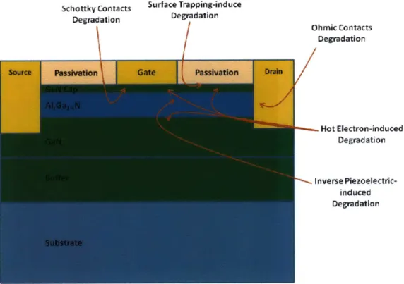
" Schottky and Ohmic Contacts Degradation
* Surface Trapping-induced Degradation * Hot Electron-induced Degradation
* Inverse Piezoelectric-induced Degradation
These four failure modes are also schematically demonstrated in a cross section of a typical AIGaN/GaN HEMT in the figure below, identifying critical areas which can be subjected to the
Schottky Contacts Surface Trapping-induce Degradation Degradation Ohmic Contacts Degradation Hot Electron-induced Degradation Inverse Piezoelectric-induced Degradation
Figure 1.2-1: Schematic cross section of an AIGaN/GaN HEMT. Critical areas subjected to degradation are identified by arrows.
Although the 'gate sinking' resulting from the unstable Schottky contacts was identified as one of the major failure mechanisms of GaAs MESFETs and HEMTs, the Schottky contacts on GaN appear to be normally stable and no 'gate sinking' effect of DC bias has been reported until now, despite of some findings of changes in the Schottky barrier height after some thermal treatments [17],[18]. For the ohmic contacts, minor degradation with less than 2% variation of fresh condition was found during a 2000-h thermal storage test in the nitrogen atmosphere at 340*C [19]. A more systematic study of the stability of the Schottky and ohmic contacts is still needed, but this kind of degradation is much more moderate compared to the others.
Surface trapping-detrapping of electrons at surface states has been suggested as a possible mechanism responsible for the RF current slump and dispersion, which lead in changes of the maximum drain current and knee voltage resulting in reduced power and gain. This kind of trapping can compensate part of the surface component of the spontaneous polarization
.
..........- I I I -I - - .1 ............... .
working as a 'virtual gate' between the actual gate and drain, and hence reduce the 2DEG electron concentration [20].
Another well-know failure mechanism of GaAs-based devices is the hot electron-induced device aging [21],[22], which has also been invoked to explain the current collapse and gate-lag effects in GaN-based HEMTs. There are many excellent work reviewing on this topic, especially those working on the characterization of hot-electron effects by the electroluminescence (EL) microscopy [23].
In this thesis, we study in detail the degradation due to inverse piezoelectric effect. Since the uniqueness of the GaN-based HEMTs, high vertical electric field is created at the drain edge of the gate, which would be seen in our simulations and measurements later. When the electric field or the applied voltage reach a critical value, the gate leakage current starts to jump resulting from the trap generations. And eventually strain relaxation and crystallographic defect formation take place in the device layers. A specific hypothesis relating to the inverse piezoelectric effect has been recently formulated by some authors [24],[25], however, an accurate and complete understanding of the physics behind this degradation mechanisms is still needed. In this thesis, we present a simulation, modeling and measurement framework for the purpose of studying this piezoelectric induce degradation. We have also identified
thermo-reflectance measurements is a powerful technique to evaluate device reliability.
1.3 Thesis Outlines
The thesis is organized in the following way:
In Chapter 2, we develop self-consistent electro-thermal simulations of GaN-based HEMTs in order to estimate the electric field and lattice temperature of two types of fabricated devices. The simulated and measured IV curves of those devices are compared to evaluate the
In Chapter 3, we use for the first time thermal-reflectance measurements of the surface lattice temperature of the AIGaN/GaN HEMTs to test the accuracy of the thermal part of the simulations developed in Chapter 2. The experimental results of the peak lattice temperature match the previous simulation data very well. Moreover, we found an interesting feature of the thermal-reflectance measurements that could be used as an easy and fast tool for the reliability testing of the AIGaN/GaN HEMTs.
In Chapter 4, with the simulation data of the electric field and lattice temperature obtained in Chapter 2 and verified in Chapter 3, we established a new piezoelectric-thermal model for the calculations of the mechanical characteristics such as strain, stress and elastic energy density in the AIGaN layer of a HEMT under various bias conditions, which are very important for the prediction of the reliability in the failure modes of the inverse piezoelectric-induced degradation. In Chapter 5, we use thermo-reflectance measurements to study device degradation as a function of reverse-gate-bias step stress.
SELF-CONSISTENT ELECTRO-THERMAL SIMULATIONS
2.1 Introduction
Through decades of research in semiconductor physics, a basic set of equations and models has been developed to understand and predict the performance of semiconductor devices including GaN-based HEMTs [26]. The commercial software Silvaco Atlas is a device simulator which incorporate many of these equations [27], and we have used it to simulate the electrical and thermal characteristics of the AIGaN/GaN transistors we fabricated in lab to obtain the electric field and lattice temperature distributions in the cross section of the devices and to analyze key features in the AIGaN layer that will be investigated in the latter chapter.
2.2 Basic Semiconductor Physics
In this section, the basic equations used by our device simulator are reviewed.
2.2.lPoisson's Equation
Poisson's equation is one of the most fundamental equations in the theory of semiconductor devices [26]. It has the following form:
div(EV y/) = -p (2.2.1-1)
where tp is the electrostatic potential, E is the local permittivity and p is the local space charge density. Poisson's equation relates the electrostatic potential to the space charge density. The reference potential can be defined in various ways. For the software Silvaco Atlas that we are using in the thesis, the reference potential is always the intrinsic Fermi potential of the device [27].
2.2.2 Carrier Continuity Equations
The carrier continuity equations are another set of fundamental equations of device physics which have the following simple and very intuitive forms [26]:
oh 1
-=-div , + G - R (2.2.2-1)
q
-divJP,+ G, - R, (2.2.2-2)
where n and p are the electron and hole concentration, Jn and Jp are the electron and hole current densities, Go and Gp are the generation rates for electrons and holes, Ra and Rp are the recombination rates for electrons and holes.
Carrier continuity equations connect the carrier concentration to the carrier current densities and generation-recombination rates, offering an important link to the device performance.
2.3 Drift-Diffusion Model
Poisson's equation and carrier continuity equations provide the general framework for semiconductor device simulations. But they are not sufficient to simulate devices. Further secondary equations are needed to specify particular models for current densities and generation-recombination rates.
The current-density equations, or charge transport models, are usually obtained by applying approximations and simplifications to the Boltzmann transport equation [28]. Those assumptions can result in a number of different transport models such as the drift-diffusion model, the energy balance transport model or the hydrodynamic model.
In this thesis, we use the simplest model of charge transport, the drift-diffusion model, which is accurate enough for our simulations of the electrical characteristics of GaN-based transistors.
As we will see in the later part of this chapter, excellent agreement between simulations and
experiments have been obtained.
2.3.1 Drift-Diffusion Transport Equations
In the framework of the drift-diffusion model [28], the current densities are expressed in terms of the quasi-Fermi levels On and Op as the following:
Jn = -qpnnV #n (2.3.1-1)
JP = -qp pV #, (2.3.1-2)
where pn and pp are the electron and hole mobilities. The quasi-Fermi levels On and Op are linked to the carrier concentrations and the potential through Boltzmann approximations:
n = n i, exp kTL
-2313
p = ni, exp (2.3.1-4)
_ k
TL-where nie is the effective intrinsic concentration, TL is the lattice temperature and tp is the
electrostatic potential. These two equations can be re-written to define the quasi-Fermi potentials: kT n , = V_ TL in (2.3.1-5) q nie O, - V k in p (2.3.1-6) q ni
By substituting these equations into the equation 2.3.1-1 and the equation 2.3.1-2, the following conventional formulas of the drift-diffusion transport equations are obtained:
kT
J= qnpE +qDVn 5n V (2.3.1-7)
q
J, = qppE, -qDVp, Z, =-V(v_ kL Ine(2318)
q
If we are not considering the lattice heating effect, we just set the local lattice temperature as constant e.g. 295K, and self-consistently solve the three sets of equations (Poisson's equation, carrier continuity equations and drift-diffusion transport equations) under specific device
domains and structures, to get all of the electrical characteristics such as electrostatic potential, electric field, current densities, etc in the device.
Although these simulations results match the measurements quite well under low bias conditions, at higher bias, as the lattice heating plays a more and more important role to the electrical performance of the real device, this model becomes inaccurate (see the black dashed line in Figure 2.6.2-1 and 2.6.2-2 in the latter section). In addition, these simulation results do not include any data on the lattice temperature of the device, which will be heavily used in our further calculations in the latter chapters. So, it is necessary to introduce another two important models: lattice heating model and mobility model into our simulations.
2.4 Lattice Heating Model
Silvaco Atlas allows us to calculate the lattice temperature distributions in semiconductor devices using its lattice heating model [27]. This model consists of several sets of heat-transfer related equations, which can be combined with the drift-diffusion model for self-consistent simulations.
2.4.1 Lattice Heat Flow Equation
The first fundamental equation of the lattice heating model is the intuitive lattice heat flow equation:
C = V(V TL)+ H (2.4.1-1)
And in the steady state:
V(KVTL) + H = 0 (2.4.1-2)
where C is the heat capacitance per unit volume, K iS the thermal conductivity, H is the heat
2.4.2 Modified Drift-Diffusion Equations
In the framework of the lattice heating model, the electron and hole current densities are modified to account for the spatially varying lattice temperatures:
J= -qn(V, +PVTL) (2.4.2-1)
J, = -qpp(V$, + PVTL) (2.4.2-2)
where Po and Pp are the absolute thermoelectric powers for electrons and holes. Conventionally, Pn and Pp are modeled as follows [27]:
k n 3
q N, 2
P (ln - ) (2.4.2-4)
For simplicity and fast convergence of the simulation, in this thesis we will just use the normal drift-diffusion equations as the equations 2.3.1-7 and 2.3.1-8.
2.4.3 Heat Generation Equations
When carrier transport is handled in the drift-diffusion model, the heat generation term, H, has the following form:
H =q" +q " -qT(J,,VP,))+qTL JpVP p)+q(R -G)[TL bnJ (
pann p p -IT -)& P
-qTL I rd + Pn ]divJn -qTL + p
n,p n,p
and in the steady state, the current divergence can be replaced with the net recombination. Equation 2.4.3-1 then simplifies to:
H=[q +q +q(R-G)[p, -, p+TL (Pp (2.4.3-2)
lnn lpp
In the above equation, the heat generation could be separated into three terms, each of which has its own physical meaning:
" q +q is the Joule heating term;
lnn ppp
* q(R - G)[#, - n+ TL (P -Pn)] is the recombination-generation heating and cooling term;
* -qTL(JnVPn +JPVPp)is the term of the Peltier and Thomason effects.
In our simulations, also for the reason of easy and fast convergence, we only calculate the Joule heating term for the heat generation. This term can be re-written in a simpler and form as follows:
H = (Jn + J,) - E (2.4.3-3)
2.4.4 Thermal Boundary Conditions
To solve the lattice heat flow equation in the device domain, the thermal boundary conditions must be specified:
(2.4.4-1)
where a is either 0 or 1, Jtot is the total energy flux and s is the unit of the external normal of the boundary.
The projection of the energy flux onto s is:
(2.4.4-2)
When a=0, equation 2.4.4-2 specifies a Dirichlet boundary condition (fixed boundary temperature).
In this thesis work, we use Dirichlet boundary condition for all thermal simulations, which implies that we set the bottom of the device substrate at fixed room temperature 295K.
( J,,, 5) a(T - T,)t
(J -i) L + (TLpn + On)jn + (TLpp + Op)jp
2.5 Mobility Model
Electrons and holes are accelerated by electric fields, but lose momentum as a result of various scattering processes. These scattering mechanisms include lattice vibrations (phonons), impurity ions, other carriers, surfaces, and other material imperfections. Since the effects of all of these microscopic phenomena are lumped into the macroscopic mobilities introduced by the transport equations, these mobilites are therefore functions of the local electric field, lattice temperature, doping concentration, and so on.
Mobility modeling is normally divided into two areas: * Low field behavior
* High field behavior
The low electric field behavior has carriers almost in equilibrium with the lattice and mobility has a characteristic low-field value that is commonly denoted by the symbol Pno,po. The value of this mobility is dependent on phonon (lattice temperature) and impurity scattering (impurity concentration), both of which act to decrease the low field mobility.
The high electric field behavior shows that the carrier mobility declines with the electric field because the carriers that gain energy can take part in a wider range of scattering processes. The mean drift velocity no longer increases linearly with the increasing electric field, but rises more slowly. Eventually, the velocity does not increase any more with the increasing field but otherwise drops and at the end it saturates at a constant velocity. This constant velocity is commonly denoted by the symbol vsat. This behavior can be well modeled by the Monte Carlo Simulations shown in the Figure 2.5-1 below:
x
2.5- Velocity Saturation Model of AIGaN/GaN HEMTs e 0.5 @T=300K 0' 0 0.2 0.4 0.6 0.8 1 1.2 1.4 1.6 1.8 2
Lateral Electric Field (MV/cm)
Figure 2.5-1: Monte Carlo simulations of the electron velocity in AIGaN/GaN HEMTs as a function of the lateral electric field [29].
2.5.1 Low Field Mobility Model of AlGaN/GaN H EMTs
Based on the Monte Carlo simulations [29], the general expression for the low field mobility of AIGaN/GaN transistors used in the drift-diffusion simulations can be fitted :
yo(TL,N) =p'in
-~ fl4(2.5.1-1)
where TL is the local lattice temperature and N is the local (total) impurity concentration. The values of a, @1, P2,
13,
04, pmin, Pmax, Nret that we used in out simulations are listed in thefollowing table:
modeled by equation (2.5.1-1) is plotted in the Figure 2.5.1-1:
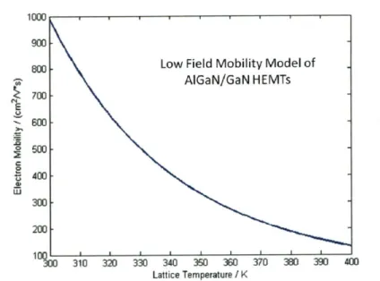
Al3aN/fUaN ritiVi IS ~700 600 o500 e r,400 300 200 310 32 3 3 350 3 370 380 390 400 Lattice Temperature / K
Figure 2.5.1-1: Low field electron mobility in AIGaN/GaN HEMTs as a function of the lattice temperature.
From the figure above, we can see that the low field electron mobility in GaN drops from -1000 cm2N*s to -130 cm2N*s as the lattice temperature increases from 300K to 400K.
2.5.2 High Field Mobility Model of AlGaN/GaN HEMTs
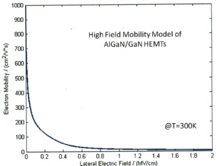
According to the reference [29], the general expression for the high field mobility of AIGaN/GaN transistors used in the drift-diffusion simulations has the following formulation:
o ( T L ,N ) + v a E n -1" E
= n2 E ni (2.5.2-1)
E C) EC
1+
a --
+L-where po(TL,N) is the low field mobility modeled in equation 2.5.1-1, and E is the local electric field. The values of vsat, a, n1, n2, Ec we used in our simulations are listed in the following table:
vsat(10cm I s) a n, n2 E,(kV /cm)
GaN 1.3 7.0 4.5 0.7 215
The high field mobility behavior modeled by the equation (2.5.2-1) is plotted in the Figure 2.5.2-1:
1000
900
800 High Field Mobility Model of
700 AIGaN/GaN HEMTs E 600 500 C 400 e 00 LLI @T=300K 100 0-0 0.2 0.4 0.6 0.8 1 1.2 1.4 1.6 1.8 2
Lateral Electric Field / (MV/cm)
Figure 2.5.2-1: Electron mobility in AIGaN/GaN HEMTs as a function of the lateral electric field at T=300K.
From the figure above, we can see that the high field electron mobility in GaN drops from -1000 cm2N*s to -0 cm2N*s (i.e the electron velocity saturates) as the lateral electric field increases from 0 to 2 MV/cm at 300K.
2.6
Simulation Results
Using the drift-diffusion model, lattice heating model and specific mobility models for AIGaN/GaN HEMTs and correctly setting all of the material parameters including band gap, density of states, electron affinity, permittivity, thermal conductivity, etc., we have simulated the electric field and lattice temperature distribution. There is a lot of excellent work in the literature regarding the simulations of the electrical performance of AIGaN/GaN HEMTs [30] [31], but very little on the simulations of the thermal performance [32]. Therefore, this chapter of the thesis focuses mainly on the lattice temperature simulations of the AIGaN/GaN transistors. It
also discusses the electrical performance of the devices to test the accuracy of the physical models used.
... .... .... ...
2.6.1 Transistors Structures
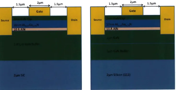
The simulated transistors have exactly the same structures of our real AIGaN/GaN HEMTs, which were fabricated following our standard technology. In order to investigate into the effect of different substrates on the lattice temperature distribution in the device, we fabricated the same AIGaN/GaN HEMTs structures on SiC (transistor A) and Silicon substrates (transistor B) respectively. The following figures show the structures of our two types of transistors:
2pim 2pm
Figure 2.6.1-1: Schematic structure of Transistor A Figure 2.6.1-2: Schematic structure of Transistor B
2.6.2 IV Curves
The DC current measurements and the simulation data of Transistor A and Transistor B are shown in the Figure 2.6.2-1 and 2.6.2-2. We can see that the experimental and simulated IV curves of both transistors are in perfect agreement and a clear difference between using
models with and without lattice heating models (black dashed lines).
- experimert ... -- simulation
T sLattice heating effect 600 T ransistcirA I
E
02
3W 6 7 8 9 1
Vds I V
Figure 2.6.2-1: Measured (dot) and simulated (solid line) IV curves of transistor A. The black dashed line indicates the calculated IV curve at Vgs=2V without lattice heating models.
~2W ISO 100 50 1 2 3 4 5 6 7 8 9 10 Vd i V
Figure 2.6.2-2: Measured (dot) and simulated (solid line) IV curves of transistor B. The black dashed line indicates the calculated IV curve at Vgs=2V without lattice heating models.
From the IV curves above, we also find that the drain-to-source current of Transistor A is larger than in Transistor B. This is because of the better quality and lower defects densities of the sample grown on the SiC substrate, which create fewer buffer traps than in the sample grown on the Silicon substrate.
The excellent agreement between the experiment and simulation results of the DC performance of the AIGaN/GaN HEMTs provide a strong proof of the accuracy of the physical models we are using in the simulations and also validate the framework of the self-consistent electro-thermal method used to simulate the electric field and the lattice temperature distribution in the AIGaN/GaN HEMTs, both of which are much more difficult to measure in reality.
2.6.3 Electric Field Distribution
The vertical and lateral electric fields across the device in the AIGaN lattice above the channel are extracted from the simulation data for both transistors:
- ---Vg=V Vd=12V VpfWVVds=15
2 ---Vgs=0Vs=15y
1C' 1.5
0.5 L
Source Gate Drain
0 1 15 2 26 3 36 4 45
Microns
Figure 2.6.3-1: Simulation of the vertical electric field along the AIGaN layer of transistor A under increasing
drain-to-source bias at Vgs=OV.
- vgs=uy vOs-Ie
--- Vgs=OVVds=15V 2- -Vg s4Vd s-1I8V
5
Source Gate _ _ Drain
W5 1 15 2.5 3 3.5 4 4.5
Microns
Figure 2.6.3-2: Simulation of the vertical electric field along the AIGaN layer of transistor B under increasing drain-to-source bias at Vgs=OV.
1 1.5 2 2.5 Microns
0.68
3 3.5 4 4.5 W5S 1 1,5 2 2.5
Microns 3 3.5 4 4.5 Figure 2.6.3-3: Simulation of the lateral electric field
along the AIGaN layer of transistor A under increasing drain-to-source bias at Vgs=OV.
Figure 2.6.3-4: Simulation of the lateral electric field along the AIGaN layer of transistor B under increasing drain-to-source bias at Vgs=OV.
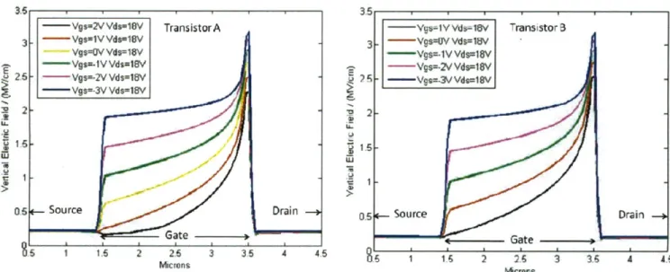
23 i 2 -o I1 0 3 0.4 - Vgs-OV Vdsw3V TransistorA - - Vgs=VVds=6V Vgs=0V Vds=9V - Vgs=cV Vds=12V -- Vgs=0V Vds-15V - Vg=V Vd=18V
e- Source Gate : Drain -,
-Vgt=V Vds=3V Transistor B -- Vgs=V Vds=6V Vs=0V Vds=9V -- Vgs=OV Vds=12V - Vgs=V Vds=15V - Vgs9OVds=1V
4 Source : Gate - 0 Drain -+
I. ~
2.5 -Vg-2V Vds=16V
- Vgs=-3V Vds=18V
.
.
w
0-6os-- Source Drain
Gate
5 1 1.5 2 2.6 3 3.5 4 4.5 Microns
Figure 2.6.3-5: Simulation of the vertical electric field along the AIGaN layer of transistor A under decreasing gate-to-source bias at Vds=18V. - Vgs=2V Vds=18V TransistorA Vgs-lVVds18V 1.6 Vgs=OV Vds=18V VgS-1VVds=18V 14 - V_-2VVds=18V 12 -Vgs-3V Vds=18V 0.6 0.4
0.2 Source Gate Drain
WS 1 1.5 2 2.5 3 3.5 4 45 Microns
Figure 2.6.3-7: Simulation of the lateral electric field along the AIGaN layer of transistor A under decreasing gate -to-source bias at Vds=1 8V.
7 --- Vgs-3VVde=18V .5 0.5 S- Source Drain Gate
B6
1.6 2 2.6 3 3' A 46 MicrorsFigure 2.6.3-6: Simulation of the vertical electric field along the AIGaN layer of transistor B under decreasing gate-to-source bias at Vds=1 8V.
0.
i 1A 2 25 3 3.5 A A
Microns
Figure 2.6.3-8: Simulation of the lateral electric field along the AlGaN layer of transistor B under decreasing gate -to-source bias at Vds=18V.
From the figures above, both the lateral and vertical electric fields peak at the drain edge of the gate, rise as the increasing drain-to-source voltage and drop as the decreasing gate-to-source voltage. In addition, the very similar electric field profiles of Transistor A and Transistor B result from the same device scales and structures regardless of the different substrates and defect densities. -- Vgs=VVds1BV Transistor [! Vgs=(V Vds=18V 6 Vg--t V Vds=18V Vgs=-2VVds=18V 4 Vgs--3V Vde-18V 2 6 4
--2.6.4 Lattice Temperature Distribution
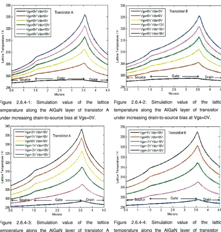
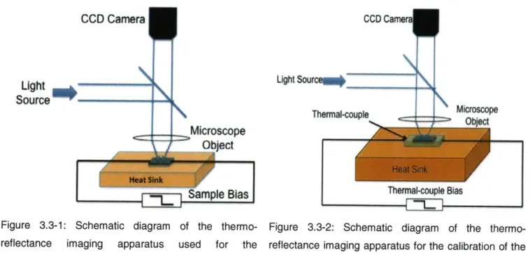
The lattice temperature distributions across the device in the AIGaN layer above the channel are also extracted from the simulation data for both transistors:
3N . I I I 1 330.
315
'310
5 2 25A 3,5 4 45
Microns
Figure 2.6.4-1: Simulation value of the lattice temperature along the AIGaN layer of transistor A
under increasing drain-to-source bias at Vgs=OV.
3Z- Vgs-3VVds-I8V
305 1 1. 2 2. 3 3. 4 45
Microns
Figure 2.6.4-3: Simulation value of the lattice temperature along the AIGaN layer of transistor A
under decreasing gate-to-source bias at Vds=1 8V.
2.5 Microns
Figure 2.6.4-2: Simulation value of the lattice temperature along the AIGaN layer of transistor B under increasing drain-to-source bias at Vgs=OV.
3-310
300- 4 - Gate
05 1 5 2 2.5 3 3.5 4 4.6 Micrers
Figure 2.6.4-4: Simulation value of the lattice temperature along the AIGaN layer of transistor B under decreasing gate-to-source bias at Vds=18V.
In these figures, we also find that the peak lattice temperature happen at the drain edge of the gate for both transistors. The reason for this is that the peak lateral electric field in the channel at the drain edge of the gate generates the highest heat dissipation therefore the highest lattice temperature, as demonstrated in equation 2.4.3-3. Moreover, from the equation 2.4.3-3 and 2.4.1-2, we can see that for the same material (same thermal conductivity), the lattice temperature is proportional to the output power in the device. Therefore, since the current of the Transistor A is larger than that of the Transistor B under the same bias conditions, the
lattice temperature of Transistor A should be larger than that of the Transistor B. However, this is not the case in the figures from 2.6.4-1 to 2.6.4-4, where the lattice temperatures of Transistor A are almost the same as those of Transistor B under the same bias conditions. Actually, this is exactly what we want to see. Due to the fact that the thermal conductivity of
SiC material is nearly four times larger than the thermal conductivity of Silicon material, heat, is therefore more easily dissipated from the device into the substrate for Transistor A, causing the lattice temperatures along the channel drop faster despite of the higher power.
2.7 Summary
In conclusion, by using the commercial software Silvaco Atlas, we successfully modeled and simulated the electrical and thermal characteristics of the standard AIGaN/GaN HEMTs, which were fabricated on wafers with different substrates (SiC and Silicon). The simulated drain current of the devices matches perfectly with the experimental data, and the effect of the substrate on the lattice temperatures in device performance was also simulated in the simulations as expected. To provide more confidence in this self-consistent electro-thermal simulation, the lattice temperatures data generated in this chapter will be compared with the
CHAPTER
3
THERMO-REFLECTANCE MEASUREMENTS3.1 Introduction
Thermo-reflectance microscopy is an important imaging tool for measuring surface temperature distributions [33]. Since it does not require direct physical contact of the surface as opposed to the use of thermocouples, and it offers better spatial resolution than IR (infrared) thermal imaging, and micro-Raman spectroscopy [34], thermo-reflectance microscopy finds
many applications in physics and engineering, such as device failure analysis and design optimization [35].
3.2 Theory
Thermo-reflectance microscopy is based on the fact that the reflectivity of a surface depends weakly on its temperature. To first order, the fractional change in the sample's reflectivity ARIR ( AR refers to the change in reflectivity and R is the total reflectivity) in response to surface temperature variations AT is proportional to AT:
A 1= =R4R 18AR
A T AR (3.2-1)
R oT R R
where
#
is the so-called thermo-reflectance coefficient, a characteristic of the specific material [36] and wavelength of illumination [37]. Knowledge of the material-dependent thermo-reflectance coefficient , which has typical value ranging from 10' to IV K-', enables the calculation of AT from the measured ARIR.3.3 Experimental Setup
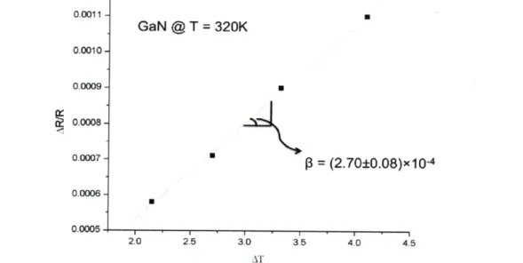
The setup of the thermo-reflectance measurements is schematically shown in the figures below:
CCD Camera CCD Camer
Li Lghth Light Source1
Figure 3.3-1: Schematic diagram of the thermo-ref lectance imaging apparatus used for the measurement of AIGaN/GaN transistor.
Figure 3.3-2: Schematic diagram of the thermo-reflectance imaging apparatus for the calibration of the thermo-reflectance coefficient of the surface material.
A light-emitting diode (LED) is used to illuminate the surface of the tested devices. The reflected LED light is collected through a standard reflectance-mode microscope objective and imaged onto a CCD array with a resolution of 652x400 pixels. An optical spatial resolution of 150±10 nm is obtained using 467nm (blue) LED light, and a 100x, NA=0.8 microscope objective, which is in quantitative agreement with Sparrow's criterion.
The temperature of the sample in Figure 3.3-1 is modulated using a square voltage source of frequency co. The CCD camera then takes images of the sample at a frequency phase-locked to the excitation. To detect the amplitude of Joule heating, the camera takes images of the device at a trigger frequency of 8M, since the temperature change from this heating has a frequency of 2w. In this case the sequential images (each separated by a difference of rr/2 of the phase of the temperature oscillation) are accumulated in 4 image buffers, denoted as 11, 12, 13, and 14. The main quantity of interest is the magnitude normalized change in reflectance R, denoted AR/R, and related to the image buffers by:
28
AR z r (I -1I3)2+(I2_) 2 (3.3-1) R - 2 I, + I2 + I, + 4
Once the ARIR image is obtained, it remains to calibrate the ARIR map to the temperature scale.
The system of calibration is shown in Figure 3.3-2. A flat, uniform sample of the material of interest (GaN cap layer for Transistor A and Transistor B) is placed on a thermo-couple attached with a heat sink (a bulk of copper). The temperature of the thermo-couple (and the sample) is modulated using a square voltage bias. A thermo-reflectance image of the sample is obtained in the above manner. A small thermocouple is used in order to ensure good thermal contact, for fast response time, and to minimize any error in the temperature measurement caused by parasitic heat conduction through the thermocouple wires. A low numerical aperture lens is used to avoid parasitic effects due to sample motion from thermal expansion. The (uniform) thermo-reflectance amplitude is then divided by the amplitude of the temperature oscillation as determined by the thermocouple, giving the thermo-reflectance coefficient
P.
Thermo-reflectance maps of the material can then be easily converted to temperature images.3.4 Experimental Results
In this section of the chapter, the first thermo-reflectance images of AIGaN/GaN HEMTs are demonstrated and analyzed. These high-resolution images (-100nm) of lattice temperature provide a lot of information of the measured device including the important defects densities and distributions, which have. traditionally been very difficult to test.
3.4.1 Calibration of Thermo-Reflectance Coefficient
Based on the fact that different materials have different thermo-reflectance coefficients [36], in order to obtain the lattice temperature maps on the GaN cap layer of Transistor A and
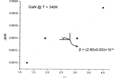
Transistor B, calibration of the GaN surface material is needed. Since the thermo-reflectance coefficient also slightly changes with temperature, we measured the variation of the thermo-reflectivity as a function of the variation of the temperature at 300K, 320K and 340K. The results are shown in the figures below respectively.
0.000s5 -0.00050 -0.00045 -0.00040 - 0.00035-0.00030 -GaN @ T = 300K = (2.64±0.30)x104 ).4 0.6 0.8 1.0 1.2 1.4
Figure 3.4.1-1: Variation of the thermo-reflectivity as a function of the variation of the lattice temperature measured on GaN sample and started with 300K. The slope of the fitting line is the thermo-reflectance coefficient. 0.0011 -0.0010 -0.0009 -0.0008 0.00071 GaN @ T = 320K P = (2.70±0.08)xlO-4 0.0006-0.00051 ,T I 2.0 2.5 3.0 3.5 4.0 4.5 AT
Figure 3.4.1-2: Variation of the thermo-reflectivity as a function of the variation of the lattice temperature measured on GaN sample and started with 320K. The slope of the fitting line is the thermo-reflectance coefficient.
0.0020 GaN @ T = 340K a 0.0018- 0,00160.0014 -0.0012 -f = (2.80±0.83)x104 0.0010 -1.0 1.5 2.0 2.5 3.0 3.5 4.0 \T
Figure 3.4.1-3: Variation of the thermo-reflectivity as a function of the variation of the lattice temperature measured on GaN sample and started with 340K. The slope of the fitting line is the thermo-reflectance coefficient.
We find that the linear relationship of AR/R and AT holds well for the temperature rages of
interest and the thermo-reflectance coefficient varies very little (<10%), which gives us an error of less than 2% (-5K) in ternerature. Jherefore, it is statistically reasonable to treat the average thermo-reflectance coefficient measured by the calibration as the theoretical one involved in the temperature calculation. By averaging the data above, we obtain a thermo-reflectance coefficient of 2.73x1 0-4 K-1 for GaN material under the 467nm (blue) LED light. 3.4.2 Lattice Temperature Distribution
Using the reflectance coefficient obtained in the calibration and converting the thermo-reflectivity maps into lattice temperature, we obtained accurate data for the lattice temperature distribution on the GaN cap layer of Transistor A and Transistor B.
Figures 3.4.2-1 to 3.4.2-12 show the lattice temperature profiles of Transistor A and Transistor B from Vds=3V to Vds=1 8V (step 3V) at Vgs=OV. The scales of the GaN cap layer bands in each image are 1.5 pm wide and 40 pm long and the resolution is about 150 nm.
Transistor A
Drain
Figure 3.4.2-1: Top view of the lattice temperature distribution on the GaN cap layer of Transistor A at Vgs=OV, Vds=3V.
I
DrainI
Figure 3.4.2-3: Top view of the lattice temperature distribution on the GaN cap layer of Transistor A at Vgs=OV, Vds=6V.
I
Drain TVmpr"*- / K :5 3M0 326 320 316 310 3M5 3M6 9mper1ure/ K 3A5 340 3315 30 326 320 316 1U 206 ' erx/ K 346 3410 336 3M0 326 X20 310 306 3011) 295Figure 3.4.2-5: Top view of the lattice temperature distribution on the GaN cap layer of Transistor A at Vgs=OV, Vds=9V.
Transistor B
Drain
Figure 3.4.2-2: Top view of the lattice temperature distribution on the GaN cap layer of Transistor B at Vgs=OV, Vds=3V.
Drain
Gate
Source
Figure 3.4.2-4: Top view of the lattice temperature distribution on the GaN cap layer of Transistor B at Vgs=OV, Vds=6V.
Drain
Figure 3.4.2-6: Top view of the lattice temperature distribution on the GaN cap layer of Transistor B at Vgs=OV, Vds=9V.
Drain
Gate
Source
Figure 3.4.2-7: Top view of the lattice temperature distribution on the GaN cap layer of Transistor A at Vgs=OV, Vds=1 2V.
Drain
Gate
Source
Figure 3.4.2-9: Top view of the lattice temperature distribution on the GaN cap layer of Transistor A at Vgs=OV, Vds=1 5V.
Drain
Source
Figure 3.4.2-11: Top view of the lattice temperature distribution on the GaN cap layer of Transistor A at Vgs=OV, Vds=1 8V. 1Umpeture/ K 3A" 340 336 3130 326 320 310 306 3'46 340 316 310 306 T Jvcab 340 326 320 315 30 300 I Drain
Figure 3.4.2-8: Top view of the lattice temperature distribution on the GaN cap layer of Transistor B at Vgs=OV, Vds=12V.
I
DrainFigure 3.4.2-10: Top view of the lattice temperature distribution on the GaN cap layer of Transistor B at Vgs=OV, Vds=15V.
I
Drain
Figure 3.4.2-12: Top view of the temperature distribution on the GaN cap Transistor B at Vgs=OV, Vds=1 8V.
lattice layer of
Figures 3.4.2-13 to 3.4.2-23 below show the lattice temperature profiles of Transistor A and Transistor B from Vgs=2V to Vgs=-3V (step -1 V) at Vds=1 8V. The dimentsions of the GaN cap layer bands in each image are also 1.5 pm wide and 40 pm long and the resolution is still about 150 nm.
Transistor A
Drain
Gate
Source
Figure 3.4.2-13: Top view of the lattice temperature distribution on the GaN cap layer of Transistor A
at Vgs=2V, Vds=1 8V.
Drain
Gate
Source
Figure 3.4.2-14: Top view of the lattice temperature distribution on the GaN cap layer of Transistor A at Vgs=1V, Vds=1 8V.
Drain
Gate
Source
Figure 3.4.2-1.5: Top view of the lattice temperature distribution on the GaN cap layer of Transistor A at Vgs=0V, Vds= 18V.
Drain
Gate
Source
Figure 3.4.2-16: Top view of the lattice temperature distribution on the GaN cap layer of Transistor A at Vgs=-1V, Vds=1 8V.
Drain
Gate
Source
Figure 3.4.2-17: Top view of the lattice temperature distribution on the GaN cap layer of Transistor A at Vgs=-2V, Vds=1 8V.
Drain
Gate
Source
Figure 3.4.2-18: Top view of the lattice temperature distribution on the GaN cap layer of Transistor A at Vgs=-3V, Vds= 18V. Tempermur/ K Temperature/K 326 320 315 310 30S amo
Transistor B
Drain
Gate
Source
Figure 3.4.2-19: Top view of the lattice temperature distribution on the GaN cap layer of Transistor B at Vgs=1V, Vds=1 8V.
Drain
Gate
Source
Figure 3.4.2-20: Top view of the lattice temperature distribution on the GaN cap layer of Transistor B at Vgs=0V, Vds=18V.
Drain
G ate
Source
Figure 3.4.2-21: Top view of the lattice temperature distribution on the GaN cap layer of Transistor B at Vgs=- 1V, Vds= 18V.
TempetuM I
-370
-"'raturef I
Drain
Gate
Source
Figure 3.4.2-22: Top view of the lattice temperature distribution on the GaN cap layer of Transistor B at Vgs=-2V, Vds=1 8V. Dra in Gate Source Temperature / I -370
Figure 3.4.2-23: Top view of the lattice temperature distribution on the GaN cap layer of Transistor B at Vgs=-3V, Vds=1 8V.
The above lattice temperature distribution images of Transistor A and Transistor B have important and interesting features:
e For both Transistor A and Transistor B, the lattice temperatures in the drain-to-gate area
and gate-to-source area increase with increasing drain-to-source voltage and decrease with decreasing gate-to-source voltage. This feature is consistent with the simulations results we demonstrated in the Figures 2.6.4-1 to 2.6-4-4 in Chapter 2 and will be analyzed in detail in the section 3.4.3;
e For Transistor B, the lattice temperature distributions are not uniform in both the
drain-to-gate and gate-to-source regions compared to the fairly uniform distributions of Transistor A. Some areas are heated as hot as 370K, but some ones are almost at the room temperature. This interesting feature could be explained by the different defect
densities in the AIGaN layers as well as by the different thermal conductivity of the substrate and will be discussed in detail in the section 3.5;
Comparing Transistor A and Transistor B under the same bias conditions, we find that the lattice temperature of Transistor B is much higher (>20K) than Transistor A. This difference is because the SiC substrate of Transistor A, with much higher thermal conductivity than the Si substrate of Transistor B, dissipates heat more efficiently hence cools the surface temperature of the GaN cap layer, as predicted in the simulation results in Chapter 2.
3.4.3 Experiment vs. Simulation
Since the lattice temperature distributions of Transistor B are not uniform, in this section we only use the experimental data of Transistor A. By averaging the lattice temperature along the gate-width direction, we compare them with the simulation results obtained in Chapter 2 as shown in the figures below:
3201
S315
I-310
Microns
Figure 3.4.3-1: Measured and simulated lattice temperature along the GaN cap layer in the gate-to-source region of Transistor A under the decreasing Vds at Vgs=OV. *315 E NW I-310-Vds=1V '5 4 4 55 Microns
Figure 3.4.3-2: Measured and simulated lattice temperature along the GaN cap layer in the drain-to-gate region of Transistor A under the decreasing Vds at
Vgs=OV.
.
340 335 330 - 325 320 i~315 S3101 0 05 1 15 Microns
Figure 3.4.3-3: Measured and simulated lattice temperature along the GaN cap layer in the gate-to-source region of Transistor A under the decreasing Vgs at Vds=18V. 330 25 - experiment -simulation] 320 S315 310#0 295 290 TransistorA @ Vgs=OV 285j 0 2 4 6 8 10 Vds / V 12 14 16 18
Figure 3.4.3-5: Measured and simulated peak lattice temperature on the GaN cap layer of Transistor A as a function of Vds at Vgs=OV. +-- Source Gate -TransistorA @Vds=18V --- experiment - simulation Vp:-IV
From the Figures 3.4.3-1 to 3.4.3-4, we can see that the match between the shape of the simulation curves of the lattice temperature distribution along the device and with the experimental data is not perfect, but the peak temperatures near the drain edge of the gate are still in excellent agreement with the measurements (see in the Figure 3.4.3-5 and 3.4.3-6).
32E e 4.5
S320! I V
-L
Micrans
Figure 3.4.3-4: Measured and simulated lattice temperature along the GaN cap layer in the drain-to-gate region of Transistor A under the decreasing Vgs at Vds=1 8V. 33M - -l- -experiment -& -sirmulation 330 325 320 296 -Transistor A @ Vds=1SV 26.4 -3 -2 -1 0 1 2 3 Vgs / V
Figure 3.4.3-6: Measured and simulated peak lattice temperature on the GaN cap layer of Transistor A as a function of Vgs at Vds=1 8V.
The reason of the difference between experiment and simulation is possibly because of the simplifications done to model the heat flow in AIGaN/GaN HEMTs. The heat flow is largely influenced by the various defects and dislocations in the material. This is especially important for AIGaN/GaN hetero-structures grown on SiC, with 109 cm-2 defects density, and for those
grown on the Silicon substrate with even higher defect density. The variation of the thermal conductivity of materials, the interface between AIGaN and GaN layers and the substrate also play an important role to explain the difference between the experimental and simulated lattice temperature distributions.
3.5 Discussion
As we mentioned in the previous section, one of the most interesting features of the experimental results is the non-uniformity of the lattice temperature images of Transistor B and we observed this feature in all devices fabricated on AIGaN/GaN samples grown on the Silicon substrate. The device surface is smooth and clean, and all of the photo-resists have been removed. Therefore, it is quite reasonable to account this non-uniformity to the higher defect densities in Transistor B. Because defects and dislocations limit the heat flow (cool areas), hot 'islands' are created on the surface of the transistor as we observed in the lattice temperature image below:
Temerature/ (
""7"
Possible Defects Drain Possible Defects
Hot islands *_1, G ate Hot islands *_00
Source
B at Vgs=1V, Figure 3.4.4-1: Top view of the lattice temperature distribution on the GaN cap layer of Transistor
Vds=1 8V.
This feature of the thermo-reflectance measurements for the lattice temperature, actually, provides a very easy and direct tool for the early testing of the reliability of the AIGaN/GaN HEMTs in the terms of the defects densities in the materials.
3.6 Summary
To summarize, in order to test the accuracy of the self-consistent electro-thermal simulations, we took the advantage of high-resolution thermo-reflectance microscopy to measure the lattice temperature distributions on the surface of AIGaN/GaN HEMTs. Good agreement with the simulation results in the location and value of the peak temperatures under various bias conditions was obtained, although an improved lattice heating model is needed to reduce the difference between the measurements and simulations. In addition, we found non-uniformity of the temperature distributions along the gate-width direction on wafers grown on Silicon substrate which we associated to the effect of the large defects densities in the wafers. In Chapter 5, we will revisit this interesting feature of the thermo-reflectance measurement and we will use it to study degradation in GaN-based HEMTs.
PIEZOELECTRIC-THERMAL CALCULATIONS
4.1 Introduction
Since AIGaN and GaN are both piezoelectric materials, the coupling between the electric field, the lattice heating and the mechanical properties gives rise to variations in the strain field and elastic energy densities, which eventually change the electrical characteristics of the AIGaN/GaN HEMTs. This degradation mechanism, called the inverse piezoelectric effect, has been intensively studied recently [25] [38] [39]. However, quantitative analysis of this failure mechanism is still lacking. This chapter aims at providing new understanding of the theory of the inverse induced degradation and to provide fully-coupled piezoelectric-thermal calculations of the mechanical characteristics of the AIGaN/GaN HEMTs for further investigation.
4.2 Theory
In this section, we will establish the piezoelectric-thermal model for the calculation of the mechanical characteristics (strain, stress and elastic energy density) in AIGaN/GaN HEMTs.
4.2.1 Fundamental Equation
To study the mechanical properties of the AIGaN/GaN HEMT, it is natural to treat it as a whole mechanical system and to start from the fundamental equation of this system.
Using the thermodynamic method, the fundamental equation of the AIGaN/GaN hetero-structure system can be written in the form of its internal energy density u as follows:
U= U(Se,,trop e E,t , Ezz, E r , ,E D,D,,D7) (4.2.1-1)
where Sentropy is the entropy density, Eij (i,j=x,y,z) are the six components of the strain and Dk
(k=x,y,z) are the three components of the electric displacements in the AIGaN/GaN HEMT. These three variables are the independent extensive parameters or the natural variables of the system.
The first differential of u therefore has the following formulation:
du = e ,Dkds+ 01
i, ja,y,z
@
J
sentropy,Dkdej + _ 1
=xy k Sentop, -;
dDk
The partial derivative terms are called the intensive parameters, and have the conventional notations: entropy ,D T 0-ij 014 d-ij 8 etrp,,Dk ki = E, k (4.2.1-5)
where T is the temperature, aij are the six components of the stress and Ek are the three
components of the electric field in the AIGaN/GaN HEMTs.
By substituting equations (4.2.1-3) to (4.2.1-5) into equation (4.2.1-2), we have: du=Tds+ Ij(ao-Ispe + 1(Ek)dDk
i,j= x,yz k= x,,z
(4.2.1-6)
This is the first derivative of the fundamental equation.
4.2.2 Equations of State
(4.2.1-2)
following
(4.2.1-3)
![Figure 2.5-1: Monte Carlo simulations of the electron velocity in AIGaN/GaN HEMTs as a function of the lateral electric field [29].](https://thumb-eu.123doks.com/thumbv2/123doknet/14673738.557405/19.918.217.674.121.491/figure-monte-simulations-electron-velocity-function-lateral-electric.webp)