Design and Manufacturing of an Ion Electrospray
Propulsion System Package and Passively-fed
Propellant Supply
by
Louis Evan Perna
MASSACHUSETTS liM1 TE. OF TECHNOLOGY
JUN
16
2014
LIBRARIES
S.B., Aerospace Engineering, Massachusetts Institute of Technology
(2009)
Submitted to the Department of Aeronautics and Astronautics
in partial fulfillment of the requirements for the degree of
Master of Science in Aeronautics and Astronautics
at the
MASSACHUSETTS INSTITUTE OF TECHNOLOGY
June 2014
@
Massachusetts Institute of Technology 2014. All rights reserved.
Author ...
Certified by....
Signature redacted
Department of Ae
autics and Astronautics
Signature redacted-
May
22,
2014
... ...
Paulo C. Lozano
Associate Professor of Aeronautics and Astronautics
Thesis Supervisor
Accepted by ...
Signature
redacted-Paulo C. Lozano
Associate Professor of Aeronautics and Astronautics
Chair, Graduate Program Committee
Design and Manufacturing of an Ion Electrospray Propulsion
System Package and Passively-fed Propellant Supply
by
Louis Evan Perna
Submitted to the Department of Aeronautics and Astronautics on May 22, 2014, in partial fulfillment of the
requirements for the degree of
Master of Science in Aeronautics and Astronautics
Abstract
Satellites under 500 kilograms have been growing more popular with the miniaturiza-tion of high-performance electronics and instruments. Constellaminiaturiza-tions and formaminiaturiza-tions of satellites consisting of thousands of small satellites will enable inexpensive, on-demand, global access to spaceborne assets. The only impediment to the adoption of small satellites and their exploitation in radical new space system architectures is an absence of high-specific-impulse, scalable, benign propulsion options. Available technologies are too resource inefficient for small satellites, too inflexible, or pose a threat to primary launch payloads.
An emergent technology, electrospray propulsion, is inherently scalable, benign, applicable to a wide range of mission types, and resource efficient. Research in the MIT Space Propulsion Laboratory over the past decade has been focused on devel-oping robust electrospray propulsion systems scaled to the needs of small spacecraft. The Ion Electrospray Propulsion System (iEPS) is the synthesis of this work and features a fully-integrated power processing unit (PPU), propellant supply, and elec-trostatic ion accelerator designed for use in CubeSats. To meet the objectives of the iEPS project, development was necessary for all three components. The work de-scribed here focused on a redesign of the thruster module package and initial design and testing of a compact, passive propellant supply system.
A MEMS package was designed, manufactured, and tested. It comprised and con-tained critical electrospray components in close, precise proximity and maincon-tained electrical isolation between high voltage electrodes. Additionally, the package pro-vided for structural and electrical attachment interfaces for the PPU and propellant supply. Design rationale is presented and iterative improvements described for both the package components and manufacturing processes. A prototype passive propel-lant supply system was designed and tested. The results of integration and testing for both components are presented with discussion of challenges and potential im-provements.
Thesis Supervisor: Paulo C. Lozano
Acknowledgments
Many people have made the work performed throughout my Master's degree possible. First and foremost I would like to express my appreciation to my academic, advisor, Professor Paulo Lozano, for the opportunity he has given me to learn, for his guidance and patience, and for his bottomless well of positivity and encouragement. It has been a pleasure and honor to work with you to change the future of space propulsion, and I look forward to continuing in that mission.
I would not have made it to this point without the collaboration and support given me by my colleagues in the MIT Space Propulsion Laboratory and AeroAstro. The many hours of hard work put forth by my friends and colleagues in the SPL have made possible the success of the iEPS project. Without their use (and, let's face it, abuse) of my precious hardware, the iEPS package design would not have made the strides it has these past three years. I thank you for the candid feedback and excellent ideas along the way. Your support outside the laboratory has made my return to the Boston area better than I could have hoped for. Friendship saw me through those periods of living in the clean room and subsisting off of class notes in preparation for quals.
I owe a great debt to the researchers and staff of the Microsystems Technology Laboratory who have taken me under their wing and become reliable friends. First, many thanks go to Hanqing Li who was instrumental in the development of the iEPS 2.x design and manufacturing process and without whom I would have been lost in the clean room without a scrap of hope (but plenty of scrap wafers). I'd also like to thank the many dynamic and supernaturally patient staff members of the MTL who make every moment inside those triple doors interesting and to whom I owe more favors than I could ever hope to return.
I wish to thank the faculty, staff, and students of 16.62x who funded me and kept me more than occupied during those busy, enriching, and fun semesters. I miss interacting with the talented students and dedicated instructors who make the course so special.
Thank you to my brothers at the Phi Kappa Sigma Alpha Mu Chapter who have graciously let me live among them these past two years without causing me too much grief.
Of course, there is no bigger thanks than that which can go to my family, the people who brought me to where I am today and shaped the man I have become. To my mother and father, I thank you for the sacrifices you've made to give me what I have, for pushing me to always go above and beyond what I thought I could achieve, for supporting me along the way, and for the embarrassing amount of pride you ooze. To Carrie, thank you for putting up with your grouch of a brother. You're really growing up; I'm proud to call you my sister and can't wait to see where your talents and attitude take you. Congratulations on your graduation! To Sweetpea, Grandpa, and all of my aunts, uncles, cousins, and kinfolk, thank you for keeping me in your thoughts despite the fact that I'm deep in Yankee territory.
This work was supported by a NASA Office of the Chief Technologist's Space Technology Research Fellowship. It's an amazing program to be a part of, and makes being a graduate student much more comfortable than it ought to be.
Contents
1 Introduction 15
1.1 Space Propulsion Basics . . . . 16
1.2 Electrosprays as Propulsion . . . . 18
1.3 A Need for Thruster Development . . . .. 19
2 Design of an Improved Electrospray Thruster Package 21 2.1 Lessons from the Original iEPS Package and Redesign Goals . . . . . 22
2.1.1 Initial D esign . . . . 22
2.1.2 Current Leaks Due to Propellant Accumulation . . . . 22
2.1.3 Arduous Grid Alignment, Assembly, and Removal . . . . 23
2.2 Design of a New Thruster Package . . . . 24
2.2.1 Package-level Considerations . . . . 24
2.2.2 Base Layer Design . . . . 26
2.2.3 Insulating Layer Design . . . . 30
2.2.4 Alignment Layer Design . . . . 30
2.2.5 Extractor Layer Design . . . . 31
2.2.6 Component Alignment Schemes . . . . 36
3 Manufacturing the Thruster Package 39 3.1 M icrofabrication Basics . . . . 39
3.1.1 Raw M aterials . . . . 40
3.1.2 Thin Film Growth and Deposition . . . . 40
3.1.4 Wet Etching and Cleaning . . . .
3.1.5 Deep Reactive Ion Etching . . . .
3.1.6 Anodic Bonding . . . .
3.1.7 W afer Dicing . . . .
3.2 Thruster Frame and Extractor Layer Manufacturing .
3.2.1 M aterials . . . .
3.2.2 Wafer Preparation . . . .
3.2.3 Base Layer . . . .
3.2.4 Insulating Layer . . . .
3.2.5 Alignment Layer . . . .
3.2.6 Thruster Frame Bonding and Dicing . . . . .
3.2.7 Extractor Frame . . . .
3.2.8 Unibody Extractor . . . .
4 Evaluation of Microfabricated Components
4.1 Structural Robustness of Thruster Frames . . . . 4.1.1 Handling Failures . . . . 4.1.2 Bonding of Corner Posts . . . . 4.1.3 Temperature Range Compatibility . . . . 4.2 Isolation of the High Voltage Electrodes . . . . 4.2.1 Prevention of Liquid Shorting . . . . 4.2.2 Structural Insulation . . . . 4.3 Alignment of Emitter and Extractor Features . . . . 4.4 Performance of Extractor Electrodes . . . .
5 Passive Propellant Supply Design and Testing 5.1 Benefits of a Passive Supply . . . . 5.2 Prototype Design . . . .
5.2.1 Transport by Porosity Gradient . . . .
5.2.2 Prototype Concept . . . . 5.2.3 Prototype Production . . . . . . . . 42 . . . . 43 . . . . 43 . . . . 44 . . . . 44 . . . . 44 . . . . 45 . . . . 46 . . . . 52 . . . . 58 . . . . 60 . . . . 67 . . . . 71 77 . . . . 77 . . . . 78 . . . . 79 . . . . 79 . . . . 80 . . . . 80 . . . . 80 . . . . 81 . . . . 83 85 . . . . 86 . . . . 86 . . . . 86 . . . . 87 . . . . 87
5.3 Testing by Evaporative Analog . . . .
5.3.1 Procedure . . . .
5.3.2 A nalysis . . . .
5.3.3 Test Limitations . . . .
5.4 Sizing Considerations for Mission Design . . . . . 5.4.1 Internal Volume Estimation . . . . 5.4.2 Vessel Structure and Arrangement Trades 5.5 Propellant Management Challenges . . . . 5.6 Results of Thruster-Vessel Integration . . . .
6 Summary and Future Work
6.1 Assessm ent of Success . . . .
6.2 Room for Improvement . . . .
A Detailed Manufacturing Processes
97 98 98 101 . . . . 88 . . . . 89 . . . . 89 . . . . 91 . . . . 92 . . . . 93 . . . . 93 . . . . 95 . . . . 96
List of Figures
1-1 Capillary-style electrospray diagram . . . . .
Cross section of the original iEPS design . . Liquid shorting in the iEPS package . . . . . CAD models of iEPS 2.0 and 2.2F . . . . Nomenclature of the iEPS 2.x design series .
Base layer bonding pedestal in CAD . . . .
Epoxy well and chip bed design variations in Hypothetical liquid travel path in iEPS 2.x . Base layer design variations in CAD . . . . .
Corner post alignment marks in CAD . . . .
Extractor grid frame in CAD . . . . Unibody extractor in CAD . . . .
CAD
2-12 Simulated emitter tip electric field variation with extractor variations . . . . 2-13 Divergent extractor aperture design concept . . . . 2-14 Unibody extractor-accelerator dual grid design concepts . . 2-15 Four corner alignment scheme with tolerances . . . .
dimension
Base layer manufacturing process flow diagram . . . . . Base layer nested pedestal mask . . . . Base layer deep etch masks . . . . Base layer wafer ready for deep etching . . . . Base layer after etch through . . . . 2-1 2-2 2-3 2-4 2-5 2-6 2-7 2-8 2-9 2-10 2-11 18 22 23 25 25 26 27 29 29 31 32 33 35 35 36 38 47 48 49 50 50 3-1 3-2 3-3 3-4 3-5 . . . .
3-6 Insulating layer manufacturing process flow diagram . . . . 53
3-7 Insulating layer mask . . . . 54
3-8 Insulating layer before and after polysilicon deposition . . . . 54
3-9 Insulating layer after etch through . . . . 55
3-10 Results of flaws in the polysilicon etch mask . . . . 57
3-11 Alignment layer manufacturing process flow diagram . . . . 59
3-12 Alignment layer masks . . . . 60
3-13 Thruster frame bonding and dicing process flow diagram . . . . 62
3-14 Wafers before and after anodic bonding . . . . 63
3-15 Diced iEPS 2.1 and 2.2 thruster frames . . . . 63
3-16 Anodic bonding current decay graphs . . . . 67
3-17 Extractor grid frame manufacturing process flow . . . . 69
3-18 Extractor grid frame masks . . . . 69
3-19 Unibody extractor manufacturing process flow diagram . . . . 72
3-20 Unibody extractor masks . . . . 73
3-21 Unibody extractors after dicing . . . . 74
3-22 Individual masking of unibody extractor dies . . . . 76
4-1 Fractured base layer trenches of iEPS 2.0 . . . . 78
4-2 SEM images of emitter-extractor alignment without microscope aid . 82 4-3 SEM images of extractor frame alignment key interfaces . . . . 82
4-4 SEM images of emitter-extractor alignment with microscope aid . . . 83
4-5 Misalignment measurements of iEPS 2.x . . . . 84
5-1 Prototype propellant vessel concept .... ... .. ... .. 87
5-2 Partially assembled prototype propellant vessels . . . . 88
5-3 Results of evaporative testing of propellant vessel emptying . . . . 90
5-4 Transport distance increasing with liquid exhaustion . . . . 91
List of Tables
3.1 Base Layer Summarized Manufacturing Process Flow . . . . 51
3.2 Insulating Layer Summarized Manufacturing Process Flow . . . . 56
3.3 Alignment Layer Summarized Manufacturing Process Flow . . . . 61
3.4 Thruster Frame Stack Manufacturing Process Flow . . . . 64
3.5 Extractor Frame Summarized Manufacturing Process Flow . . . . 70
3.6 Unibody Extractor Summarized Manufacturing Process Flow . . . . . 75
A.1 Base Layer Detailed Manufacturing Process Flow . . . . 102
A.2 Insulating Layer Detailed Manufacturing Process Flow . . . . 107
A.3 Alignment Layer Detailed Manufacturing Process Flow . . . . 110
A.4 Thruster Frame Stack Detailed Manufacturing Process Flow . . . . . 114
A.5 Extractor Frame Detailed Manufacturing Process Flow . . . . 118
Chapter 1
Introduction
Today's world continuously relies on spaceborne assets for communication, weather forecasting, national defense, mapping, and scientific exploration. Historically, satel-lites providing such capabilities have weighed on the order of two thousand kilograms and cost tens of millions of dollars just to launch
[1].
Thanks to advances in electron-ics, solar cell efficiencies, batteries, and digital instrumentation, systems on the order of tens or hundreds of kilograms can accomplish many of the same missions as their gargantuan predecessors while requiring less time and money to design, manufacture, and launch.Small satellites have become a centerpiece of modern university research. How-ever, federal governments and large corporations have grown interested in the imple-mentation of small satellites, because not only do they make space access cheap, they enable new mission architectures based around simultaneous operation of hundreds to thousands of distributed satellites [2]. The concept of cheap, fast, on-demand, global communications and imaging has spurred investment in small satellite business devel-opment by federal governments and international corporations. The satellite industry is truly in an exciting transitional phase.
Unfortunately, a critical fact is impeding the immediate adoption and exploitation of the small satellite form factor-no suitable established propulsion technologies exist to meet the needs of small satellites. Several options meet one or more of the mass, volume, power, and performance requirements, but none of them check every
box. They all trade their benefits for crippling drawbacks. Without an appropriate propulsion technology, the small satellite revolution cannot occur.
Ionic liquid (IL) electrospray thrusters are emerging as the missing piece of the propulsion puzzle that will meet the industry demand. Systems employing IL elec-trosprays are inherently scalable from the nano-level up, so they fit naturally with the tight volume requirements of spacecraft such as CubeSats. Additionally, their high- and variable-specific-impulse performance capabilities are attractive to engi-neers designing to a tight mass budget. Along the same lines, the zero-vapor-pressure propellant can be delivered passively, thus avoiding the bulk and power draw of pres-sure vessels and valves. And finally, the efficiency of electrosprays nears unity when they are operated in pure ionic or droplet mode, so the overall propulsion system efficiency is driven by the power processing unit, not by the electrostatic engine.
1.1
Space Propulsion Basics
In order to speak to the relative strengths and weaknesses of current and future propulsion technologies, one must understand the basics. A rocket is simply a device which accelerates and expels a propellant mass in order to accelerate the vehicle mass by reaction. From Newton's laws of motion, it can be said that the force on the rocket is the same as that on the propellant, and both are equal to their corresponding instantaneous mass multiplied by their instantaneous acceleration [3]. If the propellant is accelerated to a velocity c, then the force on the vehicle, F., must be equal to c multiplied by the rate at which mass leaves the vehicle, rh1.
Fv(t ) = mv(t )d_#(t) =Thp (t) 6c-(t ) .
This mass-acceleration relation can be manipulated to eliminate the time depen-dence. Doing so reveals that the velocity change is a function of the propellant mass ejected and the exhaust velocity, c. First, the identity rh = -rnh is substituted.
dv dm
m- --c dt(1.2)
dt dt
Vf dV = -c mf dm (1.3)
Av =cIn no (1.4)
For a given ratio of final to initial mass, the change in velocity is directly pro-portional to the exhaust velocity. Looking at the equation another way reveals that the exhaust velocity for a given maneuver will determine the amount of propellant required. A high exhaust velocity leads to a low required propellant mass.
m = mn - mf M = mo (1 - e-Av/c) (1.5)
Propulsion systems are categorized by their exhaust velocity, or more traditionally, their specific impulse, Ip. Specific impulse is defined such that multiplying the specific impulse (in seconds) by the acceleration due to gravity at Earth's surface yields the exhaust velocity.
c = gIs8 (1.6)
When the energy used to accelerate the propellant comes from a constrained source, a relationship between specific impulse and thrust develops. The kinetic energy exhausted with the propellant comes from the source P at some non-ideal conversion rate, q. Arranging this relationship correctly and substituting Equation 1.1 elucidates the inverse relationship between thrust and specific impulse at fixed power.
1 2 F=cc t ava iP
r/P = - rhc -- > F = IP g(1.7)
limited to a maximum value, Ro when a thruster operates at a higher specific impulse, the thrust necessarily goes down.
Generally speaking, traditional chemical propulsion systems operate in a high-thrust, low-I , regime, whereaR electric propulsion devices operate in the opposite corner. Air-breathing jet engines and hybrid designs bridge the gap.
1.2
Electrosprays as Propulsion
In an electrospray, an intense electrostatic field is maintained in the presence of a conductive fluid. A capillary-style setup is drawn in Figure 1-1. In response to the electric stres3 on it- 3urface, the fluid deforms into a predictable shape known as a Taylor cone. The shape results from a balance between electrostatic and surface tension forces [41. At the cone', apex, liquid is pulled from the bulk and accelerated toward the down-tream electrode. This configuration is known as the cone-jet mode. Should the 3urface electric field be high enough, ions from the conductive liquid can be directly evaporated from the surface. When this evaporation becomes dominant, eliminating the cone-jet behavior altogether, the electrospray is in a high-I,, regime and is operating with near-unity efficiency.
Extractor Electrode
Capillary Particle Spray
Liquid
I
+ Taylor Cone
Figure 1-1: A capillary-style electrospray device is depicted in cross-section. Conduc-tive liquid is introduced to a region of strong electric field where its surface deforms into a Taylor cone-jet and liquid is accelerated.
A single electrospray emitter operating in the ionic mode generates a thrust on the order of tens of nanonewtons. When arrayed in the hundreds, the thrust level
reaches the micronewton range. The low-thrust configuration of a single emitter or small group of emitters would be ideal for the precise control of a satellite carrying a sensitive scientific instrument. Exactly such a system was designed for the LISA Pathfinder mission. Scaling up, the thrust levels become attractive for small satel-lite missions which desire orbital maneuvers, attitude control, or even interplanetary transfer. While there is some interest from the scientific community regarding the former, the latter application is what will enable growth of the small satellite industry. Thus, the manufacture of arrayed electrospray emitters became a focus of elec-trospray research in the MIT SPL. Legge's success with fabrication of porous emitter tips in a one-dimensional array prompted Courtney's efforts to manufacture a planar array. Along the way, a package was developed which encapsulated the emitter array and provided a method for attaching and aligning an extractor. Courtney successfully demonstrated ion emission from porous metal array, but encountered major issues in the reliability of the device and its manufacture
[5,
6].1.3
A Need for Thruster Development
As mentioned, the individual components of an electrospray thruster array were well-developed, and Courtney's success in forming a planar array and corresponding ex-tractor encapsulated in a compact form factor was a great step in the direction of producing a flight-worthy design. Much work remained, however, before a robust thruster head could be reliably produced. Furthermore, the issues of developing a dedicated, flight-like power processing unit and a compact, long-term propellant sup-ply had not yet been addressed. Thus, the iEPS team began work on developing such hardware and exploring the lifetime performance of porous-substrate-based ionic liq-uid electrospray emitters.
The work described herein focused on the development of the thruster package and a protoype propellant supply system. Chapter 2 concentrates on the redesign of the thruster package and extractor components in response to the successes and failures seen with Courtney's work. The manufacturing of the thruster frame and
extractor components is outlined in Chapter 3. A general evaluation of the success of the package redesign is given in Chapter 4 with thoughts on improving upon the iEPS 2.2F design. The prototype propellant supply system is described in Chapter 5. Proof-of-concept test results are presented, design methodologies are explained, and the results of the prototype implementation are given. Final thoughts regarding the work and its future direction appear in Chapter 6.
Chapter 2
Design of an Improved Electrospray
Thruster Package
Individual electrospray emitters have been studied for decades; however, in order to achieve thrust levels of interest even to microsatellites, they must be arrayed and operated in parallel. The MIT Space Propulsion Laboratory has been working over the past decade on manufacturing techniques and emitter designs that enable the packaging and simultaneous operation of hundreds of electrospray sources in one de-vice. Courtney described the first Ion Electrospray Propulsion System (iEPS) which successfully demonstrated the capabilities and performance desired; however the sys-tem had several flaws, ranging from logistical to operational [6, 71. Improving upon Courtney's thruster was the impetus for the redesign of the thruster package which has come to be known as the iEPS 2.x series of devices. Several design iterations were performed based on the results of manufacturing, assembly, and test, all culminating in the iEPS 2.2F configuration which is intended to fly in early 2015. The details of and rationale for the various designs are captured here along with considerations and concepts for future changes.
2.1
Lessons from the Original iEPS Package and
Re-design Goals
Courtney developed and tested the first iteration of the iEPS device [6]. The thruster's performance was promising; however, if development of the device was to continue, several issues needed to be addressed ranging from an extreme lifetime limitation to ease of assembLy. The majority of the issues could be directly addressed through changes to the device package.
2.1.1
Initial Design
The first version of the iEPS package was an all-silicon, highly-enclosed design with gold-coated silicon grids. A cross-section of the device is depicted in Figure 2-1. Laser-cut 3tainless 3teel grid3 later replaced the silicon grids in an attempt to reduce beam interception.
Electrostatic grid Porous Ni
emitter array
M {A2.3 mm
Liquid trap 4 12.2 mm
Propellant Electrical feed port
Figure 2-1: A cross-section of the original iEPS design [6].
2.1.2
Current Leaks Due to Propellant Accumulation
Within the first few minutes of operation, the iEPS device would often begin to draw the maximum available current from the high-voltage amplifier, sometimes with little to no beam current measured downstream. Inspection of the devices suggested that this was due to the formation of liquid current paths between the emitter and extractor via the device packaging [8]. [t appeared as though excess liquid propellant would wick
into and pool in the package interior. Once the high potential difference was applied, the liquid would climb the package walls and bridge the insulating gap provided by the silicon oxide surface of the frame. Electron micrographs of liquid contamination are provided in Figure 2-2. These low impedance pathways were carrying most or all of the current running through the device, thus reducing the beam current or preventing electrospraying altogether.
(a)
Figure 2-2: Evidence of excesR liquid (a) 'b) bridging the emitter-electrode gap [6].
201011020 15:03 (b)
pooling in the original package design and
2.1.3
Arduous Grid Alignment, Assembly, and Removal
Alignment of the extractor apertures to the tips was achieved through manual use of a jig which held the grid and frame in alignment during epoxying. Precise alignment wa3 achieved with the addition of a microscope and x-y-z stage with micrometer control. This as.embly method worked for the gold-coated silicon grids which had alignment mark3 and were flat. In the case of the preferred steel grids, warping from the laser-cutting proces3 made assembly difficult. Alignment often took tens of minute3 with this configuration. Unfortunately, because of the need for the epoxy to cure over time, well-aligned grids often shifted before the adhesive had fully set, negating the benefits of the painstaking alignment process.
Moreover, once attached with epoxy, the silicon grids could not be removed with-out destruction of the frame. This made post-test analysis overly destructive and also meant that grids and emitters could not be unpaired. Reconfiguration, thorough inspection, and re-alignment were impossible.
2.2
Design of a New Thruster Package
2.2.1
Package-level Considerations
In the redesign of the iEPS package, all of the beneficial properties of Courtney's design needed to be maintained while eliminating the failure modes, improving upon alignment and assembly, and maintaining heritage with the emitter manufacturing methods and test equipment still used in the SPL. At its most basic, the pack-age needed to provide a base onto which the emitter substrate could be mounted and the emitter pattern aligned. From there, the package had to insulate the two close-proximity, high-voltage electrodes from one another. To maintain heritage, the propellant port dimensions were initially held constant and the extractor aperture pattern was kept to match emitter fabrication. To avoid formation of propellant shorts, an open design was conceived. Alignment occurring as a byproduct of assem-bly was included. And finally, support for a grid downstream of the extractor was added as a feature.
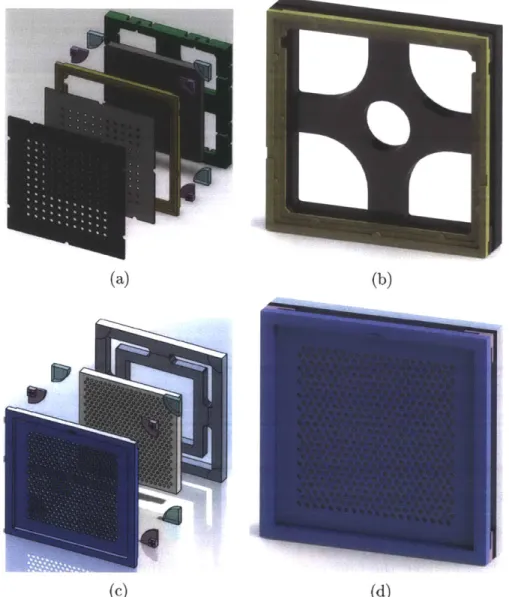
These concepts led to the initial iEPS 2.0 design, and experience with the 2.0 design shaped the changes which led to the first flight design, iEPS 2.2F. These two package designs are shown in Figure 2-3 as exploded and collapsed views. The package comprises four layers as depicted in Figure 2-4, the bottom three of which are permanently bonded together into a frame. Each layer has material and geometric features important to the overall device's functionality. The rationale for the features of each layer follows.
(a) (b)
(c) (d)
Figure 2-3: Exploded and collapsed views of the (a,b) iEPS 2.0 and (c,d) iEPS 2.2F designs as modeled with CAD 3oftware.
Package component nomenclature
Grid Frame
Alignment Layerm
Insulating Layer
Base Layer
Figure 2-4: A cross-3ection view of iEPS 2.0 with layer nomenclature. In the case of the uppermost layer, the unibody design is simply referred to as an extractor.
2.2.2
Base Layer Design
The base layer, or layer one, serves four main purposes in iEPS 2.x: (1) serving as the main structural component of the device, (2) providing a mounting location for the emitter substrate, (3) acting as the first line of defense against accumulation of propellant and formation of current leaks, and (4) providing an interface for mounting to test setups and eventually, propellant reserves.
Backbone of the Package Frame
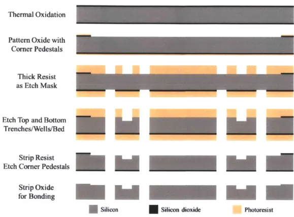
A striking difference between the previous design and the design of the iEPS 2.x package is the shift toward a very open structure. With this change, the rigidity and strength of the box-like, uni-body 1.0 frame was lost. To compensate for this change and to allow for the liquid trap features described in the subsequent section, the base layer was chosen to be thick, nominally 1 mm. This thickness was maintained throughout the design iterations, despite the eventual elimination of the liquid traps. Corners in the etched geometry were rounded to avoid stress concentration when under load as silicon is a brittle material and will easily cleave along crystal planes when mildly stressed.
In order to achieve the four-corner pillar design, the face of the base layer was recessed 25 to 3D pm everywhere except for at rounded areas at the corners as depicted in Figure 2-5. These pedestal- provided the bonding surface for the second layer and held the glass away from the interior where bonding was not intended.
Figure 2-5: An isolated view of a frame base layer corner where a pedestal is defined to prevent bonding anywhere but at the corners.
Fixture for the Emitter Substrate
An essential purpose of the frame, the base layer provided a surface onto which the emitter substrate could be affixed. The emitter substrate was adhered with an epoxy applied directly to the bare silicon surface. This was done manually with no coarse alignment assistance for the placement of the substrate chip. After some experiences with emitter chips debonding and worries about liquid transfer from substrate to frame, two design variations were introduced with iEPS 2.2, each of which addressed an individual problem. The first added small recesses to the central area of the base layer which were meant to act as epoxy wells for better adhesion to the structure. In the second, the entire substrate interface bed was recessed in order to introduce areas for epoxy at the chip edge where the interior bridged to the exterior of the frame. Placing epoxy there was meant to block liquid from wetting the silicon surface of the frame. The bed could also potentially act as a rough alignment feature for the emitter chip. Eventually, only the recessed bed variation was included in the iEPS 2.2F design, not as a way of preventing liquid transfer, rather as an optional feature to accommodate off-nominal emitter chip thicknesses (those in excess of 1 mm). Examples of the epoxy wells and chip bed variations may be found in Figure 2-6
(a) (b)
Figure 2-6: Examples of (a) the epoxy wells in iEPS 2.2 to improve emitter chip bonding and (b) the chip bed recess to improve bonding, block liquid movement, and accommodate over-tall chips.
First Defense Against Current Leaks
The most crippling failure of the original iEPS design was the development of current leaks within seconds or minutes of initial operation due to the transport of excess liquid propellant. To avoid this issue in iEPS 2.x, an open architecture was adopted. This move to an open design necessitated an increase in the footprint of the frame to 13 mm x 13 mm in order to maintain compatibility with the heritage emitter chip size.
The emitter chip was separated from the extractor supports by a gap, and the liquid would have to travel from the center of the chip edge along one of the frame arms to reach one. This was a change from about a 1-mm path along the electric field to 7 or more mm, mostly transverse to the field's pull. The liquid path is illustrated in Figure 2-7. Additionally, features were added to the design which further impeded the transport of liquid and the formation of a continuous liquid path, some of which were in the base layer. These features appear in the 2.0 and 2.1 designs as nominally 750-um deep trenches in the outer structure of the base layer. The trenches were intended to act as traps for the conductive propellant which would be unlikely to move down into them, against the attraction of the electric field. Initially, two design variations were made: one with five trenches etched into the upper and lower face of each corner support arm and the other with three above and two below. With the changeover to the 2.1 design, the number of trenches was changed to two above and one below in one design and none in the other. The reduction was an attempt to recover structural integrity. Eventually, it was determined that the trenches were unnecessary for liquid trapping with the open architecture and were done away with for the 2.2 design.
Interface to Test and Propellant Supply Equipment
Lastly, the base layer was also used as the interface between the thruster and op-erational support hardware. The underside of the thruster was kept flat for stable placement on surfaces. In the center, a porthole was included to allow for wetting
Base layer
side view
Liquid
path
Base layer
ton viewFigure 2-7: An illustration of a path that propellant would need to traverse in order to reach the corner posts and climb to the extractor electrode.
from the backside of the emitter chip and for connection of a propellant reservoir. [n the iEPS 2.0 and 2.1 designs, the circular porthole was maintained at the her-itage diameter of 3 mm. After testing showed that hydraulic impedance could reduce performance, the port was increased in area for version 2.2 as seen in Figure 2-8. Both square and circular ports were designed, the circular with a 6-mm diameter and the square with a 7-mm width. These amounted to approximately four- and seven-fold area increase, respectively. The square variant was chosen for the iEPS 2.2F configuration.
Figure 2-8: The four variation3 of the base layer in iEPS 2.2 showing the two port variants and the variation between epoxy wells and recessed chip bed.
2.2.3
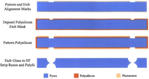
Insulating Layer Design
As mentioned, a major requirement for the package is the electrical isolation of the high voltage electrodes. In Courtney's original design, this was achieved through the combination of an oxide layer grown on the the silicon frame and the epoxy separating the extractor from the frame. In iEPS 2.2, the isolation is provided by a 500-pm thick glass layer of Corning Pyrex 7740. This layer is anodically bonded to both the base and alignment layers above and below it. Anodic bonding results in a siloxane layer forming between the Pyrex and bare silicon on each face. The combination of these siloxane layers and the thick glass lead to an insulating layer capable of resisting approximately 125 to 460 kV between the electrodes [9]. As the thruster is intended to operate two orders of magnitude below that, it is likely that only a defect in materials could precipitate a short through the frame. Surface contamination, however, is not precluded, but that is the reason for the open design of the thruster frame.
By virtue of the process used to shape the insulating layer, the walls interior to the frame come to a sharp inward-facing horizontal edge. This surface geometry further acts to prevent formation of liquid pathways as any liquid which reaches the apex will (1) be unlikely to traverse it due to surface tension and (2) may electrospray onto the grid or emitter substrate rather than reach the extractor.
2.2.4
Alignment Layer Design
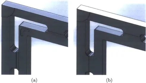
To avoid the difficulties of manual or jig-assisted alignment, a design was desired which made alignment of the emitter tips and the extractor apertures a feature of the component interface. As with Courtney's iEPS, the alignment of the emitter array to the frame is based on alignment marks etched into the frame. These appear on the upper face of each corner post as a crosshair as shown in Figure 2-9. The crosshairs are aligned at a wafer level to the shape of the corner posts. The corner posts act as a keyed interface to corresponding recesses in the underside of the extractor frame. Tolerances between the post walls and the extractor frame define part of the alignment
3cheme a3 is described in Section 2.2.6.
Figure 2-9: Each corner post of the frame is topped with an alignment crosshair for reference in machining the emitter array.
2.2.5
Extractor Layer Design
Two main extractor types were designed and manufactured: the grid frame with metal extractor grid and the unibody silicon extractor. While the grid frame was originally preferred for its thin, rigid, sputter-resistant tungsten grid and support for a downstream grid, the latter design was adopted for iEPS 2.2F due to the reliability of yield and geometry and due to the compatibility with batch production.
Grid Frame and Metal Extractors
The original extractor de-ign was made of two components: a silicon grid frame and the metal aperture grid(s) which it held. Solid silicon was used to form the grid frame. Rigid tungsten foil was used for the extractor and accelerator grids, as it could be made thin without risking 3ignificant deflection under electrostatic loading.
The grid frame is a 3quare -tructure which is designed to support the metal grids at their edges and i3 3hown in Figure 2-10. Recesses for interfacing with the package frame are at the cornerR of the underside of the grid frame. The upper side features two levels at which gridR can be fit. The deeper level is for the necessary extractor. The upper level can be fit with a secondary grid to modify the velocity of the extracted
Figure 2-10: To support the use of metal extractor grids, a silicon grid frame was designed to fit and align to the thruster frame. It contains a secondary level for the attachment of a downstream accelerator grid.
propellant. The depths of these levels is determined by the desired extractor-to-accelerator grid Rpacing. Additional recesses were added to the underside and top level to accomodate electrode leads.
Alignment keys are designed into both levels of the extractor for positioning of the metal extractor grids. These relied on tight tolerances between circular shapes. The key pattern for the extractors and accelerators were different so that there was no confusion regarding which similarly-sized piece fit where.
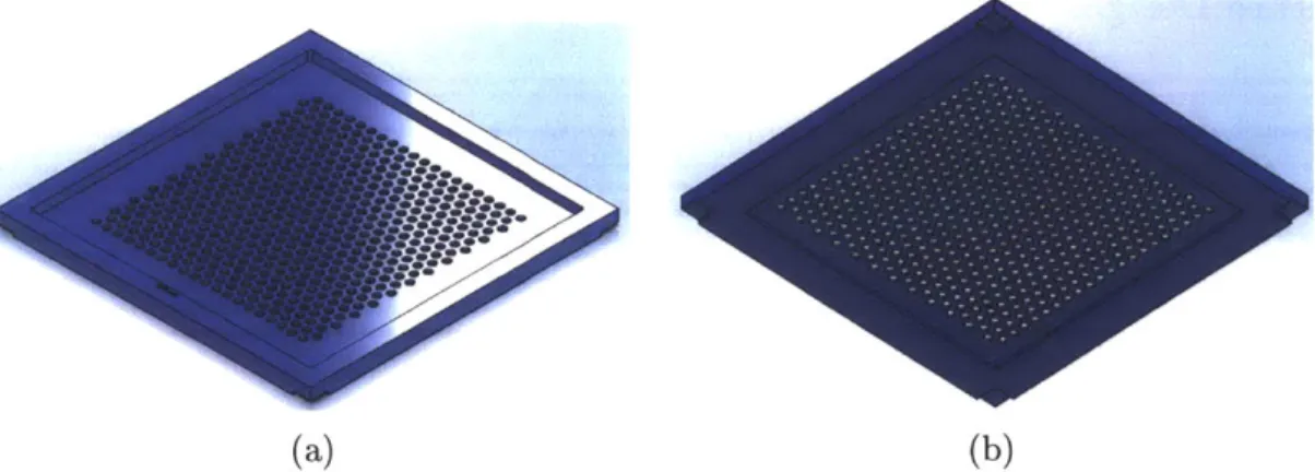
Unibody Silicon Extractor
Due to poor controllablity of the metal etching and the serial manufacturing process involved, a move to a 3ilicon-based component design was made. The silicon extractor wa- designed to be a 3ingle component. The underside of the silicon extractor is identical to the grid frame described above, however the upper side is simply a single well, at the bottom of which are the extraction apertures in a silicon sheet. Figure 2-11 -hows both sides of the unibody extractor.
A silicon-on-insulator wafer was used to precisely define a flat plane for the un-derside of the extractor which i3 level with the tops of the frame corner posts. This is achieved by the alignment recess features and central hole on the underside only etching to the depth of a uniformly-buried silicon oxide layer. The thickness of the 3ilicon aperture grid was initially intended to be nominally 100 to 150 pm, however
(a) (b)
Figure 2-11: The unibody silicon grid uses an SOI wafer to achieve a uniform under-side and DRIE etching to achieve deep, vertical under-sidewalls. Alignment of the apertures to the corner recesses is performed precisely at the wafer level.
in an attempt to reduce beam impingement, this was later reduced to a desired 20 to 30 pm. Control of this thickness in processing was found to be difficult, so the end thickness varies among production runs, dies on the wafer, and even across an individual extractor.
A metal coating was added to the design of the extractor for three reasons. The first was to allow for easy soldering to the component. Second was to improve charge relaxation in the grid so that any beam impingement charge can be redistributed quickly to maintain an even extractor potential. The final reason was to protect the underlying silicon from atmospheric oxygen and moisture so that it does not oxidize. Operational erosion of the metal layer will occur in a near-vacuum where the reduced presence of oxygen will oxidize the silicon much more slowly.
Variations in the design included three aperture diameters and various solder well shapes. Aperture diameters tested were 250, 275, and 300 Am, and the largest was chosen for the iEPS 2.2F configuration. Solder well variations tested included 200, 300, and 400 pm circles and rounded slots, and long U-shaped raceways of the same widths. Both through holes and pots were tested. It was determined that the simple rounded slot wells worked, and that the variation in diameter was not critical; so they were chosen in the interest of structural integrity and manufacturing ease.
Future Designs
Several design variations of the unibody silicon extractor were considered, but not fabricated. The two main drivers were reduction of beam current and an interest in adding an acceleration grid.
Any propellant which impinges upon the extractor electrode directly reduces the performance of the device in terms of thrust, efficiency, and lifetime. Two-dimensional electrostatic modeling of the effect of dimensional variation between the aperture and emitter was done to inform considerations of increasing aperture diameter and reducing grid thickness. An example field solution and the field dependence with geometry are presented in Figure 2-12.
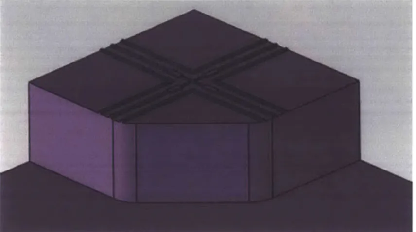
It was found that the shape of the extractor electrode downstream of the extractor opening has little effect on the tip electric field intensity. Over the range in which aperture variations have been produced, the aperture diameter changes the electric field intensity at the emitter tip by t5 to 10%. These two results lead to the conclusion that large, diverging apertures in a thick grid can achieve similar emission conditions as slightly smaller cylindrical apertures, while potentially reducing beam impingement and without losing rigidity. Thus, a new extractor design utilizing isotropic etching was conceived and is conceptually illustrated in Figure 2-13. An added benefit of such a design is the potential for an improved depth uniformity across the wafer with the use of a different etch technique. The downside, though, is that the mask geometry will depend on the substrate thickness.
A downstream grid adds the capability of operating in multiple specific impulse and thrust regimes with a single system when power-limited. This capability has the potential to allow the use of a single propulsion system for drastically different maneuvers. Coffman showed the relationship between flight time and change in I , and the effects of efficiency on this reduction 10]. By reducing the specific impulse at fixed power, the thrust can be increased to directly reduce the mission time. Inversely, the specific impulse can be increased in order to reduce propellant consumption across the same impulse change. With these multi-modal benefits in mind, a conceptual
Tip Apex Normal Electric Field as a Function of Extractor Geometry Potential for 50-um Thick Grid, 300-um Aperture, 0 Grid-Tip Separation
x1O5 A 1000 20 1000 is 900 10 W 700 0 a 600 500 -5 400 -10 300 -15 200 100 -20 -20 -10 0 10 x10- 10 x-dirnension Wm V 0 0 35- 30-25 20 15 10
- Varying Grid Thickness
5 - Varying Aperture Diameter
- Varying Grid-tip Separation 0
0
G 0 1T5 2k0 r 2Arr5 3Dr 0 nX 10dp
Grid Thickness, Aperture Diameter, Grid-tip Separation (in)
(a) (b)
Figure 2-12: A two-dimen-ional electrostatic model was made in COMSOL Multi-physics to better understand the influence of emitter geometry and position on the tip electric field intensity. An example field solution is presented in (a) and the geo-metric dependencies in (b). Note that there is an insensitivity to grid-tip separation and downstream 3hape in the range shown, but that aperture diameter is sensitive to small openings. Aperture diameters of interest range from 200 to 400 pm.
Current Design
Impingement
Modified
Equal Aperture Size Isometric Etch Profile
Figure 2-13: A divergent aperture is conceptually shown to reduce the amount of beam impingement on the extractor despite the increased thickness of the grid.
design for a dual-grid, unibody extractor component was devised.
Achieving multiple grid layers in a solid component will require the bonding of multiple thin wafer-. The extractor is constructed as described in the previous section; however the thickness of the upper portion will need to be reduced in consideration of the inter-electrode gap desired and any separation layers that need to be accommo-dated. A second wafer would be patterned with the accelerator apertures and then bonded to the extractor layer. Another option is to replace the second wafer with a thin film metal on an insulator as the downstream grid.
elec-insulator
A
A
AcceleratorIAAAAAAAr
* Silicon
* Silicon dioxide Designs for decreasing
G inter-electrode gap
Figure 2-14: Depending on the desired electrode spacing in a unibody dual-grid extractor-accelerator component, there are multiple design options including oxide-insulated, oxide-insulated with offset, glass-oxide-insulated, metalized glass, or more.
trodes while also maintaining a small inter-electrode distance. This can be achieved by bonding wafers with oxidized surfaces such that there is an insulating plane be-tween them. Alternatively, a thin layer of glass could be used as a separator similar to its use in the thruster frames. The choice between these options will be based on the optimal inter-electrode gap and the availability of thin glass substrates. A cross-section for each concept iR shown in Figure 2-14.
2.2.6
Component Alignment Schemes
For efficient operation, it is desirable for the emitter tips to be coaxial with the extrac-tor apertures. Misalignment can cause asymmetric electric fields, off-axis propellant acceleration, and increased beam impingement. As the tips are on the order 10 Am in diameter and the apertures have been sized between 250 and 300 Am, a maximum misalignment in the 10 to 20 pm range has been deemed acceptable. The alignment 3cheme developed for iEPS 2.x utilizes low-tolerance interfaces during assembly to ori-ent precisely aligned, manufactured features to one another. In short, crosshairs on
the alignment layer dictate the position of the emitter tips, and the interface between the frame corner posts and the extractor recesses defines the position of the apertures. In the case of the grid frame, alignment of the metal extractors implemented another low-tolerance interface. Alignment inaccuracy during manufacturing of the alignment features determines the minimum achievable misalignment in practice.
Of the four frame-extractor interfaces, two opposing corners have a 50-pm toler-ance, one has a 20-/,m tolertoler-ance, and the final corner has a -2-um tolerance. This final corner has an expected zero-tolerance once undercutting during etching is ac-counted for. The larger tolerances provide for ease of assembly, but by pushing the extractor into one corner, the alignment error can be driven, in principle, to zero. The alignment interfaces are shown with their tolerances in Figure 2-15. In practice, there will be an imperfection, however with the constraints of the design, the misalignment is limited. For a bi-directional linear displacement, the maximum misalignment is v/202
+
202 /im = 28.3 pm. A rotational misalignment introduces more complicated geometry, however the maximum center-to-center misalignment of a single aperture with respect to the frame is less than 50 pm, and the average across all apertures is below 36 ftm. In practice, these values do not hold due to inaccuracies inherent to the frame, extractor, and emitter manufacturing techniques which misalign the alignment features with respect to one another.Alignment of the etched features in the two components is a result of wafer-level alignment on an optical stage during photolithograpy. This introduces misalignment which varies in magnitude across the wafer. While the misalignment can be less than ten micrometers at the alignment marks themselves, in general it increases radially, so the central dies will be best aligned, and the edge dies will the most misaligned. Photolithography misalignment will be largest between the aperture positions and the extractor alignment recesses as these are aligned on opposite sides of the wafer using virtual positions in an alignment tool.
Due to difficulties in controlling the exact geometry of the metal etching, the alignment between the grid frame and the metal grids was unpredictable as it involved trial and error in choosing the design of the extractor photolithography mask. This
wa3 a main reason for developing the unibody extractor.
50 gm
+
0--gap
gap,
50 pm
gap
Figure 2-15: The four corner posts slot into recesses on the extractor underside. This allows for alignment of the apertures to the frame. Because the emitter tips are also frame-aligned, this should result in a low misalignment of tips to apertures.
Updates to the alignment Rcheme will likely include tighter tolerances and modified emitter alignment marks. Tighter tolerances are desired as it has been determined through experience that ease of assembly will not suffer from less "wiggle" room, and that the best alignment is actually achieved through additional adjustments with a microscope. Modifications to the alignment marks will make spotting them in the microscope used for emitter manufacturing easier, and they will reduce the occasional confusion with the wafer-level alignment marks.
2 pm
Chapter 3
Manufacturing the Thruster Package
All components of the iEPS 2.x thruster package were manufactured in the MIT Microsystems Technology Laboratory using well-understood microelectromechanical systems (MEMS) and integrated circuit (IC) industry tools and processes. These processes ranged from the complicated chemistry of high temperature reacting gas film growth and deposition to simple manual application of masking materials. Each device layer was processed separately before being assembled into the package. The three layers of the thruster frame were permanently bonded at the wafer level, while the extractor layer was attached once emitter manufacturing and assembly were com-pleted.
In part, this chapter summarizes the manufacturing processes at various device levels including the challenges encountered in developing and executing a successful process. Additional detail is provided for the processes in Appendix A. First, though, a short introduction to the types of processes used is given.
3.1
Microfabrication Basics
In order to inform the discussion of component manufacturing, a summary of the basic processes employed is provided with reference to their general applicability to this work. Where prudent, additional process detail is provided where context dictates.
3.1.1
Raw Materials
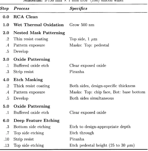
In the manufacturing of MEMS and IC devices, the standard form of raw material is the wafer. These are most commonly composed of single-crystal silicon formed into a thin disk, though also common are quartz, glass, and gallium arsenide. Ad-ditionally, bonded silicon wafers with an intermediate silicon oxide layer, known as silicon-on-insulator (SOI) wafers, can be sourced pre-made. Dopants can be used in the semiconductors to precisely control the bulk conductivity. These wafers come in standard sizes. The purity, doping, conductivity, and dimensional statistics are tracked by the manufacturer and tightly controlled. The work discussed here used silicon, Corning Pyrex 7740, and SOI wafers exclusively in the 150-mm (6 in.) diam-eter standard.
3.1.2
Thin Film Growth and Deposition
While the base material comprises the final structure, it is often necessary to modify the surface in order to define features, protect the pristine condition of the surface, or alter the surface properties for functionality. This can be achieved by initiating a chemical reaction at the surface or by mechanical or chemical deposition of material. All three types were employed for all three aforementioned reasons.
Thermal Oxide Growth
Pure silicon naturally reacts with oxygen to produce silicon dioxide. When the bare silicon of a wafer is exposed to the air, a thin (on the order of tens of angstrdms) native oxide layer will form. At high temperatures (800 to 1200 0C), at high oxygen
concentrations, and in the presence of water vapor, this process accelerates, though the thickness growth rate slows as it is is diffusion-limited. Furnaces have been developed to provide these conditions and are regularly used to grow oxide on silicon in the range of a few hundred nanometers to two micrometers at the extreme. This process will consume some of the surface silicon, and if the oxide is removed, the wafer loses some thickness. Thermal oxide growth was primarily used in this project
for protection of pristine silicon bonding surfaces and as an etch mask for shallow etches.
Polycrystalline Silicon Deposition
By pyrolysis, an amorphous polysilicon layer can be deposited on a substrate. This process occurs at high temperature (575 to 650 'C) such that silane (SiH4)
sponta-neously decomposes into silicon and hydrogen. The deposition rate is on the order of 10 nm/min and depends on the temperature and on the silane concentration which can be controlled directly or also through control of a non-reacting nitrogen background flow. For this work, Polysilicon is deposited as an etch mask against hydrofluoric acid for the Pyrex insulating layer.
Chemical Vapor Deposition
In chemical vapor deposition (CVD), volatiles or a mix of reacting gases are intro-duced to the surface of a wafer and the products are deposited. This is usually done at low pressure (milli- or microTorr) and enhanced by energizing the gases into the plasma state. CVD can deposit various films on a substrate based on the chemicals in-troduced, however the thickness is limited by the stresses introduced in the formation of the film which, if too high, can delaminate the film. For the work herein,
plasma-enchanced CVD (PECVD) was employed to deposit a thick silicon dioxide layer on the extractor substrate to be used as a hard mask resistant to plasma etching.
Electron Beam Physical Vapor Deposition
Electron beam (e-beam) evaporation employs a hot filament and accelerating elec-trode to bombard a target with electrons, thereby heating it to its melting point. Some of the melted target material then vaporizes under vacuum and condenses on any cold (below melting) surfaces it encounters. If a substrate is placed in the cham-ber with the vapor, it will be coated by the heated material. Rotating and moving the substrate can ensure even film deposition. The thickness of the layers deposited are limited by film stresses. Additionally, due to material incompatibilities, it may be
necessary for a final surface film to be preceded by an adhesion layer film. E-beam evaporation was used to deposit metal on the unibody silicon extractors as a way of preventing oxidation, improving surface charge relaxation, and enabling soldering.
3.1.3
Contact Photolithography
Contact Photolithography is a method for precisely defining two-dimensional pat-terns in a light-reactive surface film. This film can then be used as a protective mask for defining patterns in underlying films, for selectively removing substrate material by etching, or for selectively preventing deposition of other materials. Generally, the pattern is initially produced on a metal-coated glass plate using laser writing or on transparent plastic film by printing. These masks can then be used to protect a spun-on liquid or laminated film polymer from ultraviolet light. Hexamethyldisilazane (HMDS) is often deposited on the substrate prior to coating with liquid photopolymer to promote adhesion. The polymer will react when dosed with the light and either become more soluble (positive) or less soluble (negative) in a developing solution. The polymer is then selectively dissolved, exposing the underlying material. Exposed material can be acted upon by plasma, acids, or physical deposition processes. Ex-posure of the pattern can be precisely aligned (usually within 10 micrometers of two points) to existing features on the wafer using an x-y stage and microscopes. In the case of the work described here, photolithography of positive spin-on photopolymer was extensively used to protect surfaces from wet and dry etches. In total, ten pat-terns, not including version variations, are used for to form any one iEPS 2.x package configuration.
3.1.4
Wet Etching and Cleaning
Wet etching and wet cleaning are the submersion in an acid, base, or reactive bath in order to remove material. The benefits of wet processing are its low-tech requirements and amenability to batch processing. However, fluid dynamics and local reaction product buildup can lead to variation of etch rates across samples in the same bath.
Moreover, delicate devices often have difficulties surviving the mechanical forces of the bath and subsequent drying processes. Also, insufficient drying can ruin small components. While there are myriad uses for wet processing, in this work it was mainly used to strip organic materials, to pattern or remove oxide and silicon films, and to etch glass. The common "piranha" solution used to remove organics and metals consists of a 1:3 mixture of hydrogren peroxide and sulfuric acid.
3.1.5
Deep Reactive Ion Etching
Deep Reactive Ion Etching (DRIE) is a variation on RIE which uses alternating poly-mer deposition and directed plasma etching to achieve high-aspect-ratio anisotropic removal of substrate material. It is also commonly known as the Bosch Process. The etch step employs sulfur hexafluoride plasma which eschews fluorine radicals that react with the silicon. The etch rate drops with the depth of the target surface (dif-fusion limitation) and the exposed area (reaction loading). This technique is used to form the features seen in the silicon components of this work ranging from a few micrometers deep to through etches of the millimeter-thick base layer.
3.1.6
Anodic Bonding
When multiple wafers need to be semi-permanently or permanently fused, there are several bonding techniques to choose from. In this work, anodic bonding was used to permanently fuse the three layers of the thruster frame. In anodic bonding, two substrates are held between opposite polarity electrodes, inducing an electric field within the material. Depending on the material composition, charge carriers will flow to one or both surfaces. With the correct setup, depletion or concentration of charge can occur at the substrate interface and precipitate a chemical reaction between the surfaces resulting in the formation of a continuous material. In this work, anodic bonding between bare silicon and Pyrex was performed twice per frame stack. At high temperature (250-400 'C), transport of sodium ions away from the contact area results in a negative volume charge near the interface. A corresponding positive