Commercialization of Bit-Patterned Media
by Ria Esterina S.Si. Physics
Universitas Pelita Harapan, 2007
SUBMITTED TO THE DEPARTMENT OF MATERIALS SCIENCE
AND ENGINEERING IN PARTIAL FULFILLMENT OF THE REQUIREMENTS FOR THE DEGREE OF
MASTER OF ENGINEERING IN MATERIALS SCIENCE AND ENGINEERING
AT THE
MASSACHUSETTS INSTITUTE OF TECHNOLOGY SEPTEMBER 2009
©2009 Massachusetts Institute of Technology. All rights reserved.
Signature of Author: ______________________________________________________ Department of Materials Science and Engineering
August 14th, 2009
Certified by: _____________________________________________________________ Caroline A. Ross Toyota Professor of Materials Science and Engineering Thesis Supervisor
Certified by: _____________________________________________________________ Adekunle O. Adeyeye Associate Professor of Electrical and Computer Engineering, NUS, Singapore
Thesis Supervisor
Accepted by: ____________________________________________________________ Christine Ortiz Associate Professor of Materials Science and Engineering
3
COMMERCIALIZATION OF BIT-PATTERNED MEDIA
by Ria Esterina
Submitted to the Department of Materials Science and Engineering on August 14th, 2009 in partial fulfillment of the requirements for the Degree of
Master of Engineering in Materials Science and Engineering
ABSTRACT
Realm of data storage density has expanded from gigabyte- to terabyte-domain. In such a high areal density, bit-patterned media is a promising candidate to overcome the superparamagnetic limit faced by the conventional continuous media. However, the patterned media concept has not been realized in mass production due to several reasons. Beside the stringent requirement of high-resolution lithography, high production cost is inevitably the major challenging problem. If a low-cost mass fabrication scheme is available, bit-patterned media will be an innovative way in hard disk technology to achieve a storage density beyond 1 Tb/in2.
The objective of this thesis is to review the patterned media technology and discuss its challenges and commercialization viability. A possible mass-production scheme is discussed. Electron beam lithography and self assembly process of block copolymer are used to fabricate the master template. To ensure high throughput, template replication as well as disk fabrication are carried out by UV-nanoimprint lithography (UV-NIL).
Considering the large opportunity of patterned media to enter the market, a business plan was constructed. Enormous profit was proved to be possible when the barrier of technology, intellectual property, and funding can be surpassed. Therefore, patterned media shows to be superior in terms of performance and cost compared to the conventional media.
Thesis supervisor: Caroline A. Ross
Title: Toyota Professor of Materials Science and Engineering Thesis Supervisor: Adekunle O. Adeyeye
4
Acknowledgements
There are a lot of people who have made it possible for me to complete this thesis. First, I would like to thank Prof. Caroline A. Ross for her guidance and advice. Thank you for making this project to be a pleasurable learning experience. I am also deeply indebted to Prof. Adekunle Adeyeye from NUS, Singapore, who has always been encouraging. His advice and critiques have shaped the direction and vision of my thesis. I have also received helpful comments from Prof. Eugene Fitzgerald and Dr. Andreas Wankerl for the technology evaluation aspects.
Next, I would like to express my appreciation to Yudi for helpful discussion in developing the business plan. Thanks also to Iongying for introducing me with Zotero software and to Rhea for helping me print the draft.
Lastly, for my parents and sister in Bali, thank you for your love, support, and faith in me. Without their support, I would never have achieved what I intended to in life.
5
Table of Contents
Abstract ... 3 Acknowledgements ... 4 Table of Contents ... 5 List of Figures ... 7 List of Tables ... 10 Chapter 1 Introduction ... 11Chapter 2 Bit-Patterned Media Technology ... 13
2.1. Fundamentals of Magnetic Recordings ... 13
2.2. Limitations of Conventional Perpendicular Media ... 15
2.3. Prospects of Bit-Patterned Media ... 17
2.4. Challenges to Bit-Patterned Media Technology ... 18
2.4.1. Media Fabrication ... 18
2.4.2. Magnetic Properties Uniformity ... 20
Chapter 3 Fabrication of Bit-Patterned Media ...27
3.1. Structures of Recording Media ... 27
3.2. Template Fabrication ... 29
3.3. Media Fabrication ... 35
Chapter 4 Market Opportunity ... 40
4.1 Technology Supply Chain ... 40
4.2 Competing Technologies ... 41
4.2.1. Heat-Assisted Magnetic Recording ... 41
4.2.2 Microwave-Assisted Magnetic Recording ... 43
4.2.3. Exchange Coupled Composite Media ... 45
4.2.4. Comparison among HAMR, MAMR, and ECC media ... 46
4.2.5. Outer Competitor ... 47
4.3. Complementary Technologies ... 48
4.3.1 Head Technology ... 48
4.3.2. Disk Drive Electronics ... 53
6
4.5. Target World Market ... 57
Chapter 5 Business Plan ... 60
5.1 Operational Plan ... 60
5.2 Capitalization ... 63
5.3 Financial Plan ... 64
Chapter 6 Conclusion ... 73
References... 75
Appendix 1: Block Copolymers on Chemically Heterogeneous Striped Surface .... 80
Appendix 2: NIL Cost Calculation ... 83
Appendix 3: Ion Miller Throughput Calculation ... 84
Appendix 4: Sputtering and Dry Etching Machine Throughput Calculation ... 85
7
List of Figures
Fig. 1.1. Areal density trend ... 11
Fig. 2.1. Hysteresis loop of a permanent magnet ... 13
Fig. 2.2. Magnetostatic and domain-wall energies versus particle size ... 14
Fig 2.3. Magnetization change of a very small particle (single-domain particle) ... 14
Fig 2.4. Hysteresis behavior of a single-domain particle with the external field applied along (a) the easy axis, and (b) the hard axis ... 15
Fig 2.5. Hysteresis behavior of superparamagnetic materials ... 16
Fig 2.6. Coercivity versus size for a small particle ... 16
Fig. 2.7. Disk coercivity versus areal density evolution ... 17
Fig. 2.8. Schematic of (a) conventional thin film medium, consisting of single-domain grains. Bits are represented as transitions between regions of opposite net magnetization. Each bit occupies an area of tens to hundreds of grains. (b) Patterned medium with in-plane magnetization. Now the bits are defined lithographically with a period p. The bits can either be polycrystalline (indicated by dotted lines) or single crystal, but they magnetically act as single domains. (c) Patterned medium with out-of-plane magnetization. The period, height, and diameter are p, h, and d, respectively. Binary one and zero are indicated ... 18
Fig. 2.9. Coercivity distribution map of patterned media obtained by dot-by-dot analysis. The contrast indicates Hc ... 21
Fig. 2.10. MFM image of patterned media written by ring head. Black lines indicate a trajectory of the ring head ... 21
Fig. 3.1. Proposed fabrication plan of BPM ... 27
Fig. 3.2. Functional layers of perpendicular recording medium. Layers are not to scale ... 28
Fig. 3.3. Chemically-assisted pattern generation ... 30
Fig. 3.4. SEM images of lamellae-forming PS-b-PMMA block copolymer films (L0 = 48 nm) on chemically nanopatterned substrates as a function of LS (LS = 42.5 nm, 47.5 nm, and 52.5 nm) and composition of the random-copolymer brush used to create the chemical pattern. The blue beads represent PS units and red beads represent PMMA units in the random block copolymer brush layer. Higher percentages of PS in the random block copolymer brush produce the higher chemical contrast of the surface patterns to PS-b-PMMA. Stronger chemical contrast favors replication of the underlying pattern ... 31 Fig. 3.5. Process to create lithographically defined, chemically pre-patterned surfaces, and subsequent directed assembly. (A) Electron-beam lithography patterns at LS = L0 (left) and LS = 2L0 (right). (B) Chemical contrast on the substrate after O2 plasma
8
exposure on the e-beam–defined spots above. (C) Block copolymer thin film. (D) Guided self-assembly in registration with the underlying chemical pattern
... 32
Fig. 3.6. Rotary-stage EBL ... 32
Fig. 3.7. Servo pattern element write using the CSFL function. (a) Groove and dot, (b) dot and shifted elliptical dot, (c) groove and right-angled groove, and (d) different-length pits with various doses ... 33
Fig. 3.8. Self-assembly of block-copolymer ... 35
Fig. 3.9. UV-NIL process for patterned media ... 36
Fig. 3.10. Patterned media imprint examples ... 36
Fig. 3.11. Steps in the fabrication of patterned magnetic media ... 37
Fig. 3.12. Magnetic spacing requirements for HDD ... 38
Fig. 3.13. Illustration of high throughput disk fabrication with the proposed fabrication plan ... 39
Fig. 4.1. HDD supply chain ... 40
Fig. 4.2. Globalization of HDD supply chain ... 41
Fig.4.3. Diagram of HAMR writing process ... 42
Fig. 4.4. MAMR process ... 43
Fig. 4.5. (a) Schematic illustration of the ac field assisted perpendicular head design. (b) Illustration of magnetization precession of the field generating layer facilitated by the spin torque. int is the interlayer exchange coupling surface energy density, MS is the saturation magnetization, and is the thickness ... 44
Fig. 4.6. Illustration of a grain in an ECC medium. It consists of a magnetically hard part and a magnetically soft part ... 45
Fig. 4.7. Basic structure of proposed ECC media ... 46
Fig. 4.8. Comparison between HDD and SSD ... 47
Fig. 4.9. (a) Evolution of head technology; (b) Structure of CPP TMR and CPP GMR heads ... 49
Fig.4.10. Trends of data transfer rate for high-end HDD systems and allowed resistance-area product (RA) of read head sensors with CPP structure versus resistance-areal density ... 50
Fig 4.11. Estimated required RA of CPP-GMR for higher recording densities for output signal voltage = 1.5 mV, head efficiency = 30%, sense current density = 100 MA/cm2, power consumption of sensor element = 0.6 mW ... 51
Fig. 4.12 Standard feedback block diagram ... 54
9
Fig. 4.14. HDD shipments and revenue ... 58
Fig. 4.15. HDD industry forecast and market share ... 58
Fig. 4.16. Worldwide PC shipments forecast ... 59
Fig. 5.1. Diagram plots of the price-per-GB for NAND Flash memory and HDDs. As of Mar 2009, NAND Flash memory is about US$1.25 per GB. Prices through Mar 2009 from Nihon Keizei Shimbun, beyond that forecasts by Nikkei Electronics ... 65
Fig. 5.2. Cost/GB for 1Tb/in2 as a function of production volume ... 67
Fig. 5.3. Cost/GB as a function of production volume and areal density ... 67
Fig. 5.4. Maximum cost per disk and cost per GB for different areal densities ... 69
Fig. 5.5. Contour representation of cost/GB as a function of production volume and areal density ... 69
Fig. 5.6. Annual profit projection of HDD media company with BPM technology ... 71
Fig. 5.7. Profit margin projection of HDD media company with BPM technology ... 72
Fig. A1.1. When the width of the stripes is much larger than the size of a block, the copolymers may either form 3D brushes within each stripe (a) or 2D brushes along the interfaces between the stripes (b) ... 80
Fig. A2.1. Imprio® HD2200 ... 83
Fig. A3.1. FAB104 ion miller system ... 84
Fig. A4.1. PT770 Dry Etcher system ... 85
10
List of Tables
Table 2.1. Examples of required lithography dimensions for patterned media ... 19
Table 4.1. Read head challenges ... 48
Table 4.2. Geometrical requirements for head for patterned media ... 48
Table. 4.3. Various design scenarios for BPM recording systems ... 52
Table 4.4. Several relevant patents to BPM ... 55
Table 5.1. Comparison of start-up company formats ... 60
Table 5.2. Additional cost breakdown for PV = 100 M disks/year and Capacity = 600 GB/disk ... 62
Table 5.3. Start-up capital calculation for PV = 100M disks/year ... 63
11
1. Introduction
Hard Disk Drive (HDD) is a robust industry with shipments of 593.2 million units in 2008, up by 14.93 percent compared with 516.2 million units in 2007, according to a market research firm iSuppli Corp. [1]. The history of magnetic recording technology dates back to 1898 when Valdemar Poulsen patented the telegraphone [2]. Its application to HDD industry began in 1956 when IBM introduced Random Access Method of Accounting and Control (RAMAC) with an areal density of approximately 2 kb/in2 [3]. Since then, the areal density of HDD has been improved to meet the ever-increasing requirement of performance. As shown in Fig. 1.1, there has been more than a three-order-of-magnitude increase of areal density since 1990s, suggesting that HDD industry is on the way to enter the terabyte-era. To ensure a smooth transition, there is a strong driving force for HDD industry to shift from the conventional continuous-grain magnetic media to bit-patterned media (BPM).
Fig. 1.1. Areal density trend [4].
Conventional HDD records data by writing the magnetization pattern on a thin film with perpendicular magnetic anisotropy axis. However, terabyte storage density is not a possible scheme with this current conventional method. In continuous thin film media,
12
one bit consists of several grains or magnetic units. As the density of data storage increases, superparamagnetic phenomenon occurs. Magnetic recording trilemma, among SNR, areal density, and thermal stability, is inevitable. Consequently, perpendicular magnetic recording (PMR) technology is predicted to reach its limit at 600 Gb/in2 [5]. BPM, firstly proposed in 1989 by Nakatani et al. [6], is a promising candidate to surpass this limitation. BPM stores the data on a uniform array of magnetic cells, each of which will store one bit of information. In contrast with PMR, the bits in BPM, either polycrystalline or single crystal, act as single-domain magnets. The data density of BPM could extend to 1000 times that of continuous media[7].
Nonetheless, the commercialization of BPM is faced with several challenges. Despite the fact that patterned media concept has been reported since 20 years ago, it has not been realized in mass production. There had been various proposals of possible mass-production schemes until 2008 when two major data storage companies, Hitachi and Seagate, shared the same view on a single most optimum manufacturing strategy for BPM [8],[9]. Beside the stringent requirement of high-resolution lithography, high production cost is inevitably the major challenging problem. Not until its production cost is lower or comparable to the cost of conventional method will the commercialization of BPM be feasible.
The objective of this thesis is to review the BPM technology and discuss its commercialization viability. A brief introduction about HDD and its recording schemes is given in Chapter 1. The idea of BPM technology and its manufacturing method are detailed in Chapter 2 and 3. The market opportunity and business plan are discussed in Chapter 4 and 5, respectively. Finally, Chapter 6 concludes the thesis.
13
2. Bit-Patterned Media Technology
2.1. Fundamentals of Magnetic Recordings
HDD belongs to the group of magnetic storage. It integrates many key elements, one of which is the magnetic recording media. To have a clear picture of the magnetic recording media, it is essential to understand the physics behind the magnetic recording process.
Magnetic properties of a material are typically characterized by its hysteresis loop, as shown in Fig. 2.1.
Fig. 2.1. Hysteresis loop of a permanent magnet[10].
Hysteresis is the result of an irreversible conversion from energy to heat, with the energy lost in going round a cycle is equal to the area inside the major loop. In this loop, we can observe two important properties of a permanent magnet: remanence and coercivity. Remanence is the ability of a material to retain its magnetization after the magnetic field causing the material to achieve saturation is removed, while coercivity is the amount of required reverse magnetic field to bring the magnetization back to zero [11]. It is remanence which makes the recording process possible.
A particle can have either multi domains or single domain depending on its size. Different magnetic domains on a particle will be separated by a transition zone in between which is called the domain wall. A large particle will show multi-domain
14
behavior while a particle less than 1 µm long is single-domain in zero external field [11]. This phenomenon is derived from energy consideration. As can be seen in Fig. 2.2, The domain wall energy is proportional to the area of the wall (~L2) while the magnetostatic energy is proportional to the particle volume (~L3). Therefore, a large particle will arrange itself to minimize its magnetostatic energy by creating magnetic domains, and hence multi-domain configuration. Meanwhile, a smaller particle will prefer a single-domain configuration to minimize its single-domain wall energy.
Fig. 2.2. Magnetostatic and domain-wall energies versus particle size[11].
For a small single-domain particle under an applied magnetic field, the magnetization process proceeds by rotation of the total magnetic moment of the particle, as shown in Figure 2.3. The hysteresis behavior is depicted in Figure 2.4. Due to anisotropy, a particle will have easy and hard axes. If a sufficiently large magnetic field is applied parallel to the hard direction of the particle, the M-H curve will be linear, which means there is no hysteresis. The magnetic moment will rotate towards the field direction and rotate back to its easy axis when the field is removed. On the other hand, if the field is applied along the easy axis, the magnetic moment must rotate through the hard direction to fully reverse its orientation. In this regard, the coercivity will be large, and the particle will exhibit square hysteresis loop.
15
Fig 2.4. Hysteresis behavior of a single-domain particle with the external field applied along (a) the easy axis, and (b) the hard axis[13].
For magnetic recording application, it is preferable to use small single-domain particles with the writing magnetic field applied parallel to the easy axes. The recorded data is stable because a considerable force is required to switch the orientation of the magnetic moment.
2.2. Limitations of Conventional Perpendicular Media
In conventional perpendicular media recording (PMR), one bit consists of many grains. To achieve high areal density, the bit must be as small as possible. In this case, to ensure high signal-to-noise ratio (SNR), a large number of grains per bit cell is needed. Thus, the size of the grains must also be lowered. However, as the scaling down continues, the superparamagnetic effect is inevitable. Superparamagnetism is anhysteretic behavior of magnetization loop which is observed at temperature well above the blocking temperature (TB) [14]. Superparamagnetism is similar to paramagnetism, except that the magnetization is much larger in the former because each particle behaves like a giant spin, as depicted in Fig. 2.5.
In superparamagnetism, a particle exhibits zero coercivity and zero remanence. As we decrease the particle diameter, the coercivity will increase until the particle has reached a critical size, below which the coercivity will decrease down to zero (Fig. 2.6). This critical size depends on the particle anisotropy. Typically, for an anisotropic spherical particle at room temperature, superparamagnetism will be observed when the particle diameter is less than 100 Å [15].
16
Fig 2.5. Hysteresis behavior of superparamagnetic materials [16].
Fig 2.6. Coercivity versus size for a small particle [13].
Due to this paramagnetic effect, the small grains become magnetically unstable and tend to spontaneously flip, causing loss of data. To maintain magnetic stability for about 10 years, the ratio between magnetic energy and thermal energy of a magnetic medium should not be less than 40 (KV/kT 40, where K is the anisotropy constant, V is the grain volume, k is the Boltzmann constant, and T is the temperature in Kelvin) [17].To prevent data loss, we need to use a material with high anisotropy constant K. However, this material will then possess a very high coercivity and need a very high magnetic field to be magnetized for data recording. The coercivity evolution due to increase in areal density is shown in Fig. 2.7. The three requirements of high SNR, high areal density, and
17
good writability thus create a trilemma in magnetic recording. PMR scenario is thus expected to reach its limit at an areal density of 600 Gb/in2 [5].
Fig. 2.7. Disk coercivity versus areal density evolution [18].
2.3. Prospects of Bit-Patterned Media
In BPM technology, the trilemma in magnetic recording is addressed by modifying the recording media. The media are patterned so that one bit is one magnetic entity. The restriction KV > 40 kT still holds except that V is now the bit volume, which is obviously larger than the grain volume. Thus, the thermal limit can be satisfied without sacrificing the writability. Stable high-density media can be achieved by using this technology. Areal density beyond 1Tb/in2 is expected to be achievable in BPM. Currently, the best achievable resolution of block copolymers (BCP) is 3 nm, equivalent to approximately 10 Tb/in2 areal density [19].
Transition jitter is also eliminated in BPM since the bits are isolated one from another. Moreover, unlike the conventional media, the track width in BPM can be reduced without affecting the SNR. This can further increase the areal density of BPM [5]. To isolate the
18
magnetic entities, physical spacing or filling of non-magnetic materials can be used. The comparison between continuous media and BPM is shown in Fig. 2.8.
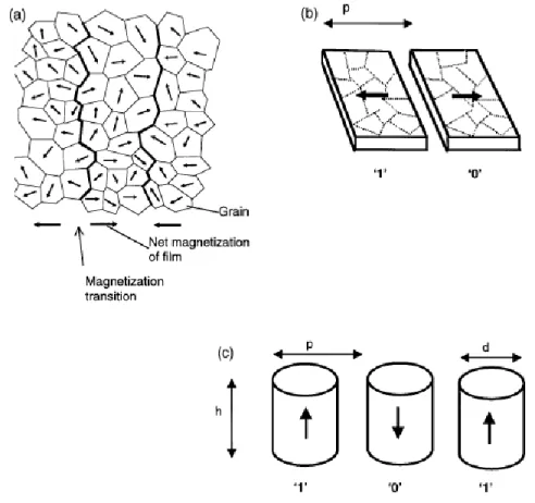
Fig. 2.8. Schematic of (a) conventional thin film medium, consisting of single-domain grains. Bits are represented as transitions between regions of opposite net magnetization. Each bit occupies an area of tens to hundreds of grains. (b) Patterned medium with in-plane magnetization. Now the bits are defined lithographically with a period p. The bits can either be polycrystalline (indicated by dotted lines) or single crystal, but they magnetically act as single domains. (c) Patterned medium with out-of-plane magnetization. The period, height, and diameter are p, h, and d, respectively. Binary one and zero are indicated [7]. 2.4. Challenges to Bit-Patterned Media Technology
Unfortunately, the implementation of BPM still faces several challenges associated with media fabrication and micromagnetic characteristics. Apart from those aspects, there are also challenges in the read/write head and signal synchronization as the complementary technologies, which will be addressed in Chapter 4.
2.4.1. Media Fabrication
The major challenge on fabricating BPM is the requirement of high resolution to lithographically pattern every bit on the disk. Examples of required lithography
19
dimensions for various areal density and bit aspect ratio (BAR) are given in Table 2.1. Several issues are apparent. First, because the bit locations are predefined on the disk, the head field needs to be synchronized to them. Second, to minimize disk-drive error rates, the lithography tolerance should only be a few nanometers or less. Moreover, there is a need of arranging the bits on circular tracks in order to continue using rotating disk and flying head, a need of controlling the long-range order of the pattern arrays, a need of two-sided patterning because the disk drives record on both sides of a disk, and a need of inexpensive fabrication method [20]. To be economically competitive, HDD with this BPM technology must maintain the inherent cost advantage compared to other storage technology such as semiconductor-based storage.
Table 2.1. Examples of required lithography dimensions for patterned media [20].
Intermediate approaches in implementing the idea of BPM have been carried out by patterning the servo marks and patterning the individual tracks, which is termed discrete track recording (DTR) [21]. From patterning the servo marks to DTR and BPM, there are increase in areal density gain as well as the complexity and cost.
Patterning the servo marks in all the disks is a serial process, resulting in low throughput. Servo marks define the track position and thus are useful for the head to write and read the data bits reliably. Patterning the servo marks in a master and subsequently transferring the pattern to the disks by parallel process such as magnetic lithography will increase the throughput. While in DTR, the track edge noise is eliminated, leading to
20
improved areal density [22]. The thermal stability unit in DTR is still one grain which means that the areal density gain in DTR is lower compared to BPM.
Both servo marks patterning and DTR introduce lithography steps in their processing. The progress of DTR, especially, can be considered as a stepping stone for BPM technology although the processing requirements, in terms of resolution and tolerance, are less stringent than those in BPM.
2.4.2. Magnetic Properties Uniformity
In designing BPM, it is desirable to achieve uniform magnetic properties of the bit array. However, in practice, it is difficult to control the micromagnetic characteristics and structures.
Y. Kamata et al. in 2006 [23] performed a study on CoCrPt-patterned media. The CoCrPt-patterned media was fabricated by templated self-assembly of PS-PMMA and subsequent nanoimprint lithography (NIL). It is found that the mean dot volume is about 4.2 x 10⁻¹⁷ cm3 ( = 2.9 x 10⁻¹⁷ cm3). The dot height is 40 nm (original CoCrPt film thickness: 40 nm) and the mean dot diameter is about 34 nm ( = 4.1 nm). The reasons for the dispersion of the dot diameter are the grain size and crystallinity of the CoCrPt film and the dispersion of the size of the self-assembled PS–PMMA structure used as an etching mask. Non-uniformity in the etching process may also cause dot size deviation [24]. To reduce the dispersion, optimization of the compositional ratio of PS and the PMMA polymer or choosing another self-assembling material can be done.
Similar to the continuous film, the delta–theta value from the X-ray diffraction (XRD) rocking curve analysis showed that the direction of the magnetic easy axis deviated randomly from dot-by-dot within a range of 150. In this case, poor crystallinity and thick grain boundaries of a continuous film are the origin of the easy axis distribution. A patterned dot is separated into grains by grain boundaries and thus each dot has macroscopic angle dispersion as a unique property [24].
21
Fig. 2.9. Coercivity distribution map of patterned media obtained by dot-by-dot analysis. The contrast indicates Hc[23].
Fig. 2.10. MFM image of patterned media written by ring head. Black lines indicate a trajectory of the ring head [23].
Besides the dot size variation, magnetic particles in an array will show a distribution of switching fields, causing some particles to switch at different applied fields from others. An investigation of the microscopic deviation of magnetic properties of CoCrPt-patterned media by atomic force microscopy (AFM) and magnetic force microscopy (MFM) was also conducted by Y. Kamata et al [23]. From observation of the magnetization reversal of each dot, a few misreversed dots were clearly seen in the written „„bit‟‟ patterns. The distribution of coercivity HC was investigated by MFM using dot-by-dot analysis in the
22
presence of a magnetic field and the result can be seen in Fig. 2.9. It was found that HC is about 4 kOe on the average with a wide distribution ranging from 0.5 to 7.5 kOe. This large and spatially random distribution of HC is responsible for magnetization reversal defects as can be seen in Fig. 2.10.
Damage by the ion milling process has been said as the possible origin of the HC deviation. But, only little change was found in the magnetic anisotropy energy from experimental and numerical estimations [24].
This spread of switching fields is attributed to small differences in shape, size, or microstructure between the particles. This will create intrinsic variability of the switching fields, which is often modeled by a Gaussian distribution [25]. A reduction in coercivity due to thermal fluctuation was expected for smaller dots. However, it was found that there is no correlation between the dot size and coercivity [23]. Microscopic intrinsic distribution of the magnetic properties and long-range magnetic dipole interaction between patterned dots are considered as the most possible origins. A continuous film sample before etching exhibits intrinsic distribution in the form of a grain-to-grain distribution as well as poor crystal orientation. When this film is processed into a patterned medium, a dot-to-dot difference in magnetic properties can be observed. To know the origin of HC distribution, methods to estimate the distribution both in continuous film and in dot patterns are necessary [24]. The problem of HC distribution can be resolved through the development of new magnetic materials suitable for patterning and read-write design of the patterned media [6].
Magnetostatic interactions between particles, which generate the net field acting on each particle in the array is also likely to be the cause of HC distribution [25]. These interactions lower the energy barrier for moment flipping and therefore pose a more stringent restriction on the thermal stability. Under this consideration, a simple model is built to reproduce the hysteresis loop. In this model, the particle array is assumed to have out-of-plane magnetization and Gaussian switching fields (HC, with standard deviation << HC). For a square array of particles, the total magnetic field acting on any particle is
23
equal to 9Hi, where Hi is the nearest neighbor interaction field. Here, to a first approximation, magnetized elements are treated as dipoles. In this approximation, Hi =
m/40r3, where m is the moment of each particle and r is the spacing.
This interaction field Hi, acting on each particle is demagnetizing and causing a broadening of the switching field distribution. If we consider that all the particles are magnetized up and the switching field of a particle is given by Hsw, the particle will switch when the applied external reverse field reaches (Hsw - 9Hi). In contrast, if a particle magnetized up is surrounded by particles magnetized down, an external field of (Hsw + 9Hi) will be needed to reverse it. It is found that without magnetostatic interactions, the collective hysteresis loop is square, while if the interactions are included, the hysteresis loop becomes sheared, with a slope proportional to the nearest neighbor interaction field (Hi).
If the maximum interaction field is smaller than the switching field, the magnetization state is stable for any particle, independent of the magnetization direction of its neighbors. The remanence will be perfect unity. However, if the interactions are sufficiently large, which is defined as 9Hi > HSW, the saturated state is unstable at remanence, causing the particles to spontaneously flip their magnetization owing to interactions from their neighbors. The requirement 9Hi < Hsw, min where Hsw, min is the
smallest switching field of a particle in the array (which can be taken as Hc – 3 ), must be fulfilled such that interaction fields alone cannot reverse the magnetization of an element.
In contrary, magnetostatic interactions for arrays with in-plane magnetization might result in better magnetic properties. In this case, if all particles are magnetized parallel to each other, the interaction fields from the neighbors can be either demagnetizing or stabilizing the magnetization. If the interactions stabilize rows of particles with aligned magnetization, the collective hysteresis loops can even be made squarer. Experiments on magnetized bars demonstrate that the switching field decreases as the lateral bar spacing is decreased [25].
24
In a patterned medium, the strength of interactions is determined by the proximity between the particles, but the resulting interaction will still be smaller than those in thin film media. For example, patterned media elements made of high KU materials could remain thermally stable even in the size of a few nanometers. H.J. Richter et al. reported a design for recording on BPM for areal density 1 – 5 Tb/in2 with assumption that the deviation in the magnetic properties of each dot is less than 0.5% [24]. However, in practice, it is difficult to achieve such small deviation.
To eliminate the micromagnetic distribution, precise control on the lithography, assembly processes, and the microstructure of the particles, which will then improve the uniformity of the array, must be done. We can also minimize the magnetostatic interaction either by lowering the moment of the particles or increasing the spacing between them. However, reduced moment of the particles will consequently reduce their readback signal and increased spacing between the particles inevitably leads to reduced areal density [25].
From the above discussion, however, it is clear that the minimum unit of the distribution is a single magnetic grain. In BPM, a dot may be divided by grain boundaries into sub-structure. Thus, it is expected that the origin of the deviation in magnetic properties, i.e. thermal fluctuation and/or size distribution, is this sub-structure or sub-grain in each dot [24].
An obvious solution is a single-crystal dot made by a single-crystal continuous magnetic film. To achieve this, all the multiple number of underlayers, which are necessary to control the magnetic properties, should be single crystal too. We would need a single-crystal substrate which is impractical in the fabrication process.
Another alternative is a polycrystalline dot made by a polycrystalline continuous magnetic film with ultra-fine grains, about ten or more sub-grains. Sufficiently thin grain boundaries are important to reduce the size distribution of the dots. By this design, we can average out the intrinsic distribution of the magnetic properties by the strong exchange interaction between sub-grains in a dot. In this design, for the case of more than
25
5 Tb/in2, we need to develop nanocrystalline magnetic film as well as underlayers with grain size less than a few nm.
Amorphous dot may be an ideal design. Many kinds of amorphous magnetic film made by rare earth and transition metal alloy such as TbFeCo have been developed for application in magneto-optical recording media. Advantages of this amorphous dot is easy control of the magnetic properties by controlling the composition and perpendicular anisotropy is obtained by a sputtering deposition process without using a specific underlayer. However, several challenges also appear. Though the XRD measurement shows typical amorphous signals, microscopic columnar structure is observed. It may cause distribution in magnetic properties of the dots. Because the microscopic magnetic properties should be uniform in the range of a few nanometers, the atomic structure should also be completely random in the range of a few nanometers. Besides, the structure should be uniform in the range of inches. The sensitivity of the rare earth materials to oxygen may also cause etching damage [24].Finally, it is difficult to tailor anisotropy in amorphous dots since they do not have magnetocrystalline anisotropy.
The necessary properties of patterned magnetic media, such as switching field, anisotropy, magnetic moment, and geometry, have not been well established for either in-plane or out-of-in-plane recording system. However, some general guidelines can be made. Maximizing areal density and readback signal favors a densely packed array of high-moment particles with perpendicular magnetization. However, this will create strong interactions between the particles. Meanwhile, the writing process imposes an even more stringent requirement on particle uniformity. In order to write data faithfully, the write element is required to apply a localized field to one element without writing its neighbor. If the switching fields of the neighbors vary by , the head field gradient must be much greater than /r, where r is the array period, in order to safely write one element but not its neighbor. It is found from dynamic calculations that switching appears to occur more rapidly for low-aspect ratio particles. Therefore, short particles with magnetocrystalline anisotropy are preferable over tall particles with shape anisotropy [25].
26
In the case of readback, it is not necessary to uniformly magnetize the elements to saturation, as long as there is sufficient remanence to be detected by the recording system. Several possible readback schemes are detecting the magnetization directly (such as a near-field magneto-optical probe), the field above the element (such as in an MR head), or the field gradient above the element (such as in MFM). Most readback methods described in the literature, however, rely on the detection of either field or field-gradient, so that the fields from neighboring particles will affect the readback and could introduce signal jitter.
27
3. Fabrication of Bit-Patterned Media
In 2008, Hitachi and Seagate proposed a common fabrication plan, which can be seen in Fig. 3.1. The plan, which promisingly enables high resolution and high throughput, inserts some new steps into the traditional PMR disk process flow. The fabrication plan can be divided into two main processes, template fabrication and media fabrication process.
Fig. 3.1. Proposed fabrication plan of BPM [9].
3.1. Structures of Recording Media
Fig. 3.2 shows a schematic view of various functional layers in a typical perpendicular recording medium. In practice, there may be more than one layer involved for every function. Most of the layers in a hard disk medium are deposited by sputtering process. Each functional layer can be described as follow: [26], [27]
1. Substrate (~ few mm). The recording medium is typically AlMg alloy pre-coated with a NiP layer or a glass substrate. Server and desktop HDDs have disk substrates with an outer diameter of 3.5”, while HDDs for laptops have disks with an outer diameter of 2.5”. Other form factors such as 1.8 and 1” are also common in consumer electronics (CE) applications such as MP3 players. HDDs with 1.3” disks are also being considered to compete with the flash drives in the CE market. Prior to the
28
deposition of any layer, the substrates are cleaned to remove chemical and particle contaminants.
2. Adhesion layer (~10 nm). This layer – made of Ta, Ti, or an alloy of these materials – helps in improving the adhesion of SUL and all the other layers with the substrate. 3. Antiferromagnetic layer, made of IrMn or FeMn, is used to exchange-bias SUL. By
biasing, SUL will have single domain and the easy axis of magnetization towards the radial direction. This is meant for minimizing spike noise from SUL.
4. SUL (~80 nm, with antiferromagnetic layer), which is a stack of SUL 1/Ru/SUL 2. SUL 1 and 2 is each a CoTaZr layer, which helps in conducting the flux from the writing pole of the head to the trailing pole. The antiferromagnetic coupling will minimize remanence and magnetostatic energy of SUL and thus lower the noise during reading process.
S
Fig. 3.2. Functional layers of perpendicular recording medium. Layers are not to scale [27].
Substrate Adhesion Layer Antiferromagnetic Layer Soft Magnetic Underlayer (SUL) 1
Ru SUL 2 Seedlayer Intermediate Layer 1 Intermediate Layer 2 Recording Layer Overcoat Layer Lubricant
29
5. Seedlayer. It is made of Ta and used for better crystallographic control of the recording layer.
6. Intermediate layer/IL (~ 20 nm, with seedlayer). IL 1 is made of Pd/Ru and used to provide epitaxial growth conditions for the recording layer. Seedlayer wil enhance this preferred growth. For perpendicular media with Co-based recording layers, it is essential to obtain grains with a Co[0002] orientation perpendicular to the film plane. Therefore, the intermediate layer should have the fcc(111) or hcp(002) texture. IL 2 is made of Ru and used to control grain segregation, and thus controlling the coercivity (Hc). IL as a whole serves to exchange-decouple the SUL and the magnetic layer, thus reducing the noise of the recording medium.
7. Recording layer (~15 nm). Typically, CoCrPt:SiO2 is used. The function is to store information for a long period, typically 10 years, and to produce the read-back signal. 8. Overcoat layer and lubricants (~ 4 nm). Both serve to prevent the disk from failures
due to chemical reactions or mechanical impacts (head-disk collision). Overcoat layer is typically amorphous carbon (a-C).
3.2. Template Fabrication
In BPM, we need a feature size of 10-25 nm period with a precision tolerance of 5%. Electron beam lithography (EBL) can fulfill this requirement. However, EBL is a serial process so that using EBL alone will consume much time and cost. On the other hand, self-assembly process is relatively more efficient and cheaper in the expense of worse precision tolerance.
Combination of top-down and bottom-up techniques, i.e. EBL and self-assembly process, can offer small feature size and high precision with low cost and high efficiency. For BPM application, chemical pre-patterning is more suitable than graphoepitaxy because it can give high-quality stringent pattern without compromising the storage area [28]. Here chemically-assisted self-assembly process will be used to obtain feature density multiplication and pattern quality rectification as shown in Fig. 3.3.
30
Fig. 3.3. Chemically-assisted pattern generation [9].
Self-assembly process of BCP alone is lack of control of orientation and ordering of microdomains. Chemically patterned substrates with length scales comparable to the natural periodicity of the BCP can be used to precisely register various microdomains of BCP. Commensurability and chemical affinity of the microdomains to the patterned substrate play important roles. In the self-assembled process of BCP on chemically patterned surface, commensurability between the natural length scales of BCP system and the periodic pattern on a substrate must exist in order to induce recognition of the pattern on the substrate by the polymer as well as accurate replication. It is found that for BCP adsorption from solution, the stripe width L must satisfy the limits of D < L L*, where D is the correlation length of an adsorbed blob of similar chain segments, and L* 2Nn2/3a,
where blocks of length Nn segments of size a are adsorbed with a surface energy kBT per segment (Appendix 1).
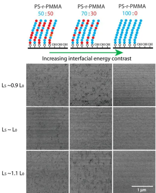
The investigation of the effects of both commensurability and chemical affinity on the registration of lamellar BCP has also been conducted in the stripes of polymer brush and a hydrophilic surface, by varying degree of commensurability (L0/Ls) and the ratio of PS-r-PMMA stripes on the substrate. The results of the SEM examination are shown in Fig.
31
3.4. It can be seen that the chemical affinity of the substrate improves the registration of the lamellar PS-b-PMMA. For chemically neutral stripes, PS-r-PMMA with ratio 50:50, the registration of the lamellar PS-b-PMMA is limited even when ~ 1. While for very high affinity (100% PS stripes), the defects are less pronounced and the window for good patterning registration is wider.
Fig. 3.4. SEM images of lamellae-forming PS-b-PMMA block copolymer films (L0 = 48 nm) on chemically
nanopatterned substrates as a function of LS (LS = 42.5 nm, 47.5 nm, and 52.5 nm) and composition of the
random-copolymer brush used to create the chemical pattern. The blue beads represent PS units and red beads represent PMMA units in the random block copolymer brush layer. Higher percentages of PS in the random block copolymer brush produce the higher chemical contrast of the surface patterns to PS-b- PMMA. Stronger chemical contrast favors replication of the underlying pattern [29].
32
Fig. 3.5. Process to create lithographically defined, chemically pre-patterned surfaces, and subsequent directed assembly. (A) Electron-beam lithography patterns at LS = L0 (left) and LS = 2L0 (right). (B)
Chemical contrast on the substrate after O2 plasma exposure on the e-beam–defined spots above. (C) Block
copolymer thin film. (D) Guided self-assembly in registration with the underlying chemical pattern [28]. The chemically-assisted pre-patterning process is shown in Fig. 3.5. First, rotary-stage electron beam lithography (EBL) is used to pattern the resist on top of the substrate. Rotary-stage EBL is chosen because it can define concentric layouts as required in hard disk media. Rotary-stage EBL is capable of fabricating grooves and bits on narrow pitch in concentric arrays with sub-50-nm range [30]. The schematic of rotary-stage EBL for creating concentric patterns on master template is given in Fig. 3.6.
33
In this process, the servo patterns are also written simultaneously with the data patterns. The continuous stage movement flyback lithography (CSFL) of rotary-stage EBL is capable of working in conjuction with a blankingless beam shift lithography (BLSL). This combination is very effective for fabricating various kinds of servo pattern elements. The layout of servo patterns can be seen in Fig. 3.7. Servo patterns are included on hard disks to enable the head element to read and write data at precise locations. We need to write the servo patterns only once in the master template, thus eliminating the need for servo writing in subsequent processes [22]. The disk is then exposed to oxygen plasma. Upon removal of the resist, a chemical contrast on the substrate is obtained.
Fig. 3.7. Servo pattern element write using the CSFL function. (a) Groove and dot, (b) dot and shifted elliptical dot, (c) groove and right-angled groove, and (d) different-length pits with various doses [30]. One important thing is that for a constant spin speed, the outer part of the media will
34
move with larger linear velocity. This implies that the data rate will be larger at the outer part. To resolve this, the bit size must vary with radius, i.e. larger bits for increasing radius. This requirement is easily accomplished in EBL system.
The bottom-up process begins by spin coating block copolymer (BCP) film onto the substrate. The ultimate resolution (R) expected in this process is basically proportional to the domain period D of BCP film. For BCP lithography purpose, we have to be in the strong segregation limit (N >> 10). In this region, the domain period is given
byD~aN2316, where a is the segment length, N is the overall number of segments (monomers), and is the Flory-Huggins interaction parameter. However, D is the period or the sum of the characteristic length scale of the BCP domains (PS and PMMA in our case). Since one domain is selectively etched away, the resolution will be the volume fraction of PS or PMMA (whichever is smaller) times the period. Theoretically, BCPs may form ordered periodic structures at the molecular scale ranging from 5-50 nm [31].
For BPM application purpose, it is required that the BCP lithography process has high resolution. Therefore, it is necessary to choose BCP with a high and decrease the block length (N) [32]. The resolution will also depend on etch selectivity between the blocks and subsequent pattern transfer process. It is required that the BCP has cylindrical or spherical morphologies. The morphology of BCP is determined by the volume fraction of each block, the relative chain-length differences of the constituent copolymers, and the processing condition. [33].
PS-b-PMMA has been widely used due to excellent chemical selectivity between PS and PMMA blocks, smooth microphase separation, the same glass-transition temperature, and a wide range of available solvents [34]. However, now PS-b-PDMS has also been considered since it has a high , giving a large driving force for microphase segregation, and a high chemical selectivity between the two blocks [35].
35
As shown in Fig. 3.8, the BCP film is annealed in vacuum to obtain cylindrical PMMA morphologies in PS matrix. The self assembly process of PS-b-PMMA is guided by the pre-patterned template, which is created by e-beam, to create a long-order pattern. The PMMA block will preferentially wet the spots exposed to oxygen plasma while the PS block will be slightly attracted to the background areas. The PMMA domains can then be selectively etched. This self-assembly process will increase the resolution of e-beam features by a factor of four and reduce the needed exposure time.
Fig. 3.8. Self-assembly of block-copolymer [9].
In HDD industry, we need to produce millions of disks. One method that provides simplicity, low cost, and high throughput is nanoimprint lithography (NIL). However, in imprinting such high volume of disks, the template can be easily damaged. Thus, template replication is essential to extend the template lifetime. Before proceeding to the media fabrication step, the obtained master template is first replicated by UV-NIL followed by a plasma-based transfer process into thousands of thin silica molds. These silica molds are then used in UV-NIL process to produce the disks.
3.3. Media Fabrication
To achieve high throughput, double-sided patterning is carried out using NIL. In UV-NIL process, as shown in Fig. 3.9, a layer of resist is sprayed on the substrate and the thin silica mold is brought into intimate contact with the substrate. To ensure intimate contact,
36
the template is bowed so that its center forms an initial contact with the center of the substrate. Then, capillary force will pull the entire template into conformal contact with the disk. Upon exposure to UV light, the imprinted resist will crosslink. Examples of patterned structures resulted from UV-NIL process are given in Fig. 3.10.
Fig. 3.9. UV-NIL process for patterned media [22].
37
The next step is then to transfer the pattern to a magnetic film. The magnetic film must be thin (<20 nm) for the write and read head to be able to resolve the high density islands. There are two generic approaches to this pattern transfer: [20]
(1) pre-patterning a substrate and subsequent deposition of a magnetic film;
(2) depositing a magnetic film and then dry-etching or milling it through a mask to define the islands.
It is also possible to use a lift-off process where the magnetic film is deposited onto the patterned resist and then the unwanted parts are dissolved to leave isolated magnetic islands. However, lift-off has not been particularly successful at sub-10 nm dimensions.
Fig. 3.11. Steps in the fabrication of patterned magnetic media [20].
The approach of pre-patterning a substrate, as shown in Fig. 3.11, has probably been the front running approach to date. The main motivations for using the pre-patterned substrate were:
(1) no good reactive ion etching (RIE) chemistry was known for the magnetic materials of interest;
(2) ion milling tends to result in redeposition;
(3) it would be necessary to clean all resist and redeposition to produce a clean, flyable disk;
38
(4) pre-patterning the substrate puts the patterning process earlier in the manufacturing process, and thus minimizing the impact of lower yields.
This approach has progressed significantly, with published patterned densities of 300 Gb/in2, the growth of thin perpendicular anisotropy layers, an understanding of the reversal processes, and static tester recording studies. However several challenges still exist. First, magnetic material in the trenches can give rise to noise. Second, the trenches also affect the stabilities in the flying. Moreover, there have been significant progresses in the RIE of magnetic materials and ion beam etching technology. So magnetic film etching is receiving renewed interest. At this time, the question of how to best pattern the magnetic film is still open.
For high-density recording, the head must fly within a close distance above the media. The magnetic spacing requirements for increasing areal density are illustrated in Fig. 3.12. BPM process creates topographies and thus imposing a high probability for the head to collide with the surface. Therefore, planarization scheme is introduced. First, a non-magnetic material is deposited by CVD or sputtering. Then, to obtain a planar disk surface, dry etching or milling can be used. Spin deposition and etch back can also be an option. However, it results in poor uniformity from the disk inside-diameter (ID) hole. Another alternative is using chemical mechanical polishing (CMP). CMP is a very mature process, but wet chemistry and consumables are problems. A planar disk is also advantageous in the overcoat process.
39
According to Hitachi and Seagate, the overall proposed schemes ensure high resolution and high throughput. Molecular Imprint Inc. claims that each of their NIL tools can produce millions of disks with only a single master template, as illustrated in Fig. 3.13. In their scenario, one master template can be faithfully replicated into 10,000 silica daughter templates, each of which can reproduce 10,000 disks. It is worthwhile to mention, however, that this estimation has not been proven in real industry.
40
4. Market Opportunity
4.1. Technology Supply Chain
In order to understand the importance of our technology, it is essential to locate the position of recording media in HDD process chain. The HDD supply chain is illustrated in Fig. 4.1.
Fig. 4.1. HDD supply chain [37].
A typical HDD manufacturing process starts with the fabrication of media, head, electronic components and motors. Through the various assembly steps, all the components are integrated into commercial products to be used in computers, telecommunication equipments, and other electronic devices. The BPM technology will play a role in the fabrication of the media. With the capability of meeting consumers‟ demand of high-density recording, an investment in this area is promising to gain significant profit.
The globalization of HDD supply chain can be seen in Fig. 4.2. It is important to note that the HDD media are mainly fabricated in USA, Malaysia, and Singapore.
41
Fig. 4.2. Globalization of HDD supply chain [38].
4.2. Competing Technologies
In order to achieve areal densities higher than PMR, besides using BPM as new recording media, we can use write-assist method to write in materials with a very high anisotropy. Several write-assist methods have been proposed, such as heat-assisted magnetic recording (HAMR), microwave-assisted magnetic recording (MAMR), and exchange-coupled composite (ECC) media [39]. All these write-assist methods are based on the same concept, i.e. enabling higher KU to enable smaller grain and thus better signal-to-noise ratio
(SNR).
4.2.1. Heat-Assisted Magnetic Recording
HAMR uses localized heat energy to reduce the medium coercivity. Its principle is similar to magneto-optical recording [40]. In this technology, we introduce write temperature as a new degree of freedom. Writing in media with higher anisotropy is made possible by
42
the coercivity is lowered below the available applied magnetic field. The written region is then rapidly frozen during the cooling process. The media can then be stably stored in room temperature. This writing process of HAMR is illustrated in Fig. 4.3.
Fig.4.3. Diagram of HAMR writing process [41].
However, there are several challenges faced by HAMR. First, at TC, the media grains are paramagnetic and do not respond to a field. This phenomenon is known as superparamagnetic trap. As the grains cool down from TC, the magnetization fluctuates rapidly. If the cooling rate after initial heating is too fast, the magnetization will be quenched in an arbitrary state. On the other hand, if the cooling rate is too slow, thermal erasure will increase due to heat that diffuse to neighboring bits [42]. Thus, temperature dependence of the medium magnetic properties, particularly around TC, is crucial for recording rate limitations and recording quality in HAMR. Factors that limit the rate of magnetization collapse and reformation along with the quality of the magnetization formation during freezing should be well understood. Recording simulations are needed to answer those questions.
The second and the ultimate challenge is breaking the diffraction limit of the laser source. In optical data storage, diode lasers have been widely used because they are inexpensive and capable of emitting high-power coherent light. The problem here is that those diode lasers available have wavelengths ranging from several hundred nanometers and longer.
43
State-of-the-art diode lasers are available at 375nm wavelength. However, to obtain storage densities beyond 1Tb/in2, we need spot size < 50nm [43]. The diffraction limit of far-field optics would provide achievable spot sizes that are too large. Thus, near-field optics has to be used [42]. In addition, an efficient technique must be provided for delivering large amount of light power to the recording medium and confining the light to sufficiently small optical spots. Finally, all the optical parts should be coupled for a complete optical system.
There are also challenges associated with building an integrated head for HAMR, lubricant, overcoat, and head-disk interface tribology due to high operating temperature.
4.2.2. Microwave-Assisted Magnetic Recording
In MAMR, an ac field with microwave frequency is applied along the easy axis opposite to the initial magnetization as shown in Fig. 4.4. The ferromagnetic resonance (FMR) frequency of the grain is determined by the externally applied reversing field and the anisotropy field of the grain. If the frequency of the ac field matches that of the grain, the system will absorb energy from the ac field. Above a certain switching field threshold, the magnetization precession will increase its precession angle and irreversibly gyro downwards within the duration of the pulsed reversing field. Thus, MAMR allows recording in the medium with anisotropy field higher than the maximum recording field [44]. As one of the proof of MAMR concept, reduction of switching field of single 20nm Co particle in the presence of an ac field has been demonstrated [45].
44
Proposed design of MAMR is illustrated in Fig. 4.5 (a). During the recording process, magnetization oscillation is generated in the field generating layer (FGL), as illustrated in Fig. 4.5 (b). Assuming that the magnetization of the perpendicular layer in the oscillating stack is along its anisotropy easy axis, the magnetization of the FGL is experiencing an effective magnetic field along the perpendicular axis. If the interlayer exchange field is greater than 4Ms, when the spin polarized current is zero, the magnetization will align itself in the perpendicular direction due to the damping torque. However, spin-polarized current will induce spin momentum transfer that generates a torque, termed spin torque, that is antiparallel to the damping torque. At sufficient current density, precession angle will be achieved. The angular frequency of the magnetization precession is Heffective. Current variation can tune the frequency directly over a very broad range, thus the frequency-current correlation is very important.
Fig. 4.5. (a) Schematic illustration of the ac field assisted perpendicular head design. (b) Illustration of magnetization precession of the field generating layer facilitated by the spin torque. int is the interlayer exchange coupling surface energy density, MS is the saturation magnetization, and is the thickness [44].
There are many advantages of MAMR, such as the direct coupling of assist energy into the magnetization mode and well understood theory behind it. However, MAMR also faces obstacles in its implementation. The device that is embedded in the head has not been proven to be technologically viable yet. Controlling the location of ac field and gradient is also a major obstacle in MAMR.
45
Moreover, according to J. Zhu et al., the optimum value for the switching field reduction is at field angle = 300. At this optimum angle, the minimum switching field is ~1/3 of the minimum switching field in the absence of ac field (Stoner-Wohlfarth value). Therefore, MAMR is only able to achieve about three times of perpendicular recording areal density (>1.5Tb/in2). In the most recent simulation, it was shown that a circular ac field of 2.5 kOe peak amplitude and 50 GHz frequency will enable an areal density of 1.88 Tb/in2 with a medium SNR above 18 dB. The highest obtainable density is 2.34 Tb/in2 at damping constant of 0.175 [20].
4.2.3. Exchange Coupled Composite Media
In ECC, a soft layer is used to assist the switching of the hard layer. Illustration of a grain in an ECC medium is given in Fig. 4.6. This write-assist process, known also as domain-wall-assisted switching, occurs only in the presence of an applied field [39]. The applied field will reverse the magnetization in the soft layer, creating a domain wall within each grain. This domain wall exerts pressure onto the hard layer and thus the switching field will be reduced. Very high anisotropy contrast between the layers is desired. Ideally, by using ECC, infinitely high anisotropy fields can be switched.
Fig. 4.6. Illustration of a grain in an ECC medium. It consists of a magnetically hard part and a magnetically soft part [39].
Fig. 4.7 depicts a schematic of the layer and magnetic structure for the proposed ECC media. [Co–PdSiO]n is used as the hard layer and FeSiO acts as the soft layer with a
non-46
magnetic PdSi interlayer between the hard and soft layer to tune the exchange coupling. SiO was doped into Pd layer to get magnetically isolated grains.
Advantages of ECC media compared to conventional continuous media are: 1) writability could be significantly improved without compromising its thermal stability; 2) the switching field of the media is much less sensitive to the angle dispersion (angle between the easy axis and applied field) compared to the perpendicular media. It is necessary to conduct further research to find out a better combination of hard and soft layer and optimize relevant magnetic parameters such as thermal stability and switching field to reach areal density beyond 1 Tb/in2.
Fig. 4.7. Basic structure of proposed ECC media [46].
4.2.4. Comparison among HAMR, MAMR, and ECC media
Among those three write-assist methods, HAMR is the most extensively studied. MAMR and ECC media are still in the infancy of their development to be currently considered as feasible manufacturing options. HAMR might enter the market before BPM, thus threatening the potential of commercializing BPM technology.
However, BPM can be combined with HAMR and ECC systems [24]. Magnetic isolation and small size distribution in BPM will enhance the HAMR and ECC areal density capabilities. By using a matrix with low heat conductivity, BPM can control heat
47
diffusion and thermal fluctuation in HAMR, thereby resolving the problem of erasure of information on adjacent tracks and recorded bit instability. Meanwhile, in ECC, the completely isolated magnetic grains in BPM will help totally eliminate the exchange coupling between magnetic grains. Thus, even if HAMR or ECC is established first, we can still use our media in their systems. The combination of HAMR with BPM is even projected to reach an areal density of ~100 Tb/in2 based on the thermal stability of known magnetic materials [47].
4.2.5. Outer Competitor
In the market, besides HDD, there are still many other types of storage disks. Solid-state drive (SSD) has especially gained commercial success due to its high speed, low noise, and low power consumption. However, as can be seen in Fig. 4.8, HDD offers the best areal density, capacity, and cost. Therefore, HDD shipment volume can be predicted to continue being on top as long as it can fulfill the increasing demand of areal density and capacity while maintaining its low cost.
48 4.3. Complementary Technologies
4.3.1. Head Technology
The recording and reading process in BPM is different from that of PMR. Reading the data faithfully from such small bits is challenging. For example, the head must fly within a reasonably close spacing from the media to resolve the high-density media, while at the same time maintain a safe distance to avoid collisions with the media due to protrusions and dust. To solve this problem, planarization process is inserted in the fabrication process. In the area of the read sensor, significant advances will be required for Tb/in2 applications. Challenges faced by read head are summarized in Table 4.1. The geometrical requirements for read head at high density are further listed in Table. 4.2.
Table 4.1. Read head challenges [4]. Small Geometry Track width
Shield spacing
High Sensitivity (mV/Oe) ΔV = i η (ΔR/R) R
Low Noise Johnson noise
Shot noise (TMR) Magnetic noise Design Constraints 50 Ω < R < 500 Ω
Temperature Rise Breakdown Voltage Spin Torque Instability Magnetic Self-Field
Table 4.2. Geometrical requirements for head for patterned media [4].
To fulfill these requirements, head technology has been evolving from CPP TMR to CPP GMR, as illustrated in Fig. 4.9. The structure of CPP TMR and CPP GMR are basically similar, except that the CPP GMR uses non-magnetic metal such as Cu instead of oxide as the interlayer between two ferromagnetic layers. The current CPP TMR sensor is based on spin-dependent tunneling mechanism. As the areal density increases, the sensor
![Fig. 1.1. Areal density trend [4] .](https://thumb-eu.123doks.com/thumbv2/123doknet/14383768.506807/11.918.154.767.548.915/fig-areal-density-trend.webp)
![Fig. 2.1. Hysteresis loop of a permanent magnet [10] .](https://thumb-eu.123doks.com/thumbv2/123doknet/14383768.506807/13.918.235.700.364.676/fig-hysteresis-loop-permanent-magnet.webp)
![Fig 2.4. Hysteresis behavior of a single-domain particle with the external field applied along (a) the easy axis, and (b) the hard axis [13] .](https://thumb-eu.123doks.com/thumbv2/123doknet/14383768.506807/15.918.264.661.135.324/hysteresis-behavior-single-domain-particle-external-field-applied.webp)
![Fig. 2.7. Disk coercivity versus areal density evolution [18] .](https://thumb-eu.123doks.com/thumbv2/123doknet/14383768.506807/17.918.158.746.190.599/fig-disk-coercivity-versus-areal-density-evolution.webp)
![Table 2.1. Examples of required lithography dimensions for patterned media [20] .](https://thumb-eu.123doks.com/thumbv2/123doknet/14383768.506807/19.918.165.751.487.725/table-examples-required-lithography-dimensions-patterned-media.webp)
![Fig. 2.10. MFM image of patterned media written by ring head. Black lines indicate a trajectory of the ring head [23].](https://thumb-eu.123doks.com/thumbv2/123doknet/14383768.506807/21.918.303.616.418.790/image-patterned-media-written-black-lines-indicate-trajectory.webp)
![Fig. 3.2. Functional layers of perpendicular recording medium. Layers are not to scale [27] .](https://thumb-eu.123doks.com/thumbv2/123doknet/14383768.506807/28.918.255.663.501.1028/fig-functional-layers-perpendicular-recording-medium-layers-scale.webp)
![Fig. 3.3. Chemically-assisted pattern generation [9] .](https://thumb-eu.123doks.com/thumbv2/123doknet/14383768.506807/30.918.175.733.124.469/fig-chemically-assisted-pattern-generation.webp)