HAL Id: hal-00591028
https://hal.archives-ouvertes.fr/hal-00591028
Submitted on 6 May 2011
HAL is a multi-disciplinary open access
archive for the deposit and dissemination of
sci-entific research documents, whether they are
pub-lished or not. The documents may come from
teaching and research institutions in France or
abroad, or from public or private research centers.
L’archive ouverte pluridisciplinaire HAL, est
destinée au dépôt et à la diffusion de documents
scientifiques de niveau recherche, publiés ou non,
émanant des établissements d’enseignement et de
recherche français ou étrangers, des laboratoires
publics ou privés.
Aircrafts
Daniela Dragomirescu, Michael Kraemer, Mohamed Mehdi Jatlaoui, Patrick
Pons, Hervé Aubert, Andrew Thain, Robert Plana
To cite this version:
Daniela Dragomirescu, Michael Kraemer, Mohamed Mehdi Jatlaoui, Patrick Pons, Hervé Aubert, et
al.. 60GHz Wireless Nano-Sensors Network for Structure Health Monitoring as Enabler for Safer,
Greener Aircrafts. Proceedings of SPIE- Advanced Topics in Optoelectronics Microelectronics and
Nanotechnologies, Aug 2010, Constanta, Romania. pp.78215. �hal-00591028�
60GHz Wireless Nano-Sensors Network for Structure Health
Monitoring as Enabler for Safer, Greener Aircrafts
D. DRAGOMIRESCU
1, 2, M. KRAEMER
1,2, M. M. JATLAOUI
1, 2, P. PONS
1,2,
H.AUBERT
1,2, A. THAIN
3, R.PLANA
1,21 CNRS; LAAS; 7, avenue du Colonel Roche, F-31077 Toulouse, FRANCE
2 University of Toulouse; UPS, INSA, INP, ISAE, LAAS; F-31077 Toulouse, FRANCE
3 EADS Innovation Work; 18, rue Maurice Terce, F-31025 Toulouse, FRANCE
ABSTRACT
The deployment of Wireless Sensors Network for Structure Health Monitoring will allow better maintenance of the aircraft and predictive diagnosis of the aircrafts in a long term approach. This paper presents our research on the design of wireless communicating nano-objects for Structure Health Monitoring in the aircrafts and the improvements bring by the nanotechnologies. The main challenges we address here are the design of ultra low power communicating circuits to enable high lifetime for the communicating nodes and their integration on flexible substrate to allow their deployment in difficult accessible places on the aircraft using conventional technologies. Other main issues are the choice of the communicating frequency which will allow a high number of communicating nodes in such a small area like the cabin of an aircraft and the choice of the network architecture.
Keywords: Structure Health Monitoring; Wireless Sensor Networks; Safer, smarter, green aircrafts;
60GHz communication; ultra low power 65nm CMOS circuits; Flexible substrate integration
1.
INTRODUCTION
The major driver for the aircraft industry development [1] nowadays is the eco-efficiency. That means the need of the development of future greener aircrafts with lowest carbon emission which pass by less weight in the aircraft while keeping the passenger comfort. The new generation of aircraft has to be also high performance while staying cost efficiency. That will be a global system challenge to develop the new generation aircrafts which can be solved only by a global system solution: rethink all the system architecture of the aircraft.
In this context, structure health monitoring (SHM) becomes a very important issue. The deploying of a whole sensor network on the structure of the aircraft is necessary. Nowadays, it is estimated that there are around 20000 aircrafts in activity and this number has to double by the end of 2025 and more than 1000 sensors are necessary for each one. The facility of sensor deployment becomes also a main issue. The introduction of sensor network for structure health monitoring will improve the maintenance system and will lead to safer aircrafts, which is another major topic together with eco-efficiency and also to lower airplane ticket cost for passengers. It is estimated that a decrease of 3% to 12% in the prices of airline tickets can be expected. Today the deployment of the sensors is limited by wired connections which lead to excess weight and carburant consumption (the major driver is eco-efficiency, greener aircrafts). The
wired sensor put also a huge problem of installation. The wireless solution, wireless sensor network, is imposed by these major constraints.
In the next paragraphs, we will first present the needs of structure health monitoring system, then the proposed network architecture, and we will focus on the ultra low power nano-technology circuits for 60GHz communications and the flexible substrate integration.
2.
STRUCTURE HEALTH MONITORING
The aeronautics is a very exigent industrial field with very high requirements in term of reliability. Compared with the ground transportation, the aircrafts accidents are one thousand times lower. It is estimated that two thirds of aircrafts failure could be eliminated or minimized by a high performance maintenance process and in the future a real time control of the flying aircraft. That shows the importance of the developing a structure health monitoring system. Structure health monitoring will reduce maintenance effort, increase aircrafts availability and can also reduce weight in the future. In the Airbus vision [1], it will be five generations, five main steps in the development of structure health monitoring systems. The “Generation 0” structure health monitoring systems, available since 2003 are dealing with structure testing application with benefits for structure analysis and testing. The “Generation 1“ structure health monitoring system recently available it consist on a off-board equipment with benefit for maintenance. The “Generation 2” structure health monitoring system will be on-board equipment and the benefit will be the maintenance, the diagnosis and weight saving component level. This system is expected by 2015 – 2018. The “Generation 3” structure health monitoring system will be a fully integrated system with benefit for the weight saving aircraft level, the maintenance and the availability and it will include predictive diagnosis. This system is expected by 2018 -2025. The “Generation 4” structure health monitoring system will be implemented on the aircrafts designed using smart materials, self-healing composite materials [2] [3]. The SHM system will diagnose the problem and the smart materials of the structure of the plane will be able to heal itself [2] [3]. This system will be expected in the very far future. In this paper we focus on the development of the 2nd and later the 3rd generation of structure health monitoring system. The main problem which has to be solved by the structure health monitoring system is the hard landing (Figure 1). The goals are to reduce the number of false reports, aiding the maintenance process and so reduce the aircraft schedule interrupts.
Fig. 1 Hard landing problem
The current maintenance process is initiated by the pilot by “feel” of the hard landing and then the maintenance team will verify the aircraft by visual inspection and recently using off-board equipment (Figure 2). The number of false report of hard landing is around 85% today [4] which lead to an important immobilization of the aircrafts. After deploying SHM system the maintenance process will change. The
pilot by “feel” of the hard landing will still initiate the inspection. Flight parameters and structure health monitoring sensor information will be used to predict load information in critical structure areas and recommend maintenance action. Theses informations will also aid maintenance actions. Using this SHM system will decrease the false report down to 5% and lead to an important increase in the availability of the aircraft.
Figure 2. Aircraft inspection after hard landing and maintenance process
In perspective, the SHM system will also allow to keep a component history report and lead to predictive diagnosis.
2.1 STRUCTURE HEALTH MONITORING SYSTEM REQUIREMENTS
It is clear now that we need to develop sensor networks for the SHM system. Wired sensor network can’t be used because of two main problems: difficulty of deployment and the increase of the weight of the aircraft. So, the wireless solution imposed itself. It has to be a modular communicating object which accepts different kind of sensors. The communication architecture has to support a very high number of communicating nodes. In such a small area like the aircraft cabin this will lead to carefully choice of the frequency to decrease the interferences. Moreover, no interference between this wireless sensor network and the passenger equipment are required. The data rate demand for this application is low or medium. Some measurements of the sensors has to be done in the same moment for all the sensors, so a synchronization measurement protocol is also needed. One important requirement is low power consumption as the wireless communicating objects has to work for years. The easy replacement of the autonomous power source, i.e. the battery, for this communicating nodes or the easy replacement of the all communicating node is also a strong requirement. The last major requirement is a complete
independent instrumentation with respect to the aircraft flying instrumentation. Nevertheless, this wireless sensor network has to be able to connect to aircraft network
All this requirements can be satisfied by COTS which are usually designed for medium number of nodes, without measurement synchronization protocol and communicating in the same bands as the passenger equipment which will lead at high interferences and can lead at huge security problem. Moreover, the COTS solutions are not so small and can’t be placed on curve surfaces and not so low power either. For all these raisons, we propose here a new architecture and technology for wireless communicating objects.
3.
ROBUST COMMUNICATION ARCHITECTURE
We propose to use the 60GHz band to short distance instrumentation and a flexible substrate integration which allow us to instrument event the difficult access areas on the aircraft. We have chosen the 60GHz band for many reasons. First of all, the transmission range at that frequency is short and the directivity of the wave is higher which will lead to lower interferences between the communicating nodes, a major requirement for our system: high number of communicating nodes in a small area. Second, the 60GHz is a free band. And the last, but not the least, the evolution of the CMOS technology in the nanotechnology area allow us today to design circuits in CMOS for 60GHz communication enabling low cost communicating nodes and a large scale production.
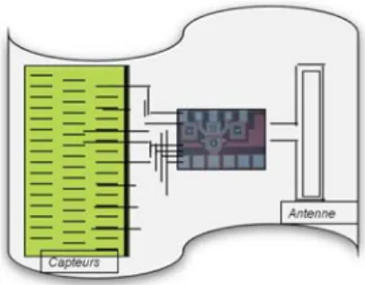
Figure 3 represents the communicating object as we proposed.
Figure 3. Wireless Communicating Node on Flexible Substrate
On the flexible substrate we will integrate the sensor element, the sensor signal processing, the communication circuit (digital baseband, RF front-end) and the antenna. The communicating node has to be seen as a modular platform which can include different kind of sensors.
The sensor can be done directly on the flexible substrate or on silicon and then reported on the flexible substrate. Different kind of sensors can be integrated on this substrate, as constraint gauge [5], crack wire or chemical / humidity detection sensor [6].
To assure very low power transceivers and low interferences we use Ultra Wide Band Impulse Radio (UWB-IR) communications which will be describe in the next section. The low power millimeter wave front end circuits design enabled by the use of CMOS nano-technology will be presented in section 5. The flexible substrate chooses here for the integration is a polyimide called Kapton. The detailed technological process set up and the technological breakthroughs are presented in [7].
From communication architecture point of view the next question to solve is how we can interrogate and retry data from the wireless communicating nodes. We propose a 3D heterogeneous integrated router scanner which will be placed in an area with more available energy (maybe wired powered). This router
will use the scanner principle to interrogate the communicating sensor nodes and realize the measurements as represented in Figure 4.
Figure 4. Architecture of router-scanner at 60GHz
The router will contain the same digital base band circuits and RF front end circuits developed in 65nm CMOS technology use a special concern for low power as the communicating node. On Figure 4, one can see that the router will scan the different communicating nodes. To realize the scanning function we will use our own MEMS RF phase shifters [8] (see Figure 5), coupled with array antenna on silicon. The smart antenna (phase shifter and antenna elements) will be integrated in 3D packaging on the top of the CMOS transceiver.
This new instrumentation architecture is original and takes profit from the properties of 60GHz communication channel to realize point to point measurements on short distances, with low sensitivity aux interferences.
4.
ULTRA WIDE BAND IMPULSE RADIO TRANSMISSION
The aeronautic application impose severe constrains for the reliability, the electromagnetic compatibility, the immunity of the interferences and the power consumption. All theses constraints lead us to choose to develop short distance wireless communications using ultra wide band impulse radio technique (UWB-IR) followed by a RF front-end at 60GHz. Figure 6 presents the principle of UWB-IR communications versus narrowband communications.
Figure 6. Ultra wide band impulse radio communications versus narrowband communications We demonstrate the very robust functioning of the UWB-IR in the context of our application by implementing a prototype of the full transceiver (emitter and receiver) completely reconfigurable on the FPGA with very good results [9]. A data rate of 125 Mbps was achieved [9], overcoming the state of the art.
The UWB-IR emitter developed is completely digital and able to generate the UWB-IR pulse, pulse modulation, spread spectrum and regulate the emitted power. The one bit digital emitter was implemented in ASIC using CMOS 65nm technology from ST Microelectronics. The fabricated UWB-IR emitter is presented in Figure 6 and the measurements show a maximum achievable data rate of 375Mbps for a band pass of 2.25GHz and a consumption of only 1.4pJ/bit. We notice here the achievement of this design: very low power consumption allowed by the nano-metric technology used and by a clever, simple design.
5.
60GHz LOW POWER, LOW COST DIRECT CONVERSION ARCHITECTUREAs presented in section 3, the 60GHz communications presents many major advantages for our wireless sensor network for SHM application. The complete System on Chip (SoC) architecture of the full transceiver, including UWB-IR base band and millimeter wave front end is presented in Figure 7.
Figure 7. System on chip architecture of the full transceiver to be implemented in nano-metric CMOS Different architectures for the millimeter wave front-end were studied [10], and for our application the best choice is the direct conversion architecture presented in Figure 8. The direct conversion architecture will lead to a small size transceiver, a very low power one and a low cost transceiver if implemented in CMOS. These three criteria are major criteria in Wireless Sensor Network for SHM (see section 2.1) Moreover, is an interesting challenge to design 60GHz completely CMOS circuits.
Figure 8. Direct conversion architecture of the 60Ghz front-end
Thanks to the nanotechnologies, the reduction of the gate size of the CMOS transistor in deep nano-metric circuits was possible. This leads to the increase of cutoff frequency in the silicon device, achieving the CMOS employment in this slice of market. After the 130nm generation, the CMOS device has prevailed the III-V group materials in particular for commercial applications. The Monolithic Microwave Integrated Circuits (MMICs) have been left to military and spatial applications. The Radio Frequency Integrated Circuits (RFICs) had become the new low cost commercial way.
We designed the main blocs of our transceiver in CMOS 65 nm from St Microelectronics. The major optimization criterion was the low power consumption of each bloc. The complete millimeter wave transceiver has to consume less than 100 mW.
The first step was the design of the inductances (see Figure. 9) with very good performances. [11],[12]
s=2µm w=3µm
100 µm
Figure 9. 60GHz Inductances designed in 65nm CMOS
We focus our design on the key blocs of the front-end. The Voltage Controlled Oscillator (VCO) at 60GHz was designed using a differential Colpitts architecture. The obtained VCO present very high power efficiency, the rapport between the output power and the DC power is 3.65, which is more than 3 times the value presented in the state of the art.
58 59 60 61 -6 -5 -4 -3 -2 -1 0 1 Pout ,d if f in d B m f in GHz
Pout,diff for VDD=1,2V, ID=20 mA
Pout,diff for VDD=1.0V, ID=16,5 mA
Figure 10. High power efficiency 60GHz VCO in 65nm CMOS
A new Low Noise Amplifier (LNA) was designed using two cascade stages and spiral inductances to minimize the size and the cost. The gain is 18.7dB and the power consumption is 8.5mW for 1V bias [13].
Figure 11. 65nm CMOS low power LNA
A dual-gate 60GHz direct up-conversion mixer with active IF balun in 65nm CMOS was also designed (Figure 12). A good conversion gain Gc= -4.1dB was measured for a DC power of 23mW [14].
Figure 12. Up-conversion mixer in 65nm CMOS
The use of the 65nm CMOS technology allow us to design low-power, low cost blocs at 60GHz.The next step is the complete integration of the very low power millimeter wave front-end which is under fabrication.
To obtain the communicating node of the Wireless Sensor Network (Figure 3), the CMOS transceiver will be added by Flip Chip on the flexible substrate (Figure 13). The 60GHz antenna will be designed directly on the flexible substrate. The choice of the flexible substrate has to be done very carefully to enable good radiation diagram for the antenna at 60GHz. 60GHz transmission lines between the transceiver and antenna has to be done. The Flip Chip of the 60GHz transceiver on the flexible substrate is a new way to package circuits at 60GHz. The small dimension of the pads, the 60 GHz connections and the low temperature process impose new technological methods described in [7].
.
Figure 13. Kapton-100HN flexible substrate ready for the Flip Chip report of the 60GHz blocs
6.
CONCLUSION
Structure Health Monitoring is a main concern nowadays to build safer, greener aircrafts. The main requirements of the wireless communicating nodes are low interferences with passenger equipment and between communicating nodes, high reliability, low power and low cost. The capacity of placing these nodes on the all aircraft surfaces, including non planar one is a major request. We presented in this paper new wireless sensor network architecture, circuits and packaging able to answer the SHM requirements. The 60GHz communication will allow high number of nodes in such a small area like the aircraft cabin. The design of low power and low cost 60GHz transceiver is enabled by the use of nano-metric CMOS technology. The complete integration of the sensor communicating node was done on flexible substrate. The achievement of the wireless communicating nodes for SHM is enabled by the use of the nanotechnologies in the design of the transceivers, antenna and integration on flexible substrate.
Acknowledgments
This work has been supported by the French National Research Agency (ANR) in the frame of its program” Recherche Technologique Nano-INNOV/RT” (NANOCOMM project n°ANR-09-NIRT-004).
REFERENCES
[1] H. Rosner, Airbus, “Smart structures contribution to Airbus aircraft efficiency”, International Workshop on Structural Health Monitoring, September 2009, Stanford, USA
[2] Trosk et al., J.R. Soc. Interface , 2007 [3] White et al., Nature, 2006
[4] J.Young, Boeing, “Structural Health Management, an Evolutionary Journey” International Workshop on Structural Health Monitoring, September 2009, Stanford, USA
[5] L.Ressier, E.Palleau, C.Garcia, G.Viau et B.Viallet, “How to control AFM nanoxerography for the template monolayered self-assembly of 2 nm colloidal gold nanparticules”, IEEE Trans. on Nanotechnology no.4, pp. 487-491, 2009
[6] P. Temple Boyer, A. Benyahia, W. Sant, M.L. Pourciel-Gouzy, J. Launay, A. Martinez : "Modelling of urea-EnFETs for haemodialysis applications", Sensors and Actuators, vol 131/2 (2008), p.525-532
[7] M.M.Jatlaoui, D.Dragomirescu, S.Charlot, P.Pons, H.Aubert, R.Plana “Heterogeneous integration of Communicating Nano-Objects on Flexible Substrate” , Proceedings of ATOM-N 2010
[8] V.Puyal, D.Dragomirescu et al. “Frequency Scalable Model for MEMS Capacitive Shunt Switches at Millimeter Wave Frequencies”, IEEE Transaction on Microwave Theory and Techniques, vol.57, issue 11, pp. 2824 – 2833 [9] A.Lecointre, D.Dragomirescu, R.Plana, “Largely reconfigurable impulse radio UWB transceiver”, Electronics
Letters, vol.46, issue: 6, pp. 453-455, year 2010
[10] M.Kraemer, A.Lecointre, D.Dragomiresc, R.Plana, “Architecture Considerations for 60 GHz Pulse Transceiver Front-ends”, Proceedings of 30rd International Conference on Semiconductors 2007 (CAS2007), pp.425-428, Sinania, Romania
[11] Kraemer, M.; Dragomirescu, D., Plana, R.: « Accurate Electromagnetic Simulation and Measurement of Milimeter-wave Inductors in Bulk CMOS Technology », 10th Topical Meeting on Silicon Monolithic Integrated
Circuits in RF Systems, 2010
[12] Kraemer, M.; Dragomirescu, D.; Rumeau, A., Plana, R.: «On the De-embedding of Small Value Millimeter-wave CMOS Inductor Measurements », 5th German Microwave Conference 2010, p. 194-197
[13] Kraemer, M.; Dragomirescu, D., Plana, R.: « A low-power high-gain LNA for the 60 GHz band in a 65 nm CMOS technology », Proc. Asia Pacific Microwave Conf. APMC 2009, p. 1156-1159
[14] Kraemer, M.; Dragomirescu, D., Plana, R.: « A Dual-Gate 60GHz Direct up-Conversion Mixer with Active IF Balun in 65nm CMOS », IEEE International Conference on Wireless Information Technology and Systems, 2010