HAL Id: hal-03044230
https://hal.archives-ouvertes.fr/hal-03044230
Submitted on 11 Dec 2020
HAL is a multi-disciplinary open access
archive for the deposit and dissemination of
sci-entific research documents, whether they are
pub-lished or not. The documents may come from
teaching and research institutions in France or
abroad, or from public or private research centers.
L’archive ouverte pluridisciplinaire HAL, est
destinée au dépôt et à la diffusion de documents
scientifiques de niveau recherche, publiés ou non,
émanant des établissements d’enseignement et de
recherche français ou étrangers, des laboratoires
publics ou privés.
Reducing AFDX jitter in a mixed NoC/AFDX
architecture
Laure Abdallah, Jérôme Ermont, Jean-Luc Scharbarg, Christian Fraboul
To cite this version:
Laure Abdallah, Jérôme Ermont, Jean-Luc Scharbarg, Christian Fraboul. Reducing AFDX jitter in a
mixed NoC/AFDX architecture. IEEE 14th International Workshop on Factory Communication
Sys-tems (WFCS 2018), Jun 2018, Imperia, Italy. pp.1–4, �10.1109/WFCS.2018.8402375�. �hal-03044230�
Reducing AFDX jitter in a mixed NoC/AFDX
architecture
Laure Abdallah, J´erˆome Ermont, Jean-Luc Scharbarg, Christian Fraboul
Universit´e de Toulouse/IRIT/Toulouse INP-ENSEEIHT 2 rue Charles Camichel 31000 Toulouse
Email:{firstname.name}@enseeiht.fr
Abstract—Current avionics architecture are based on an
avionics full duplex switched Ethernet network (AFDX) that
interconnects end systems. Avionics functions exchange data
through Virtual Links (VLs), which are static flows with bounded
bandwidth. The jitter for each VL at AFDX entrance has to
be less than 500 µs. This constraint is met, thanks to end
system scheduling. The interconnection of many-cores by an
AFDX backbone is envisionned for future avionics architecture.
The principle is to distribute avionics functions on these
many-cores. Many-cores are based on simple cores interconnected by
a Network-on-Chip (NoC). The allocation of functions on the
available cores as well as the transmission of flows on the NoC
has to be performed in such a way that the jitter for each VL
at AFDX entrance is still less than 500 µs. A first solution has
been proposed, where each function manages the transmission
of its VLs. The idea of this solution is to distribute functions
on each many-core in order to minimize contentions for VLs
which concern functions allocated on different many-cores. In
this paper, we consider that VL transmissions are managed by
a single task in each many-core. We show on a preliminary case
study that this solution significantly reduces VL jitter.
I. INTRODUCTION
Aircrafts are equipped with numerous electronic equipment.
Some of them, like flight control and guidance systems,
provide flight critical functions, while others may provide
assistance services that are not critical to maintain
airworthi-ness. Current avionics architecture is based on the integration
of numerous functions with different criticality levels into
single computing systems (mono-core processors) [6]. Such
an architecture is depicted in Figure 1. Computing systems are
interconnected by an AFDX (Avionics Full Duplex Switched
Ethernet) [1]. The End System (ES) provides an interface
between a processing unit and the network.
The continuous need for increased computational power
has fueled the on-going move to multi-cores architectures
in hard real-time systems. But, multi-cores architectures are
based on complex hardware mechanisms, such as advanced
branch predictors whose temporal behavior is difficult to
master. Many-cores architectures are based on simpler cores
interconnected by a Network-on-Chip (NoC). These cores
are more predictable [9]. Thus, many-cores are promising
candidates for avionics architecture.
A typical many-cores architecture provides Ethernet
inter-faces and memory controllers. For instance, Tilera Tile64 has
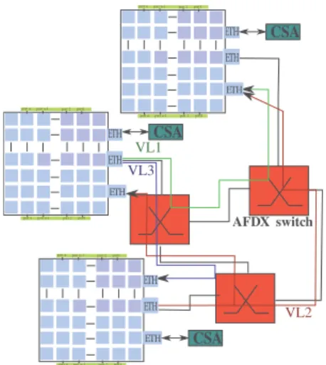
Fig. 1: An AFDX network.
3 Ethernet interfaces and 4 memory controllers [10], Kalray MPPA has 8 Ethernet interfaces and 2 memory controllers [5]. An envisioned avionics architecture is depicted in Figure 2. A set of many-cores are interconnected by an AFDX back-bone, leading to a mixed NoC/AFDX architecture. Avionics functions are distributed on these many-cores. Communica-tions between two funcCommunica-tions allocated on the same many-cores use the NoC, while the communications between two functions allocated on different many-cores use both the NoC and the AFDX. Main constraints on this communication are the following: (1) end-to-end transmission delay has to be upper-bounded by an application defined value, (2) frame jitter at the ingress of the AFDX network has to be smaller than a given value (typically 500 µs). In single core architectures the latter constraint is enforced by the scheduling implemented in the End System. In many-cores architectures, frame jitter mainly depends on the delay variation between the source core and the source Ethernet interface. This variation is due to two factors. First, the frame can be delayed on the NoC by other frames transmitted between avionic functions. Second, the Ethernet controller can be busy, transmitting another frame. [2] proposes a mapping strategy which minimizes the first factor, i.e. the variation of this NoC delay. Each core is allocated at most one function. Each VL is managed by its source function. In this paper, we mainly address the second factor. We propose a static scheduling of Ethernet transmissions, based on a table. Each transmission is allocated a periodic slot. The scheduling is managed by a dedicated core.
The remainder of the paper is as follows. Section II intro-duces current AFDX and NoC architectures. Section III ex-plains the addressed problem. The new approach is described in Section IV. Section V presents preliminary results on a case study. Finally, Section VI concludes with some future works.
Fig. 2: A mixed NoC/AFDX architecture
II. SYSTEM MODEL
We summarize the main features of both an AFDX flows and many-cores considered in this paper.
A. AFDX flows
A VL defines a unidirectional connection between one source function and one or more destination functions. Each VL is characterized by two parameters:
• Bandwidth Allocation Gap (BAG). Minimal time
in-terval separating two successive frames of the same VL. Value from 1 to 128 ms.
• Lmin andLmax.Smallest and largest Ethernet frame, in
bytes, transmitted on the VL.
In current architectures, each ES performs a traffic shap-ing for each VL to control that frames are transmitted in accordance with BAG and authorized frame size. The queued frames, which are ready to be transmitted, are then selected depending on a strategy configured in the VL scheduler. There-fore, it is possible that more than one VL has a packet ready and eligible for transmission. In this case, a queuing delay (jitter) is introduced. This jitter, computed at the transmitting ES, is the time between the beginning of BAG interval and the first bit of the frame to be transmitted in that BAG. This jitter must not be greater than 500µs.
B. NoC Architecture and Asumptions
In this paper, we consider a Tilera-like NoC architecture,
i.e.a 2D-Mesh NoC with bidirectional links interconnecting a
number of routers. Each router has five input and output ports. Each input port consists of a single queuing buffer. The routers at the edge of the NoC are interconnected to the DDR memory located north and south of the NoC via dedicated ports. The first and last columns of the NoC are not connected directly to the DDR. Besides, the routers at the east side connects the cores to the Ethernet interfaces via specific ports. Many applications can be allocated on a NoC. Each application is composed of a number of tasks, where one core executes only one task. These tasks do not only communicate with each other (core-to-core flows), but also with the I/O interfaces,
i.e. the DDR memory and Ethernet interfaces (core-to-I/O flows). These flows are transmitted through the NoC following wormhole routing [8], an XY policy and a Round-Robin arbitration. Besides, a credit-based mechanism is applied to control the flows. A flow consists of a number of packets, corresponding to the maximal authorized flow size on the NoC. Indeed, a packet is divided into a set of flits (flow control digits) of fixed size (typically 32-bits). The maximal size of a NoC packet is of 19 flits as in Tilera NoC. The wormhole routing makes the flits follow the first flit of the packet in a pipeline way creating a worm where flits are distributed on many routers. The credit-based mechanism blocks the flits before a buffer overflow occurs. The consequence of such a transmission model is that when two flows share the same path, if one of them is blocked, the other one can also be blocked. Thus, the delay of a flow can increase due to contentions on the NoC. The Worst-case Traversal Time (WCTT) of a flow can be computed using different methods proposed in the
literature [7]. In this paper, we choose RCN oC [3] to compute
the WCTT as it leads to tightest bounds of delays compared to the existing methods on a Tilera-like NoC. This method considers the pipeline transmission, and thus computes the maximal blocking delay a flow can suffer due the contentions with blocking flows.
III. PROBLEM STATEMENT
Both incoming and outgoing flows are transmitted on the NoC. The mapping strategy has a big impact on the delay of these flows on the NoC, since this delay depends on the core where source and destination tasks are mapped and on contentions encountered by flows on their path. Authors of
[4] have proposed a mapping strategy called MapIO that
minimizes the delay of incoming Ethernet flows.
However, this mapping strategy does not consider the out-going I/O flows. Actually, an outout-going I/O flow is transmitted following three steps: (1) A core sends data to the nearest port of DDR memory, (2) then it sends a DMA command to the Ethernet interface on a separate network. This DMA command indicates the placement of data in the DDR memory, and it is stored into a DMA command FIFO queue. (3) When the Ethernet interface executes the DMA command, data packets are then sent from the same port of DDR memory to the same Ethernet interface. The packets of an outgoing I/O flow will incur a contention with different types of communications on the NoC which could lead to a jitter.
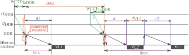
Let us illustrate the delays of these steps with the example in
Figure 3. Two VLs V L1 and V L2 are respectively generated
by tasks t1DDR and t2DDR. At the begining of V L1 first
BAG period, t1DDR sends V L1 data to the nearest port of
DDR memory. This transmission can take up to W CT TtoDRR.
Step 2 (transmission of the DMA command to the Ethernet interface) is done after this worst-case delay. Thus step 1 duration is constant and does not generate any jitter. Similarily, step 2 duration is assumed to be constant, since the DMA com-mand is sent on a separate network. Thus all the jitter comes from step 3 (transmission of the data from DRR memory
t1DDR t2DDR DDR Ethernet Interface WCTTToDDR command executed D MA co mman d VL1 d1 BAG Jitter VL2 VL1 WCTTToDDR Jitter d2 d dVL2
Fig. 3: A possible transmission on a given VL.
to the Ethernet interface. Considering V L1 first BAG period
in Figure 3, the jitter is the delay d1 of this transmission, which is between 0 and its worst-case duration. The jitter can
be much higher. Indeed, for V L1 second BAG period, the
Ethernet interface is busy with V L2 when it receives V L1
DMA command. The delay due to V L2 has to be added to
the jitter, leading to an overall value of d+ dV L2+ d2.
The authors of [2] extended the MapIO strategy. Several
rules have been defined to minimize the delay of outgoing I/O flows on the NoC, i.e. d, d1 and d2 in Figure 3. One rule consists in allocating the source tasks of outgoing I/O flows in columns with minimum DDR usage. These DDR flows can be delayed by other inter-core flows. Thus, rules map tasks on cores in order to minimize the number of such flows going in the same direction as DDR ones. Therefore, a rule minimizes the number of flows that can delay an outgoing I/O flow on its path. The solution considered in this paper is based on the mapping strategy in [2]. The goal is to avoid that the Ethernet interface is busy when it receives a DMA command (like for
V L1 second period in Figure 3).
IV. ADEDICATED CORE FOR OUTGOINGI/OFLOWS
We propose to dedicate a specific core of the NoC to the transmission of VL through the Ethernet interface. The idea
is to execute only one task tDDR for all the applications. This
task can be executed on every free node of the NoC since the transmission of the command of the DDR uses another internal network. For the implementation, we consider that this task is the only task of a function named COM1. This function is then mapped on the NoC using the considered mapping strategy.
The behaviour of the task tDDR is as follow:
1) Reception of a message from the final task of the function: the data that need to be sent are in the DDR. In such a way, we do not change the behaviour of the functions presented in section II-B. The transmission of the message is constant and can be considered as a part of the execution time of the sending task of the function. 2) Transmission of a DDR command to the DDR. The corresponding data are then transmitted from the DDR to the Ethernet interface.
In this paper, we consider that the schedule of the DDR commands, and so the VLs sent by the functions, can be done by using a scheduling table. The goal of this method is to reduce the jitter induced by the transmission of other VLs from the memory to the Ethernet interface through the NoC and the transmission of these VLs through the Ethernet interface. The considered scheduling table is composed of slots of 31.25µs.
port 1 port 2 port 3 port 4 port 5 4 5 6 7 3 2 1 0 5 6 7 0 1 2 3 4 (10,0) (0,0) 8 9 10 8 9 10 port 11 port 12 port 13 port 14 port 15 port 16 port 17 port 18 port 6 port 7 port 8 FADEC7 tf3 tf2 tf0 tf4 tf6 tf5 tf1 th6 th7th8 th4 th1 th0 th2 th3 th5 th9 HM10 (0,5) th11 th6 th7 th10 th9 th8 th4 th1 th0 th2 th3 th5 th12 th13 th14 th15 HM16 th6 th7 th8 th4 th1 th0 th2 th3 th5 HM9 tf6 tf7 tf1 tf0 tf4 tf3 tf5 tf2 tf8 tf10 tf9 FADEC11 FADEC13 tf6 tf7 tf0 tf1 tf4 tf3 tf5 tf2 tf8 tf10 tf9 tf11 tf12 th9 th8 th7 th10 th11 th6 th4 th1 th2 th0 th5 th3 HM12 th9 th8 th7 th10 th6 th4 th1 th2 th0 th5 th3 HM11 tDDR port1 port2 port3 port4 port5 4 5 6 7 3 2 1 0 5 6 7 0 1 2 3 4 (10,0) (0,0) 8 9 10 8 9 10 port11 port12 port13 port14 port15 port16 port17 port18 port6 port7 port8 FADEC7 tf3 tf2 tf0 tf4 tf6 tf5 tf1 th6 th7 th8 th4 th1 th0 th2 th3 th5 th9 HM10 (0,5) th11 th6 th7 th10 th9 th8 th4 th1 th0 th2 th3 th5 th12 th13 th14 th15 HM16 th6 th7 th8 th4 th1 th0 th2 th3 th5 HM9 h14 h14 h15 h15 FADEC13 tf6 tf7 tf0tf1 tf4 tf3 tf5 tf2 tf8 tf10 tf9 tf11 tf12 th9 th8 th7 th10 th11 th6 th4 th1 th2 th0 th5 th3 HM12 th9 th8 th7 th10 th6 th4 th1 th2 th0 th5 th3 HM11 tf6 tf7 tf1 tf0 tf4 tf3 tf5 tf2 tf8 tf10tf9 FADEC11 11 11 HM HM77 th3 th4 th5 th6 th0 th1 th2 7 th5h5 tth6h6 th0h0 h1 h2 tDDR
Fig. 4: Mapping 8 (left) and 9 (right) applications on a 10x10
many-core using ex M apIO.
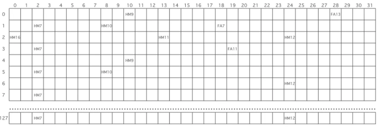
The global duration of the table is 128 ms. So the number of slots is 4096. The table is composed of 128 lines of 1 ms, each line contains 32 slots. A set of slots is allocated to each VL sent by the applications by considering the BAG duration: a VL will obtain a slot at exactly each BAG. Such a scheduling is represented in Table I. In this example, we denoted by the name of the application the slot when the corresponding VL should be sent. As an example, a VL from the application
HM7 has a BAG duration equal to 2 ms. It can be located
in column 1 of lines 1, 3, . . . , 127. In the same manner, VL
from the application HM9 has a BAG of 4 ms and is located
in column 10 of lines 0, 4, 8, . . . , 124.
This scheduling guarantees that the VLs are sent from the memory to the Ethernet interface at different times, leading to a reduction of the jitter induced by the transmission of other VLs. In such a way, the only delay that a VL can suffer when it is transmitted from the DDR is due to the interferences from the transmission of internal communications through the NoC that share the same path as the VL.
V. PRELIMINARY CASE STUDY
The considered case study is composed of critical and non critical applications:
• Full Authority Digital Engine (FADEC) application:
It controls the performance of the aircraft engine. It receives 30 KBytes of data from the engine sensors via an Ethernet interface and sends back 1500 Bytes of
data to the engine actuators. The application FADECn
is composed of n tasks denoted tf 0 to tf n−1. tf n−1 is
dedicated to send the commands to the engine actuators
via the Ethernet interface. Except tf n−1, all other tasks
exchange 5 KBytes of data through the NoC. They also
send 5 KBytes of data to tf n−1.
• Health Monitoring (HM) application:It is used to
rec-ognize incipient failure conditions of engines. It receives through an Ethernet interface, a set of frames of size 130 KBytes and sends back 1500 bytes of data actuators.
The application HMn is composed of n tasks, denoted
th0 to thn−1. The last task thn−1 is dedicated to send
the data actuators to the Ethernet interface. The task thi
sends 2240 bytes of data to thi+1through the NoC, with
i∈ [0, n − 2]. All these tasks finish their processing by
TABLE I: Scheduling table of the VL sent by each application. 0 1 2 3 4 5 6 7 8 9 10 11 12 13 14 15 16 17 18 19 20 21 22 23 24 25 26 27 28 29 30 31 0 HM9 FA13 1 HM7 HM10 FA7 2 HM16 HM11 HM12 3 HM7 FA11 4 HM9 5 HM7 HM10 6 HM12 7 HM7 127 HM7 HM12 ………
TABLE II: Maximum jitter experienced by the transmission of VL, in µs
8 applications 9 applications distributed tDDR 436.5 558.3
one tDDR 77,5 80,9
FADEC applications are critical, while HM applications are non-critical. Figure 4 shows the mapping of 8 applications (3 FADEC and 8 HM) and 9 applications (3 FADEC and 6 HM) on the NoC.
Preliminary results are shown in Table II. Distributed tDDR
corresponds to the solution described in Section III. The mapping strategy of [2] has been defined to improve the transmission of outgoing flows. Then, it allows a significant reduction of the jitter, leading to a jitter value less than 500µs for an 8 applications mapping. But, the jitter is still greater than 500µs when mapping 9 applications. As expected, the solution proposed in the paper significantly reduces the jitter of the VLs. The jitter becomes lower than 100µs when mapping both 8 and 9 applications on the NoC.
This proposed solution schedules the transmission of frames of a given VL but the frames have to wait for their slot. As an
example, VL from HM10in Table I has to be sent at slot 8 of
line 2. If the message from the application to the transmission node arrives after the beginning of this slot, the VL has to wait for the slot 8 of line 5. One solution to overcome this waiting time is the overbooking of the slots, for instance one slot each milliseconds for a VL with a BAG of 4ms.
VI. CONCLUSION
In this paper, we proposed to replace the mono-core pro-cessors in avionics architecture by a NoC-based many-cores architecture. Thus, End Systems are replaced by many-cores. Different mapping strategies have been used in order to minimize the jitter provided by the interferences on the NoC. The jitter increases by increasing the size of the NoC and the number of functions and we show on a realistic avionics architecture that it leads to an excess of the maximum allowed jitter. The main contribution of the paper is that it proposes a
new VL transmission strategy which considers one dedicated node in the many-core architecture to shape the traffic and schedules the outgoing I/O flows. The preliminary results show that the jitter is significantly reduced and only depends on the interferences that can occur on the transmission path between the DDR and the I/O interface.
Further works concern how to construct the scheduling table in order to take into account the overbooking of the slots.
REFERENCES
[1] Aeronautical Radio Inc. ARINC 664. Aircraft Data Network, Part 7: Avionic Full Duplex Switched Ethernet (AFDX) Network, 2005. [2] Laure Abdallah, J´erˆome Ermont, Jean-Luc Scharbarg, and Christian
Fraboul. Towards a mixed NoC/AFDX architecture for avionics applica-tions. In IEEE 13th International Workshop on Factory Communication Systems, WFCS 2017, Trondheim, Norway, May 31 - June 2, 2017, pages 1–10, 2017.
[3] Laure Abdallah, Mathieu Jan, J´erˆome Ermont, and Christian Fraboul. Wormhole networks properties and their use for optimizing worst case delay analysis of many-cores. In 10th IEEE International Symposium on Industrial Embedded Systems (SIES), pages 59–68, Siegen, Germany, June 2015.
[4] Laure Abdallah, Mathieu Jan, J´erˆome Ermont, and Christian Fraboul. Reducing the contention experienced by real-time core-to-i/o flows over a tilera-like network on chip. In Real-Time Systems (ECRTS), 2016 28th Euromicro Conference on, pages 86–96. IEEE, 2016.
[5] Benoˆıt Dupont de Dinechin, Duco van Amstel, Marc Poulhi`es, and Guillaume Lager. Time-critical computing on a single-chip massively parallel processor. In Proc. of the Conf. on Design, Automation & Test in Europe (DATE’14), pages 97:1–97:6, 2014.
[6] RTCA DO. 178c. Software considerations in airborne systems and equipment certification, 2011.
[7] Thomas Ferrandiz, Fabrice Frances, and Christian Fraboul. Using Network Calculus to compute end-to-end delays in SpaceWire networks. SIGBED Review, 8(3):44–47, 2011.
[8] Prasant Mohapatra. Wormhole routing techniques for directly connected muti-computer systems. ACM Computer Survey (CSUR), 30(3):374–410, September 1998.
[9] Vincent N´elis, Patrick Meumeu Yomsi, Lu´ıs Miguel Pinho, Jos´e Carlos Fonseca, Marko Bertogna, Eduardo Qui˜nones, Roberto Vargas, and An-drea Marongiu. The Challenge of Time-Predictability in Modern Many-Core Architectures. In 14th Intl. Workshop on Worst-Case Execution Time Analysis, pages 63–72, Madridr, Spain, July 2014.
[10] David Wentzlaff, Patrick Griffin, Henry Hoffmann, Liewei Bao, Bruce Edwards, Carl Ramey, Matthew Mattina, Chyi-Chang Miao, John F. Brown III, and Anant Agarwal. On-chip interconnection architecture of the tile processor. IEEE Micro, 27(5):15–31, 2007.