HAL Id: hal-00670144
https://hal.archives-ouvertes.fr/hal-00670144
Submitted on 14 Feb 2012
HAL is a multi-disciplinary open access archive for the deposit and dissemination of sci-entific research documents, whether they are pub-lished or not. The documents may come from teaching and research institutions in France or abroad, or from public or private research centers.
L’archive ouverte pluridisciplinaire HAL, est destinée au dépôt et à la diffusion de documents scientifiques de niveau recherche, publiés ou non, émanant des établissements d’enseignement et de recherche français ou étrangers, des laboratoires publics ou privés.
5x1 Linear Antenna Array for 60 GHz Beam Steering
Applications
Mikko Kyrö, Diane Titz, Veli-Matti Kolmonen, Sylvain Ranvier, Patrick Pons,
Cyril Luxey, Pertti Vainikainen
To cite this version:
Mikko Kyrö, Diane Titz, Veli-Matti Kolmonen, Sylvain Ranvier, Patrick Pons, et al.. 5x1 Linear Antenna Array for 60 GHz Beam Steering Applications. European Conference on Antennas and Propagation, Apr 2011, Rome, Italy. 4 p. �hal-00670144�
5 x 1 Linear Antenna Array for 60 GHz Beam
Steering Applications
Mikko Kyrö*, Diane Titz+, Veli-Matti Kolmonen*, Sylvain Ranvier*, Patrick Pons◊ Cyril Luxey+, and Pertti Vainikainen*
*Aalto University School of Electrical Engineering, Department of Radio Science and Engineering, SMARAD
P.O. Box 13000, FI-00076 Aalto, Finland [email protected]
+ LEAT-CREMANT-CNRS, University of Nice-Sophia-Antipolis
250, rue Albert Einstein, 06560 Valbonne, France [email protected]
◊ LAAS-CNRS, University of Toulouse,
F-31077 Toulouse, France
Abstract— This paper presents a design process and simulation
results of a 5 x 1 linear antenna array with phase shifters for 60 GHz beam steering applications. The antenna array has been designed using a membrane process in order to achieve high radiation efficiency and good radiation characteristics. The same process can be used to manufacture Micro-Electro-Mechanical Systems (MEMS) switches and phase shifters. The maximum gain of the developed antenna array is 9.0 dBi and the radiation efficiency is 87 %. The array consists of 5 equally spaced monopole antennas which each has a gain of 3.2 dBi. The reflection coefficient of the antenna elements is better than -13.5 dB at the desired frequency range from 57 to 64 GHz and the minimum isolation between the adjacent antenna elements is 10.4 dB. The phase shifter which is used for steering the beam of the antenna array has been implemented with MEMS switches and switched transmission lines. The phase shifter enables a phase shift from -80° to +80° by 20° steps. The losses of the phase shifters are less than 2 dB. The results reveal that the membrane technology is a good option for implementing beam steering antenna systems for 60 GHz communications applications.
I. INTRODUCTION
Multiantenna techniques such as Multiple-Input and Multiple-Output (MIMO) and beam steering can be used to increase data transmission rates or reliability of wireless communications systems [1]. The beam steering has been considered as one of the key technologies for 60 GHz communication e.g. by the IEEE 802.11ad standardization working group. It has two advantages compared to single antenna systems: increased gain due to use of antenna array and possibility to reduce interference by steering the beam to the desired direction. Drawbacks are increased complexity and power losses in the phase shifters and antenna array feeding structure. The phase shifters are used for steering the beam of the antenna array. Several phased antenna array designs have been already introduced in the literature for 24 GHz in [2], and for 60 GHz in [3] - [5]. In [2] the phase shifting is done in LO domain. In [3] the phase shifters have been realized with a Butler matrix network, in [4] with a Rotman lens and in [5] with Micro-Electro-Mechanical Systems (MEMS) technology.
At millimeter wave frequencies antennas which are manufactured on normal substrate materials have often low radiation efficiency and poor radiation properties. This is mainly due to surface waves which store energy inside the substrate and losses of the substrate. The efficiency of the antenna can be increased by replacing the substrate with a thin membrane layer. The use of membrane provides reduction of losses, dispersion effects as well as suppression of higher order substrate modes. In addition, the manufacturing costs of the membrane processed antennas are relatively low. Previous designs using membrane structure are Yagi-Uda antennas for 60 GHz and 77 GHz frequency ranges [6], supported end-fire antennas for 45 GHz [7] and membrane-supported double folded slot antennas for 60 GHz [8]. This paper combines beam steering techniques and a membrane supported antenna array for the first time at 60 GHz. The antenna array has been designed to operate at the unlicensed frequency band from 57 to 64 GHz for short range very high data rate communications applications.
The remainder of the paper has been organized as follows; Section II presents the structure of the designed antenna array together with a short description of the membrane process which can be used to manufacture the antenna array. The phase shifters and the feeding network are presented in Sections III and IV, respectively. Finally, the simulation results of the antenna array are given in Section V.
II. ANTENNA ARRAY
The structure of the 5x1 linear antenna array is presented in Fig. 1. The array consists of 5 equally spaced monopole antennas which are fed by coplanar waveguides (CPW). The array has been designed on a 20 µm thick benzocyclobutene (BCB) membrane. The characteristic impedance of the CPW and the monopoles is 50 Ω. The array has been designed so that the total surface area of the membrane would be 35 mm2
which is the maximum size for the manufacturing process. The thin membrane area is surrounded by a 500 µm thick High Resistive (HR) silicon wafer. The thick HR silicon wafer
Fig Fig. the m has and T with Firs and CPW feed of con CPW mem T freq cen rev corr the T plac betw radi is d stro arra cou incr wav radi g. 1. Dimensions 2. The dimension membrane. an impact on d it has been ta The dimension h HFFS 3D fu st, the charac d the dimensi W dimensions ding network. the CPW ha nstant charact W and the tra mbrane have b The length of quency of the nter frequency ealed that the responding ap free space at The antenna c ced close to ween antenna iation propert dependent on ong impact on ay. Larger in upling, but on rease when th velength. It w iation pattern 1.5 mm 500 µm thic mem po X Y Z membrane HR silicon transition of the 5x1 linear ns of the CPW an n the radiation aken into acco ns of the ante ull-wave elect teristic imped ons of the C s have been us . At the edge o as to be chan teristic imped ansition from been presente the monopole e antenna elem y of the desire optimum len pproximately 60.5 GHz. characteristics each other. T a elements wh
ties of the ante n the inter-el
n the group r nter-element s n the other ha he inter-eleme was found fro for the beam
1.90 m m k HR silicon mbrane ort 1 port 2 p 160 µm 270 µm 363 µ 100 µm 130 µm 50 Ω antenna array an nd the transition f n properties o ount in the sim
enna array ha tromagnetic fi dance of the C
PW were opt sed for the ph of the membra nged in orde dance. The d the thick silic d in Fig. 2. e was tuned so ment is 60.5 ed frequency ngth of the mo 0.19 times of s change when This is due t ich change th enna array. Th ement spacin radiation patte spacing leads and, the side l nt spacing ex om the simula steering appli 0.95 m mm port 3 port 4 10.5 mm m µm 500 µm nd a coordinate sy
from the thick sil
f the antenna mulations.
ave been optim ield simulation
CPW was sel timized. The hase shifters an ane the dimen er to maintai dimensions o con substrate t o that the reson GHz which band. Simula onopole is 0.95 f the waveleng n five antenna o mutual cou he matching an he mutual cou ng which has ern of the an s to lower m
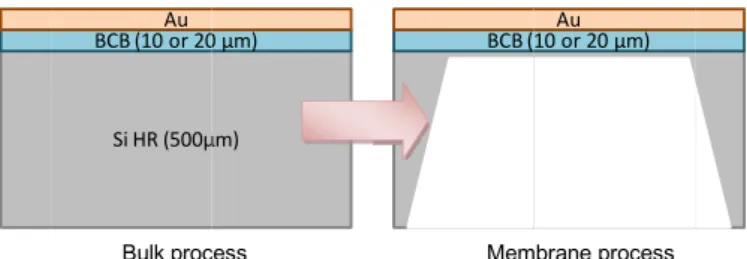
lobe level sta ceeds 0.5 time ations that the ications is ach 3.3 mm m go port 5 CPW monopole 20 363 µm ystem. licon to array mized n tool. lected same nd the nsions n the of the to the nance is the ations 5 mm gth in as are upling nd the upling s also ntenna mutual arts to es the e best hieved when of th low coup Th array depo µm t layer the etchi not v simu More found Th bridg to c poten wave Th switc The m the m phase the a MEM loss respe actua Th shifts mark ld 0 µm n the inter-ele he monopole i side lobe le pling remains s he BCB memb y is presented osited on the c thick electropl r. Finally the desired locat ing as it is sho vertical and ulations. The e detailed des d from [9]. he membrane ges using MEM connect groun ntials between elengths. he digital pha ched delay-lin membrane pro membrane bu e shifters can antenna array. MS switch are and return lo ectively. The ation voltage i he structure o s is presented ked by green b Si HR (500µ BCB (10 or 20Au Bulk proc Fig. 3. Membr ement spacing i.e. 1.90 mm. evel and, on sufficiently lo brane process in Fig. 3. Fir clean HR silic lating gold lay thick HR sili tions using P own in Fig. 3. this has to b angle of the scription of t e process allo MS technolog nd planes o n ground plan III. PHASE ase shifter ha ne technique ocess describe ut is also a M n be manufact The structure e presented in oss of the swi isolation of t is 43.8 V. of the phase d in Fig. 5. Th
boxes and lette
Fig. 4. Parallel M µm) 0 µm) cess rane process. equals to two The selected the other h ow.
used for desi st, a 20 µm th con substrate. yer is grown o con substrate Potassium H . The walls of be taken into e walls is ap the membrane ows also man gy. These air b f the CPWs nes at the inte
E SHIFTER
as been imple and parallel ed in Section I MEMS proces
tured with the e and dimensio Fig. 4. The si itch are 0.62 the switch is shifter with he locations of ers “SW”. The MEMS switch. BCB ( Mem
o times the len d value leads hand, the mu gning the ante hick BCB lay . After this, a on top of the B is removed f Hydroxide (KO f the substrate o account in pproximately e process can nufacturing of bridges were u s to compen ervals of a qua emented with MEMS switc II allows not o ss. Therefore, e same proces ons of the par imulated inser dB and 13.2 31.3 dB and 9 different ph f the switches e phase shift g Si HR 10 or 20 µm)Au mbrane process ngth to a utual enna er is a 1.8 BCB from OH) e are the 54º. n be f air used nsate arter h the ches. only the ss as rallel rtion dB, d the hase s are goes
from corr The belo shif refe des I the sep feed fed opti feed has des The it is pow the sen in t imp stru cha LENG Length 1 2 3 4 5 6 7 8 9 m -80° to +8 responds a pa e maximum s ow 2 dB. Th fter were op erred to maste cription of the In order to ver performance arately witho ding network in phase and ion would be ding network
only one laye ign which w e only option s very difficul wer dividers w Wilkinson di nsitive to refle the matching pact the perfo ucture of the aracteristic imp Fig. 5. Structure TA GTH OF THE PATHS Phase (°) -80 -60 -40 -20 0 20 40 60 80 80° by 20° st ath in the pha
imulated inse he dimension timized with er’s thesis of e phase shifter IV. FEEDIN
rify the simul e of the ante out the phase
was designed d with the sam
e to use Wil k. However, b er of metalliza would be need would be to u t to solder the will be used w ividers, but on ections from t g of the anten ormance of t feeding netw pedances of th
of the phase shift
ABLEI S IN THE PHASE SH Length in λ 7/9 λ 5/6 λ 8/9 λ 17/18 λ λ 19/18 λ 10/9 λ 7/6 λ 11/9 λ
teps and each ase shifter, as ertion loss of t ns of the swi HFSS. Inter Diane Titz [1 rs and the ME NG NETWORK lation results w enna array ha e shifters. Fo d so that all th me amplitude. lkinson powe because the m ation it does n ded for the W
use chip resis ese componen which are less
n the other ha the antenna a nna elements the feeding n work is presen he transmissio fter. HIFTERS. Path L2;L2’ L2;L1’ L2;L3’ L1;L2’ L1;L1’ L1;L3’ L3;L2’ L3;L1’ L3;L3’ h phase shift s given in Tab
the phase shif tch and the rested reader 10] for the de EMS switches with measurem as to be mea or this purpo he antennas c . The most re er dividers fo membrane pr not allow resis Wilkinson div stors but at 60 ts. Therefore,
lossy compar and, they are array. Any pro will conside network. The nted in Fig. 6 on lines which value ble 1. fter is phase rs are etailed . ments asured ose, a can be eliable or the rocess stance viders. 0 GHz basic red to more oblem erably basic 6. The h lead to eq ZC1’ impe of th simu inser coeff The p radia Th and t First, phase to de
A.
S Th is -20 to 64 3.2 d effici Fig p Ref lectio n co ef ficient [d B ] Fig. qual powers in = 112 Ω and edance values he feeding net ulation softwa rtion loss of ficient of -14 power losses o ation pattern m V. SIMULAT his section pr the radiation c , the radiatio e shift, and th emonstrate the Single antenna he reflection c 0.5 dB or sma 4 GHz. The m dBi at the ce iency is 90%. g. 7. Simulated re port 2 Z0 Z ZC2 Divider 1 t 56 -25 -22.5 -20 -17.5 -15 -12.5 -10 Ref lectio n co ef ficient [d B] 6. Feeding netwo n the antenna p d ZC2 = 50 Ω can be found twork was sim are. The feed9 dB for a dB across th of the feeding measurements. TION RESULTS resents the si characteristics on pattern has hen with differ e beam steerin a element coefficient of aller at the de maximum total nter frequenc eflection coefficie port 3 Z0 po Z ZC1 ZC2 o 2 por Z ZC1’ 58 Frequ S11 S22 S33 S44 S55 ork from 1 to 5 po ports are Z0 = Ω. Equations d e.g. from [1 mulated using ding network all the ports he 57-64 GHz g network are . OF THE ANTEN imulated scatt s of the design s been presen rent phase shi ng feature.
the monopole esired frequen
gain of the si cy and the sim
ents of the 5x1 lin rt 4 Z0 port 5 Z0 Divider 1 ZC1 Div rt 1 Z0 ZC2 60 62 uency [GHz] orts. 50 Ω, ZC1 = 5 for defining 11]. The struc g HFSS and A k has an ave and a reflec z frequency b acceptable for NNA ARRAY tering parame ned antenna ar nted without ift values in o e antenna elem ncy range from ingle monopo mulated radia
near antenna arra port 6 Z0 to 3 ZC2 ider 1 to 2 64 6 56 Ω, the cture ADS rage ction and. r the eters rray. any order ment m 57 ole is ation y. 6 66
Fig. 8. Simulated transmission coefficients between adjacent antenna elements.
(a)
(b)
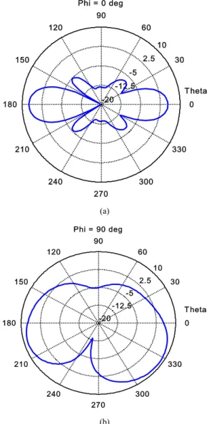
Fig. 9. Total gain patterns of the 5x1 antenna array in (a) the XZ-plane (phi = 0°) and (b) the YZ-plane (phi = 90°).
Fig. 10. Total gain patterns of the 5x1 antenna array in the XZ-plane (phi = 0°) with three different phase shift values.
B.
Antenna array with phase shiftersThe simulated reflection coefficient for each antenna element of the 5x1 linear antenna array are shown in Fig. 7. The matching is better than -13.5 dB at the desired frequency range. The minimum isolation between the adjacent antenna elements is 10.4 dB as shown in Fig 8. The isolation was tried to improve by adding wave traps between the antenna elements. However, adding the wave traps lead to worse matching and it was decided to leave them out from the design. The radiation pattern of the antenna array is presented in Fig. 9 when all the ports are fed in phase. Normally, the maximum radiation direction of the linear antenna array would be towards the Z-axis but the surrounding substrate material tilt the radiation pattern towards the Y-axis. Also this finding indicates how important it is to take into account the supporting substrate in the design process and simulations. The maximum total gain of the antenna array is 9.0 dBi and it is achieved when θ = 330° and φ = 90°. The coordinate system is presented in Fig. 1.
The radiation patterns of the antenna array with three different phase shift values are presented in Fig. 10 for the XZ-plane. The phase shifter enables a phase shift from -80° to +80° with 20° steps. The beam of the antenna array can be tilted ±30° and the maximum variation of the total gain level is less than 3 dB at this angle range.
VI. CONCLUSIONS
In this work a 5x1 linear antenna with phase shifters has been designed for 60 GHz beam steering applications. The antenna array has been designed using the membrane technology in order to achieve high radiation efficiency and good radiation characteristics. The matching of the antenna elements is better than -13.5 dB and the minimum isolation between the adjacent antenna elements is 10.4 dB at the desired frequency range from 57 to 64 GHz. The maximum total gain of the antenna array is 9.0 dBi and the radiation
56 58 60 62 64 66 -15 -14 -13 -12 -11 -10 -9 -8 Frequency [GHz] Transmission coe fficient [dB ] S21 S32 S43 S54 Phi = 0 deg 10 2.5 -5 -12.5 -20 0 30 60 90 120 150 180 210 240 270 300 330 T heta 10 2.5 -5 -12.5 -20 0 30 60 90 120 150 180 210 240 270 300 330 Phi = 90 deg T heta 10 2.5 -5 -12.5 -20 0 30 60 90 120 150 180 210 240 270 300 330 Phi = 0 deg 0 deg +80 deg -80 deg T heta
efficiency is 87 %. The phase shifters designed for the antenna array enable a phase shift from -80° to +80° with 20° steps. The beam steering feature was demonstrated by showing the radiation pattern of the antenna array with different phase shift values. The beam steering antenna array will be manufactured and the performance of the prototype will be verified with measurements in the future.
ACKNOWLEDGMENT
This work was supported by Academy of Finland through the CoE in Smart Radios and Wireless Research (SMARAD) and Tekes through BRAWE project.
REFERENCES
[1] A. J. Paulraj, D. A. Gore, R. U. Nabar, and H. Bölcskei, “An overview of MIMO communications—A key to gigabit wireless,” Proceedings
of the IEEE, vol. 92, no. 2, pp. 198–218, Feb. 2004.
[2] X. Guan, H. Hashemi, and A. Hajimiri, “A fully integrated 24-GHz eight-element phased-array receiver in silicon,” IEEE Journal of
Solid-State Circuits, vol. 39, no. 12, pp. 2311-2320, 2004.
[3] C.-H. Tseng, C.-J. Chen, and T.-H. Chu, “A low-cost 60-GHz switched-beam patch antenna array with butler matrix network,” IEEE
Antennas and Wireless Propagation Letters, vol. 7, pp. 432-435, 2008.
[4] S. Lee, S. Song, Y. Kim, J. Lee, C.-Y. Cheon, K.-S. Seo, and Y. Kwon, “A V-band beam-steering antenna on a thin-film substrate with a flip-chip interconnection,” IEEE Microwave and Wireless Components
Letters, vol. 18, no. 4, pp. 287-289, 2008.
[5] S. Lee, Jung-Mu Kim, Jong-Man Kim, Y.-K. Kim, C. Cheon, and Y. Kwon, “V-band single-platform beam steering transmitters using micromachining technology,” in Proc. IEEE Microwave Symposium
Digest, San Francisco, CA, USA, June 11-16, 2006, pp. 148-151.
[6] D. Neculoiu, G. Konstantinidis, L. Bary, A. Muller, D. Vasilache, A. Stavinidris, P. Pons, and R. Plana, “Membrane-supported Yagi-Uda mm-wave antennas,” in Proc. IEEE EuCAP 2006 European
Conference on Antennas and Propagation 2006, Nice, France, Nov.
6-10, 2006, CD-ROM (ISBN 978-92-9092-937-6), paper: session OA18, 350305.
[7] A. Muller, M. Saadaoui, P. Pons, D. Neculoiu, L. Bary, D. Dubuc, K. Grenier, D. Vasilache, C. Buiculescu, I. Petrini, and R. Plana, “Membrane supported endfire antennas manufactured using silicon micromachining,” in Proc. IEEE IWAT 2005 International Workshop
on Antenna Technology, Singapore, Mar. 7-9, 2005, pp. 113 – 116.
[8] D. Neculoiu, G. Konstantinidis, T. Vähä-Heikkilä, A. Muller, A. Stavinidris, M. Kantanen, D. Vasilache, Z. Chatzopoulos, and M. Dragoman, “GaAs membrane-supported 60 GHz receiver with double folded slot antennas,” in Proc. Asia Pacific Microwave Conference, Macau, China, Dec. 16-20, 2008, CD-ROM (ISBN 978-1-4244-2641-6), paper: A1-28.
[9] V. Puyal, D. Dragomirescu, C. Villeneuve, J. Ruan, P. Pons, and R. Plana, “Frequency scalable model for MEMS capacitive shunt switches at millimeter-wave frequencies,” IEEE Trans. on Microwave Theory
and Techniques, vol. 57, no. 11, pp. 2824-2833, Nov. 2009
[10] D. Titz, MM-wave MEMS switches and phase shifters for antenna
arrays, Master thesis, Sophia-Antipolis, France, Laboratoire
d’Electronique, Antennes et Télécommunications (LEAT) Centre National de la Recherche Scientifique, June 2009 , 84 p.
[11] D. M. Pozar, Microwave Engineering, John Wiley & Sons, Inc., 1998, 716 p.