HAL Id: hal-00533120
https://hal.archives-ouvertes.fr/hal-00533120
Submitted on 21 May 2021
HAL is a multi-disciplinary open access
archive for the deposit and dissemination of
sci-entific research documents, whether they are
pub-lished or not. The documents may come from
teaching and research institutions in France or
abroad, or from public or private research centers.
L’archive ouverte pluridisciplinaire HAL, est
destinée au dépôt et à la diffusion de documents
scientifiques de niveau recherche, publiés ou non,
émanant des établissements d’enseignement et de
recherche français ou étrangers, des laboratoires
publics ou privés.
A high efficiency superconducting nanowire single
electron detector
Michael Rosticher, F.-R. Ladan, J.-P. Maneval, S.N. Dorenbos, T. Zijlstra, T.
M. Klapwijk, V. Zwiller, Adrian Lupascu, Gilles Nogues
To cite this version:
Michael Rosticher, F.-R. Ladan, J.-P. Maneval, S.N. Dorenbos, T. Zijlstra, et al.. A high efficiency
superconducting nanowire single electron detector. Applied Physics Letters, American Institute of
Physics, 2010, 97 (18), pp.183106. �10.1063/1.3506692�. �hal-00533120�
Appl. Phys. Lett. 97, 183106 (2010); https://doi.org/10.1063/1.3506692 97, 183106 © 2010 American Institute of Physics.
A high efficiency superconducting
nanowire single electron detector
Cite as: Appl. Phys. Lett. 97, 183106 (2010); https://doi.org/10.1063/1.3506692
Submitted: 11 July 2010 . Accepted: 05 October 2010 . Published Online: 03 November 2010
M. Rosticher, F. R. Ladan, J. P. Maneval, S. N. Dorenbos, T. Zijlstra, T. M. Klapwijk, V. Zwiller, A. Lupaşcu, and G. Nogues
ARTICLES YOU MAY BE INTERESTED IN
Picosecond superconducting single-photon optical detector
Applied Physics Letters 79, 705 (2001); https://doi.org/10.1063/1.1388868 Efficient single particle detection with a superconducting nanowire AIP Advances 2, 032124 (2012); https://doi.org/10.1063/1.4740074
Single-photon detectors combining high efficiency, high detection rates, and ultra-high timing resolution
A high efficiency superconducting nanowire single electron detector
M. Rosticher,1F. R. Ladan,1J. P. Maneval,1S. N. Dorenbos,2,a兲T. Zijlstra,2T. M. Klapwijk,2 V. Zwiller,2A. Lupaşcu,3,4and G. Nogues3,5
1
Laboratoire Pierre Aigrain, CNRS, ENS, UPMC, 24 rue Lhomond, 75231 Paris Cedex 05, France 2
Kavli Institute of Nanoscience, Delft University of Technology, 2628CJ Delft, The Netherlands 3
Laboratoire Kastler Brossel, CNRS, ENS, UPMC, 24 rue Lhomond, 75231 Paris Cedex 05, France 4
Institute for Quantum Computing, University of Waterloo, 200 University Av. W, Waterloo, Ontario N2L 3G1, Canada
5
Institut Néel/CNRS, Université Joseph Fourier, CEA-BP 166, 38042 Grenoble, France
共Received 11 July 2010; accepted 5 October 2010; published online 3 November 2010兲
We report the detection of single electrons using a Nb0.7Ti0.3N superconducting wire deposited on
an oxidized silicon substrate. While it is known that this device is sensitive to single photons, we show that it also detects single electrons with kilo-electron-volt energy emitted from the cathode of a scanning electron microscope with an efficiency approaching unity. The electron and photon detection efficiency map of the same device are in good agreement. We also observe detection events outside the active area of the device, which we attribute to sensitivity to backscattered electrons. © 2010 American Institute of Physics. 关doi:10.1063/1.3506692兴
The versatility of superconducting nanowires as single particle detectors relies on their sensitivity to the minute amount of energy required to locally induce a resistive tran-sition. From this point of view, the latest achievements in-volving the detection of organic molecules1and photons in the infrared range2 all derive from early experiments with
␣-particles in the million electron volt range.3In order to go beyond the optical resolution limit, the scanning electron mi-croscope共SEM兲 working at low temperature,4proved useful. This technique enabled the visualization of the real size of the hot spot caused by a detection process.5 However, the best achieved spatial resolution is limited by thermal diffu-sion to about 1 m and single electron detection has not been demonstrated. In this paper, we show single electron detection using a superconducting nanowire. Our supercon-ducting single electron detector共SSED兲 offers a high spatial and timing resolution and we compare the electron detection efficiency map with a photon detection efficiency map, mea-sured on the same device.
The fabrication process of our superconducting nanowire has been described before.6 It consists of a 100 nm wide, 500 m long, and 6 nm thick wire of Nb0.7Ti0.3N. The wire is folded into an 10⫻10 m2 area, with a separation of 100 nm between adjacent detecting branches. One end of the wire is grounded whereas the other end is connected to a cryogenic coaxial cable used to inject a current through the structure. We measure a dc critical current Ic= 10 A at
4.2 K and Ic= 5.2 A at 8 K. Our experimental setup
con-sists of a cryogenic SEM.7The detector is mounted on a cold translation stage at T = 8 K under the electronic beam of an SEM. The SEM current Ibis controlled and can be measured
with a picoammeter共measurement uncertainty 10%兲. The en-ergy of the incident electrons Eecan be varied between 5 and
30 keV.
To block low frequency 1/ f noise we use a dc-block, through which we can only bias the wire with pulses of cur-rent amplitude I and duration td= 800 ns共see inset of Fig.1兲.
Each pulse is reflected by the circuit. When the current is on,
the detection of an electron triggers a short pulse at the out-put of the system 共duration of a few nanoseconds, see inset of Fig. 1兲. The change in baseline is caused by the limited
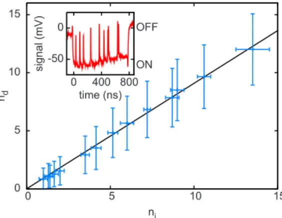
bandwidth 共0.1 to 1000 MHz兲 of the amplification of the output pulses but does not affect the bias current of the SSED. We count the average number of detection pulses and compare it to the average incoming number of electrons ni
= Ib⫻td/e in order to infer the absolute detection efficiency . We can adjust the current Ib down to a few picoamperes,
and obtain single electrons separated by approximately 100 ns. We have measured the number of detection events nd
versus incoming electrons ni 共Fig. 1兲. The linearity of this
plot shows that we detect single electrons. A complete map of is obtained by scanning the electron beam over the sample with a full control of the step size and dwell time.
To compare the relative performances of our supercon-ducting nanowire detector for single electrons and single photons, we present in Fig.2共a兲a two-dimensional共2D兲 plot of the photon detection efficiency for our sample, obtained by scanning a laser spot 共1 m diameter兲 over the detector with an intensity, low enough to be in the single photon
a兲Electronic mail: [email protected].
-50 0 0 400 800 signal (mV) time (ns) OFF ON 0 5 10 15 0 5 10 15 nd ni
FIG. 1. 共Color online兲 Average number of counted peaks per bias current pulse nd as a function of the number of incoming electrons ni= Ib⫻td/e 共Ee= 10 keV, I/Ic= 0.85兲. A linear fit 共solid line兲 gives a detection efficiency
= 0.91共0.01兲. 共Inset兲 A typical experimental signal at the output of the detection chain. One pulse corresponds to the detection of one electron.
APPLIED PHYSICS LETTERS 97, 183106共2010兲
regime. A detailed description of the setup is given in Ref.8. The map shows spatial variations over the active area that could originate from structural and/or chemical inhomogene-ities of the layer. This reference image can be compared to Fig.2共b兲which shows the detection efficiency for electrons of energy 30 keV and a detector bias current I/Ic= 0.35. We
observe that the electron detection efficiency is more homo-geneous than in the case of photon detection. There exists however a clear correlation between the two measurements, with the maxima and minima located at the same positions for both images. It demonstrates that the detection process is affected in the same way for both particles. It shows also that SEM measurements could be used to characterize the performances of superconducting nanowires for photon de-tection. With increasing bias current, the electron detection efficiency saturates and becomes homogeneous over the whole detector active area as illustrated by Fig. 2共c兲 共I/Ic
= 0.85, Ee= 20 keV兲. We note that we have also been able to
produce electron detection efficiency maps with NbN wires of 500 and 1000 nm widths.7 However, the present NbTiN detector covers a larger area and offers a better efficiency with fewer inhomogeneities.
In both Figs.2共b兲and2共c兲, one observes sharper details than in Fig.2共a兲. This is expected as electron microscopy has a much better spatial resolution than optical microscopy. In order to evaluate our spatial resolution, we present in Fig.
2共d兲a 1⫻1 m2image of the detection efficiency taken in
the conditions of Fig.2共c兲. The plot directions make an angle of 60° with respect to the wire direction. It reveals the inner structure of the detector via a small modulation of the detec-tion efficiency 共0.05 modulation, compared to an average efficiency of 0.85兲. The period of the modulation corre-sponds to the pitch of the meander structure and the visibility of this modulation indicates a spatial resolution of less than 100 nm. We also observed that for electron energies Ee
ⱕ10 keV, the spatial resolution is degraded 共to about 850 nm full width at half maximum兲 and one can no longer
dis-tinguish individual wires. We attribute this loss of perfor-mance to charging effects on the substrate which degrade the SEM spatial resolution.
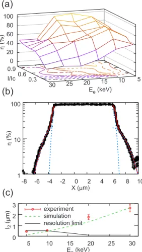
Figure3共a兲summarizes our results foras a function of
I/Ic and Ee. It shows that increases with increasing I/Ic
and decreases with increasing electron energy. This fact is in good agreement with previous studies that showed that the mean electron energy loss⌬Eeis of the order or 100 eV for
the impinging electron energy range we have explored.9 Moreover, one has ⌬Ee= S⫻in, where in is the inelastic
mean free path of the electron and S is the stopping power of the material, which is well described by the Bethe formula10 or empirical variations of the latter.9,11To a first approxima-tion S = f共Ee兲/Ee and in= g共Ee兲⫻Ee where f and g are
slowly varying functions. As a consequence, the first inelas-tic collision in the detector happens deeper for high energy electrons and is less likely to trigger a transition of the nano-wire, explaining the decrease in with increasing Ee. The
low efficiency at Ee= 5 keV共60%兲 is not consistent with this
model. Our hypothesis is that it arises from trapped charges in the vicinity of the detector共i.e., in a dielectric or noncon-ductive material兲 close to the SSED that are also responsible for the degradation of the spatial resolution of the 2D-plots at this energy.
(a)
-5 0 5 x (μm) -5 0 5 0 1 2 3 η (%)(b)
-5 0 5 x (μm) -5 0 5 y( μm) 0 5 10 15 20 25 η (%)(c)
-5 0 5 x (μm) -5 0 5 0 20 40 60 80 η (%)(d)
0 0.3 0.6 0.9 x' (μm) 0 0.3 0.6 0.9 y' (μ m) 80 82 84 86 88 90 η (%)FIG. 2. 共Color online兲 2D plots of the detection efficiency. 共a兲, for single photons共=532 nm, I/Ic= 0.8, step size⬃100 nm兲. The white area corre-sponds to missing data 共b兲, for single electrons 共bias current I/Ic= 0.35, electron energy Ee= 30 keV, SEM step size 200 nm兲. 共c兲, same map as 共b兲 with I/Ic= 0.85, Ee= 20 keV and SEM step size 200 nm.共d兲 Zoom of 共c兲 for a 1⫻1 m2area, with SEM step size of 20 nm. A square shown in共c兲 indicates the relative scale and orientation of共d兲.
(a)
0.3 0.6 0.9 I/Ic 30 25 20 15 10 5 Ee(keV) 0 20 40 60 80 100 η (%) 1 10 100 -8 -6 -4 -2 0 2 4 6 8 10 η (%) X (μm)(b)
0 1 2 3 5 10 15 20 25 30 l2 (μ m) Ee(keV)(c)
experiment simulation resolution limitFIG. 3. 共Color online兲 共a兲 Electron detection efficiency for different values of bias current and electron energy. The beam position is fixed and close to the center of the active area. 共b兲 Cross-section of the detection efficiency map of Fig.2共c兲共log scale兲. The fall in detectivity at the edge of the active area is fitted by a double Gaussian共dotted lines: individual Gaussians, solid line: sum兲 with characteristic lengths l1= 330 nm and l2= 1760 nm, respec-tively.共c兲 Plot of l2as a function of the electron energy Ee. At high energy 共ⱖ10 kV兲, it is in good agreement with Monte Carlo simulations of the mean radius of exit for backscattered electrons, done in Ref.12.
Evidence of the detection of backscattered electrons is provided by the cross-section of the efficiency map of Fig.
2共c兲, presented in Fig. 3共b兲. We observe shoulders for the detection efficiency signal at the detector edges, proving that it is still possible to detect electrons impinging at distances larger than the SEM spatial resolution. A double Gaussian fit at the edge for different cross-sections, both horizontal and vertical, gives two average characteristic lengths l1
= 330共40兲 nm and l2= 1760共230兲 nm, with a ratio in ampli-tude around 80:20. We attribute the first length to the finite step size of the SEM beam for this experiment. We attribute the second length scale to the detection of backscattered electrons. This distance is consistent with Monte Carlo simu-lations of the electron trajectories that predict a mean dis-tance between the entry and exit points of lMC= 1320 nm.
This distance depends strongly on the energy of the incident electron. We present in Fig.3共c兲a comparison of l2and lMC
for different values of Ee. At low energy, the distance lMC is
of the order of or lower than the apparatus spatial resolution degraded to 500 nm. We only observe a single Gaussian. At larger energies, above 10 keV, the agreement between ex-periment and simulation is very good.12
In conclusion, we have operated a fast and efficient single electron counter using a superconducting nanowire. We show an efficiency close to unity. Its low noise, short dead time, and high timing accuracy make this device inter-esting in situations where a cryogenic environment is avail-able. Optimizing further these devices for the specific pur-pose of electron detection can certainly improve future performances. For example, a thin conducting layer on top of the nanowire can reduce the charging effect and improve the efficiency for low energy electrons共ⱕ5 keV兲. For high en-ergy electrons, increasing the superconducting layer thick-ness will improve the performances. Fabricating the devices over a thin membrane would avoid backscattering. Arrays of such devices, could provide an imaging system for electrons with a time resolution below 60 ps13and a pixel size below 10 m. Those figures could significantly improve the
tech-nologies presently used for example in ultrafast electron microscopy.14
M.R., F.R.L., J.P.M., A.L., and G.N. thank the Japan Science and Technology Corporation 共ICORP: “Quantum Entanglement”兲 and the Région Ile de France 共Cnano IdF project兲. A.L. acknowledges support from the European Union through a Marie Curie fellowship. S.D. and V.Z. ac-knowledge NWO for funding. We thank Reinier Heeres for help with the optical measurement. T.M.K. acknowledges NWO for funding through Grant No. 614.061.010.
1N. Zen, A. Casaburi, S. Shiki, K. Suzuki, M. Ejrnaes, R. Cristiano, and M. Ohkubo,Appl. Phys. Lett. 95, 172508共2009兲.
2G. Gol’tsman, O. Minaeva, A. Korneev, M. Tarkhov, I. Rubtsova, A. Divochiy, I. Milostnaya, G. Chulkova, N. Kaurova, B. Voronov, D. Pan, J. Kitaygorsky, A. Cross, A. Pearlman, I. Komissarov, W. Slysz, M. Wegrzecki, P. Grabiec, and R. Sobolewski,IEEE Trans. Appl. Supercond.
17, 246共2007兲.
3D. E. Spiel, R. W. Boom, and J. E. C. Crittenden,Appl. Phys. Lett.7, 292 共1965兲.
4J. R. Clem and R. P. Huebener,J. Appl. Phys. 51, 2764共1980兲. 5R. Gross and D. Koelle,Rep. Prog. Phys. 57, 651共1994兲.
6S. N. Dorenbos, E. M. Reiger, U. Perinetti, V. Zwiller, T. Zijlstra, and T. M. Klapwijk,Appl. Phys. Lett. 93, 131101共2008兲.
7A. Lupascu, A. Emmert, M. Brune, G. Nogues, M. Rosticher, J. P. Maneval, F. R. Ladan, and J. C. Villegier, Proceedings of the 2009 IEEE Toronto International Conference on Science and Technology for Human-ity共TIC-STH兲, 2009, p. 1011. doi:10.1109/TIC-STH.2009.5444534 8S. N. Dorenbos, E. M. Reiger, N. Akopian, U. Perinetti, V. Zwiller, T.
Zijlstra, and T. M. Klapwijk,Appl. Phys. Lett. 93, 161102共2008兲. 9A. Jablonski, S. Tanuma, and C. J. Powell,Surf. Interface Anal. 38, 76
共2006兲.
10H. Bethe and J. Ashkin, Experimental Nuclear Physics共Wiley, New-York, 1953兲.
11D. C. Joy and S. Luo, Scanning 11, 176共1989兲.
12D. Drouin, A. R. Couture, D. Joly, X. Tastet, V. Aimez, and R. Gauvin, Scanning 29, 92共2007兲.
13M. G. Tanner, C. M. Natarajan, V. K. Pottapenjara, J. A. O’Connor, R. J. Warburton, R. H. Hadfield, B. Baek, S. Nam, S. N. Dorenbos, E. Bermu-dez Urena, T. Zijlstra, T. M. Klapwijk, and V. Zwiller,Appl. Phys. Lett.
96, 221109共2010兲.
14W. E. King, G. H. Campbell, A. Frank, B. Reed, J. F. Schmerge, B. J. Siwick, B. C. Stuart, and P. M. Weber,J. Appl. Phys. 97, 111101共2005兲.