HAL Id: hal-02698862
https://hal.archives-ouvertes.fr/hal-02698862
Submitted on 5 Jan 2021HAL is a multi-disciplinary open access archive for the deposit and dissemination of sci-entific research documents, whether they are pub-lished or not. The documents may come from teaching and research institutions in France or abroad, or from public or private research centers.
L’archive ouverte pluridisciplinaire HAL, est destinée au dépôt et à la diffusion de documents scientifiques de niveau recherche, publiés ou non, émanant des établissements d’enseignement et de recherche français ou étrangers, des laboratoires publics ou privés.
Films
Larysa Khomenkova, K Makasheva, Peter Petrik, Caroline Bonafos, Nicolas
Ratel-Ramond, Oleksandr Melnichuk, Lyudmyla Melnichuk, I. Balberg,
Fabrice Gourbilleau, N. Korsunska
To cite this version:
Larysa Khomenkova, K Makasheva, Peter Petrik, Caroline Bonafos, Nicolas Ratel-Ramond, et al.. Thermally Stimulated Evolution of Optical and Structural Properties of Germanium-Doped Alumina Films. ECS Transactions, Electrochemical Society, Inc., 2020, 97 (2), pp.81-90. �10.1149/09702.0081ecst�. �hal-02698862�
Thermally Stimulated Evolution of Optical and Structural Properties of Germanium-Doped Alumina Films
L. Khomenkovaa,b, K. Makashevac, P. Petrikd, C. Bonafose, N. Ratel-Ramonde, O. Melnichukf, L. Melnichukf, I. Balbergg, F. Gourbilleauh, and N. Korsunskaa
a
V. Lashkaryov Institute of Semiconductor Physics, 45 Pr. Nauky, Kyiv 03028, Ukraine
b
National university “Kyiv-Mohyla academy”, 2 Skovorody str., Kyiv 04070, Ukraine
c
LAPLACE, Université de Toulouse, CNRS, UPS, INPT, 118 route de Narbonne, 31062 Toulouse, France
d
Institute for Technical Physics and Materials Science, Center for Energy Research, Konkoly Thege Rd. 29-33, 1121 Budapest, Hungary
e
CEMES/CNRS, 29 rue Jeanne Marvig, 31055 Toulouse Cedex 4, France
g
Mycola Gogol Nizhyn State University, 2 Grafska str, Nizhyn 16600, Ukraine
f
Racah Institute of Physics, Hebrew University, Givat Ram, Jerusalem, Israel
h
CIMAP, Normandie Univ, ENSICAEN, UNICAEN, CEA, CNRS, 6 Boulevard Maréchal Juin, 14050 Caen Cedex 4, France
Ge-doped Al2O3 films were deposited on long, non-rotated quarts
substrate by magnetron co-sputtering of Ge and Al2O3 space-apart
targets. This approach allowed to vary Ge content along the film length in the range 5-85 at.%. Simultaneous annealing treatment of such long samples permitted to investigate the evolution of optical and structural properties of the films with different Ge content. It was observed that all as-deposited films and those annealed at TA=550 °C during 50 min in nitrogen atmosphere were amorphous
whatever Ge content. The formation of Ge nanocrystals was observed after treatment at TA=600 °C during 1-15 min. The
higher Ge content, the shorter annealing time was required to form Ge nanocrystals. This annealing stimulated also an appearance of photoluminescence in visible-near infrared spectral range. Three specific bands centered at about 580-600 nm, 620-630 nm and 700-730 nm were detected. Their relative contribution was depended on Ge content determining the shape and peak position of luminescence spectrum. Two former components were ascribed to the carrier recombination via the defects in Ge oxide shell covered Ge nanocrystals, whereas the latter one was assumed to originate from carrier recombination in amorphous Ge clusters or via defects at Ge-cluster/Al2O3 interface. This statement was
supported by the heat treatment of the films at TA=700-800 °C
caused significant decrease of Ge content due to Ge out-diffusion from film volume via formation of volatile GeO.
Introduction
In recent decades, significant attention of research groups has been focused on silicon or germanium nanostructured materials. Since the first report on nanostructured Si-based
10.1149/09702.0081ecst ©The Electrochemical Society ECS Transactions, 97 (2) 81-90 (2020)
materials (1,2), optical and structural properties of free standing silicon nanocrystallites (Si-ncs) or those embedded in dielectric hosts were widely studied (3-10). A lot of efforts were concentrated on the development of different technological approaches for fabrication of Si-ncs, monitoring their size distribution and surface chemistry. An optical gain and electroluminescent emission were achieved offering the perspective to create all-in-one-chip Si-based optoelectronic devices. Significant knowledge on the light emission processes of Si nanostructured materials was obtained. The mechanisms of Si-ncs formation in different hosts were proposed.
It is interesting that size-dependent optical properties of germanium nanocrystals (Ge-ncs) were reported by Hayashi et al. much earlier than those of Si-ncs (11). Although the Ge-ncs were also studied by different research groups (see, for instance, 12-22), the corresponding publications were not so numerous unlike those on the Si-ncs embedded in different hosts. Recently, the attention of the researchers has been particularly renewed towards the Ge-ncs since they are environmentally friendlier alternatives to classical compound semiconductor nanocrystals being nontoxic, biocompatible, electrochemically stable and compatible with current microelectronics. The investigation of either free-standing Ge-ncs or those embedded in dielectric hosts was reported (23-28).
As compared to silicon, germanium is especially appealing due to the larger dielectric constant, higher electron and hole mobility, smaller effective masses of electrons and holes. A narrower bulk band gap (0.66 eV for Ge against 1.1 eV for Si) and a larger absorption coefficient offered a possibility for tuning of light emission in wider spectra range. Bohr exciton radius of germanium, rBGe=24.3 nm, is significantly larger than that
of silicon (rBSi=4.5 nm) (12). This means that Ge-ncs will impart stronger, more easily
identified quantum confinement effects than Si-ncs with the same sizes. Moreover, quantum confinement effects will emerge for larger Ge-ncs than that for Si-ncs (25). Due to this property, the Ge-ncs are considered to be ideal nodes for memory devices (17,21,23,26). Being crystallized at lower temperature and offering a negative conduction band offset with respect to the Si substrate, the Ge-ncs provide a larger memory window than devices based on Si-ncs with improved retention time (16,21).
The Ge-ncs embedded in SiO2 host were mainly studied. However, Al2O3 is an
interesting material not only for microelectronic application, but also for optical communication due to its relatively higher refractive index (1.73 at 1.95 eV) in comparison with that of SiO2 (1.46 at 1.95 eV) offering better light confinement.
Although Al2O3 waveguides doped with Si or Ge and rare-earth ions were developed for
optical communications (28,31), such materials are still less addressed. The present paper reports the fabrication of Ge-doped Al2O3 films with different Ge content by magnetron
co-sputtering and the effect of post-deposition processing on the structural and optical properties of these materials.
Experimental details
Ge-rich Al2O3 films were deposited on long non-rotated quarts substrates by
radio-frequency magnetron sputtering of two spatially separated targets, pure Ge and pure Al2O3. The diameter of each target was 2 inches. The length of quartz substrate was 15
performed in an argon atmosphere at a pressure of 1.1 Pa for 250 minutes. The power densities applied to Al2O3 and Ge targets were 0.98 and 0.49 W/cm2, respectively. The
substrate temperature was 15 °C. Using this deposition approach, the films with variation of Ge content along the film length were obtained. Besides, pure Ge and pure Al2O3 films
were also produced by the sputtering of corresponding target only at the same conditions. More details about this approach can be found in (27). To form Ge-ncs, the heat treatment of the films was performed in conventional horizontal furnace at TA
=500-800 °C during 1-50 min in nitrogen atmosphere.
Optical and structural properties of the films were studied by spectroscopic ellipsometry, Raman scattering, X-ray diffraction (XRD) and photoluminescence (PL) methods. Spectroscopic ellipsometry measurement was performed by means of a Jobin-Yvon ellipsometer (UVISEL, HORIBA Ltd., Kyoto, Japan), where the incident light was scanned in the range of 1.5 to 4.5 eV under an incident angle of 66.3°. The fitting of the experimental data was performed using DeltaPsi2 software (HORIBA Ltd., Kyoto, Japan). The refractive indexes are reported being taken at 1.95 eV. Raman scattering and photoluminescence spectra were recorded with a double grating monochromator equipped with CCD camera. Solid-state laser with the 532-nm wavelength was used as excitation source. The power density of this excitation light was chosen to prevent any heating of the films during spectrum recording. XRD data were collected in a 2θ range of 20°-80° with Cu Kα radiation (0.1514 nm) of a Philips X'PERT HPD Pro device. An
asymmetric grazing geometry (ω~0.5°) was chosen to increase the volume of material interacting with the X-ray beam. The data were compared with standard cards of Powder Diffraction File Database (#4-0545 for cubic Ge). All measurements were performed at room temperature. The combination of these non-destructive methods allows information about microstructural and optical properties of the films to be obtained.
Results and discussion
Spectroscopic ellipsometry
Being a fast, sensitive, and non-destructive method, spectroscopic ellipsometry is used for the determination of the thickness of thin film and its optical parameters (such as refractive index, n, and absorption coefficient,
α
). The fitting of experimental data obtained for Ge-Al2O3 films as well as pure Ge and pure Al2O3 counterparts wasperformed using the approach described in (4,7). For pure Ge and pure Al2O3 films the
refractive indexes (taken at 1.95 eV) were estimated as nGe=4.21±0.01 and nAl2O3=1.75±0.01, respectively. The fitting of the spectra of Gex(Al2O3)1-x film deposited
on long substrate revealed the variation of the refractive index (taken at 1.95 eV) from
n=1.81±0.01 (Al2O3-rich side) up to n=3.85±0.01 (Ge-rich side) along the film length.
The thickness of the films was varied from 450±5 nm (Al2O3-rich side) up 1300±10 nm
(Ge-rich side). This thickness variation was caused by the higher sputtering yield of Ge target in comparison with that of Al2O3 one.
Earlier, we have shown that for composite Si-rich Al2O3 and Si-rich HfO2 thin films
grown by magnetron sputtering, the use of the effective medium approximation permits to determine the relationship between the refractive index n and film stoichiometry x (4,7,30,31). The same procedure was applied in present study for Ge-rich Al2O3 films.
Since the experimental spectra were featureless, this allowed assuming that the films are
amorphous and can be considered as an effective medium which dielectric constant is determined by the relative contribution of Ge and Al2O3 components as
2 3 2 3 Al O Ge Ge Al O
(1
)
0
2
2
eff eff eff effx
x
ε
− ε
ε
− ε
+
−
=
ε
+
ε
ε
+
ε
[1]where εeff is the dielectric permittivity of composite material, εGe and εAl2O3 are the
dielectric permittivity of Ge and Al2O3, respectively, and x is the fraction of the Ge
component. Thus, our Ge-rich films can be considered as Gex(Al2O3)1-x medium. Taking
into account the n values obtained by the fitting of experimental ellipsometry spectra, the
x values of Gex(Al2O3)1-x films were found to vary from x=0.05 (at Al2O3-rich side) up to x=0.85 (at Ge-rich side). It should be noted that the films with х>0.7 can be considered
rather as a Ge film enriched with Al2O3, than Al2O3 host doped with Ge.
Raman scattering spectra
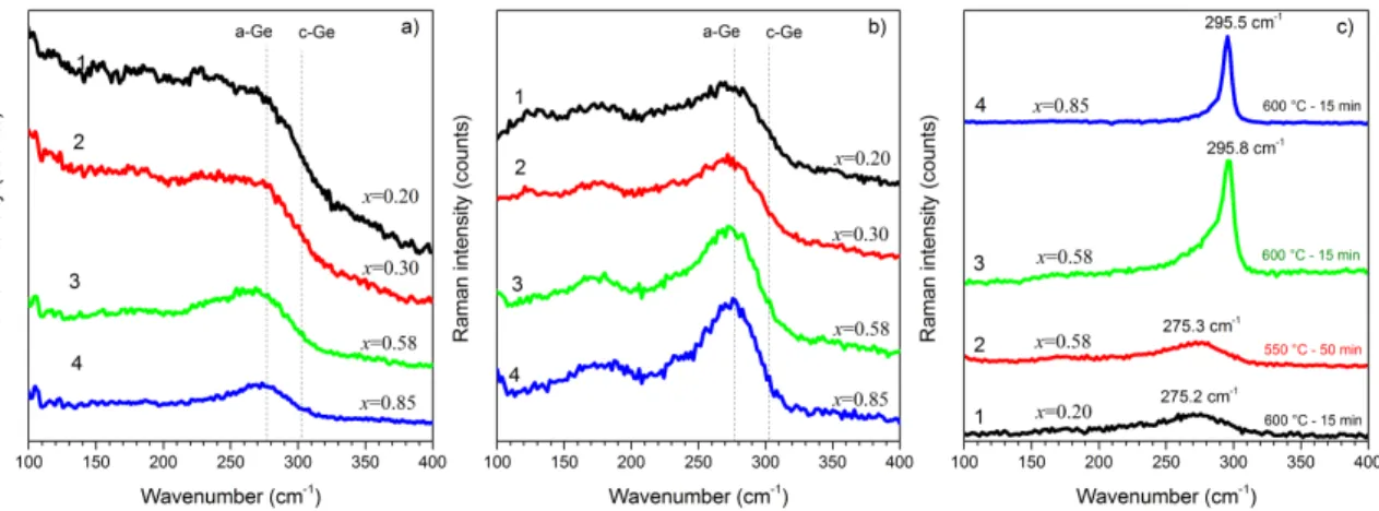
As-deposited Gex(Al2O3)1-x films were found to be amorphous. For the films with x>0.6,
the peak position of Ge TO phonon was found at ωTO≈270-274 cm-1 (Fig.1,a). This
spectral position is similar to that observed in amorphous germanium. When Ge content decreases to x=0.1, the broadening of Raman scattering spectrum and shift of the ωTO
down to 268 cm-1 were observed. This shift is the evidence that the structure of the films was unrelaxed. This can be caused by the presence of point defects as well as by the tensile stress appeared due to mismatching between the lattice parameters of Ge (a=0.566 nm) and Al2O3 (a=0.792 nm for cubic; a=0.475 nm, c=1.299 nm for hexagonal alumina
(32)). It should be noted that Raman scattering spectra for the films with x<0.1 were not recorded due to high transparency of the films. Significant contribution of amorphous Ge phase in the films with x≥0.2 (Fig.1,a) testifies to the formation of Ge amorphous inclusions during deposition process similar to the effect reported for Si-rich Al2O3 films
(4,7,10,27).
Figure 1. Raman scattering spectra of as-deposited samples (a) and those annealed at TA=550 °C for 50 min (b) and 600 °C for 15 min (c). The Ge content is mentioned in the
figures. The spectra are vertically shifted for clarity. The vertical dashed lines show the peak position of Raman signal for amorphous (a-Ge) and bulk (c-Ge) germanium.
The heat treatment of the films at TA=500 °C did not affect film structure. Whatever
annealing time, all these films kept amorphous nature. The TA rise up to 550°C led to the
increase of the intensity of Raman signal and its narrowing accompanied by the shift of peak position towards higher wavenumbers (ωTO≈272-275 cm-1) that is the evidence of
the stress relaxation. This transformation of Raman spectra was more pronounced for the films with x<0.6 (Fig. 1,b). The longer annealing time enhanced this effect. It should be noted that these annealed films became more transparent that can be caused by the formation of Ge clusters as well as appearance of GeO2 due to phase separation process.
It is worth to point out that the formation of volatile GeO can be ruled out for this annealing temperature.
Annealing of the films at TA=600 °C resulted in further narrowing of Raman signal
and its shift towards ωTO≈275 cm-1 for x<0.6 (Fig.1,c). However, this final peak position
showed that whatever annealing time, the Ge inclusions are rather amorphous than nanocrystalline. This result demonstrates that in the contrast to the ability of aluminum to enhance Ge crystallization (33), in our films with x<0.6 and annealed at TA=600 °C
amorphous Ge phase is stable. This result was similar to those reported in (34) for Ge-Al2O3/Al2O3 superlattices. At the same time the shift of peak position to higher
wavenumbers than that of amorphous Ge is the evidence of full relaxation of tensile stresses and, even, an appearance of compressive ones that can be caused by the transformation of Al2O3 host as well as by underlying quarts substrate.
In the films with x>0.6, the Raman peak showed its narrowing and shift towards ωTO≈295 cm-1 (Fig.1,c) that is the evidence of the crystallization of Ge clusters. It should be noted that the higher Ge content, the more pronounced Ge crystallization takes place and the shorter time is required for Ge-ncs formation. Further increase of TA up to
700-800 °C caused not only Ge-ncs formation, but also the decrease of Raman signal intensity (not shown here). This phenomenon was explained by the Ge out-diffusion from the films via formation of volatile GeO. The results described above were supported by XRD data. XRD data
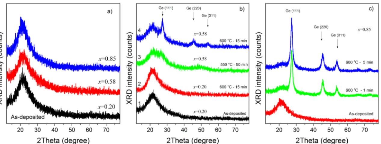
Figure 2,a shows the XRD patterns of as-deposited films with different Ge content. All films demonstrate abroad scattering peak indicating its amorphous nature. Similar XRD patterns were recorded for the films with x<0.5 annealed at TA=550 and 600 °C
(Fig.2,b) At the same time, for the films with x>0.5, the appearance of the features at 2θ=27.23° and 50.0° as well as their enhancement after film annealing at 600 °C was observed testifying to the formation of Ge inclusions via phase separation. This result is in agreement with Raman scattering data. As one can see from Fig.2, the higher Ge content, the shorter time is required for the formation of Ge crystallites.
Three peaks marked as (111), (220) and (311) in Fig.2b,c are the signature of Ge-ncs formation that are randomly oriented. However, corresponding peak positions are observed at 2θ=27.23, 45.36 and 53.70° for x=0.58 (Fig.2,b) and 2θ=27.32, 45.49 and 53.80° for x=0.85 (Fig.2,c) being shifted in comparison with those reported for Ge standard (2θ=27.28, 45.30 and 53.68°). This indicates in the presence of residual compressive stress in the films with x=0.85. This finding is in agreement with the data that obtained from Raman scattering method (Fig.1,c).
Figure 2. XRD patterns as-deposited (a) and annealed (b,c) films. Annealing parameters and Ge content in the films are mentioned in the figures. The patterns are vertically shifted for clarity.
The estimation of coherent domain sizes, d, using Scherrer formula revealed that in the films with x=0.58 annealed at TA=600 °C during 15 min d=3.8-4.0 nm. At the same time,
for the film with x=0.85 annealed at TA=600 °C during 1 min d=4.9-5.0 nm. Longer
annealing time (5 min) resulted in the d increase up to 8.0-8.2 nm. The analysis of the intensities of XRD peaks showed that the Ge-ncs in these films may have elongated shape with large size in (111) direction.
The comparison of XRD and Raman scattering data revealed the discrepancy between Ge-ncs sizes and corresponding Raman peak positions. This is an additional confirmation of the presence of residual stress in Ge-doped Al2O3 films that brings some difficulty in
the estimation of Ge-ncs sizes from Raman scattering spectra. Similar effects have been reported for Ge-doped HfO2 and Si-doped Al2O3 films by different groups (7,8,18,27). To
determine real sizes of Si or Ge crystallites embedded in these hosts, the investigation of such films with transmission electron microscopy was performed. These studies for our Ge-doped Al2O3 films are in progress.
Photoluminescence
Photoluminescence (PL) study of as-deposited films revealed a weak PL emission only for the samples with low Ge content (x<0.2). It is peak position was observed at 560-570 nm and this band was found to be similar to the PL band reported in (4,7,35) for the F2+ centers in Al2O3 host. The heat treatment at TA=500-550 °C did not changed the
PL spectra of the films (whatever annealing time and Ge content). Further TA increase up
to 600 °C caused an appearance of three PL bands peaked at 580-600 nm, 620-630 nm and 700-730 nm (Fig.3). Thus, it is clear that several recombination channels contribute to PL emission. The shape and the intensity of PL spectrum are determined by their relative contribution.
Usually, for the films with embedded Si or Ge nanocrystals, the shift of PL peak position with variation of nanocrystal sizes is expected because of quantum confinement
effect. Thus, the increase of nanocrystal sizes has to result in the shift of PL peak position towards longer wavelengths (1-4,7,18).
Figure 3. PL spectra of the films with different Ge content annealed at 600 °C for 15 min in nitrogen atmosphere. The Ge content is mentioned in the figures. Curves 4 in both figures correspond to the same sample. Excitation wavelength is 532 nm.
The increase of Ge content from x=0.05 up to x=0.30 caused the non-monotonic variation of the intensity of the PL component at 700-730 nm and its quenching with further x rise (Fig.3,a). The intensities of other two PL bands changed also non-monotonically with Ge content whereas for the samples with x>0.3 only these bands were detected being significantly overlapped (Fig.3,b). Similar PL emission centered at about 600 nm was reported in (36) for large Ge-ncs. It was shown that this PL band is due to Ge oxide shell covered Ge-ncs. Thus, one can assume that in our films with x≥0.58, the PL emission at 580-620 nm (Fig. 3b) is due to Ge oxide shell covered Ge-ncs. This statement can be supported by the fact that the variation of the Ge-ncs sizes from 3.8 nm (x=0.58) up to 8.2 nm (x=0.85) results in the variation of PL intensity only without any significant shift of PL peak position (Fig.3,b). The higher PL intensity for x=0.58 can be caused by the larger amount of corresponding emitting centers located in Ge oxide shell.
The PL band centered around 700-730 nm was found to be similar to PL emission reported for Ge-ncs embedded in Al2O3 host in (18). In that work, this PL band was
ascribed to exciton recombination in Ge-ncs with the sizes d=6.6-7.1 nm. However, simple confinement model did not consider that the carriers confined in the nanocrystals are under a finite potential (18). At the same time, the band at 700-730 nm (1.69-1.77 eV) is significantly shifted in comparison with Ge bandgap (0.66 eV). This fact was explained by the dependence of confinement potential on surrounding matrix caused by the conduction and valence band offsets between the Ge-ncs and Al2O3 matrix. Besides, the
modification of Ge-ncs bandgap induced by the polarization interface charge was also taken into account since it may also play an important role due to the difference in dielectric constant of the host matrix and the Ge nanocrystals.
As it was shown by XRD and Raman scattering study described above, our samples did not demonstrate the formation of Ge-ncs in the films with x<0.3. In this regard, one can assume that the PL band at 700-730 nm can be caused by the recombination of carriers in amorphous Ge clusters being affected by surrounded Al2O3 host. At the same
time, this PL band can originate also from the defects located in the vicinity of
cluster/Al2O3 interface. Since PL band centered at 700-730 nm was not observed in pure
Al2O3 films, one can assume that the defect responsible for such emission is constructed
from Ge, Al and O atoms. Based on the obtained results one can concluded that the complex nature of PL spectrum is determined by the contribution of different recombination channels. However, additional study of PL emission in infrared spectral range as well as temperature behavior of PL spectrum can help to discriminate the contribution of carrier recombination via the Ge-ncs and different defects in light emission process. These experiments are in progress.
Conclusions
The evolution of optical and structural properties of Ge-doped Al2O3 films with
different Ge content was investigated. As-deposited films and those annealed at TA=550 °C were found to be amorphous whatever Ge content. The formation of Ge
nanocrystals was observed after treatment at TA=600 °C during 1-15 min. The higher Ge
content, the shorter annealing time was required to form Ge nanocrystals. This annealing stimulated also an appearance of photoluminescence in visible-near infrared spectral range. Three PL bands peaked at about 590-600 nm, 620-630 nm and 700-730 nm were detected. Their relative contribution was depended on Ge content determining the shape and peak position of luminescence spectrum. Two former components were ascribed to the carrier recombination via Ge oxide shell covered Ge-ncs. The band peaked at 700-730 nm was assumed to originate from carrier recombination in amorphous Ge clusters or via defects at Ge-cluster/Al2O3 interface. The approach for the rough express estimation of
the Ge excess content in the films based on the application of the spectroscopic ellipsometry technique was proposed.
Acknowledgments
The authors would like to thank for financial support the National Academy of Sciences of Ukraine and the Ministry of Education and Sciences of Ukraine (the project 89452), the National Research, Development and Innovation Office of Hungary (the project OTKA K131515 “Low-dimensional nanomaterials for the optical sensing of organic molecules on liquid and gas interfaces”).
References
1. L.T. Canham, Appl. Phys. Lett., 57, 1046-1048 (1990). 2. V. Lehmann and U. Gösele, Appl. Phys. Lett. 58, 856 (1991).
3. L. Khomenkova, N. Korsunska, V. Yukhimchuk, A. Vivas Hernandez, A. Many, Y. Goldstein, E. Savir and J. Jedrzejewski, J. Lumin., 102, 705 (2003).
4. N. Korsunska, L. Khomenkova, O. Kolomys, V. Strelchuk, A. Kuchuk, V. Kladko, T. Stara, O. Oberemok, B. Romanyuk, P. Marie, J. Jedrzejewski, I. Balberg, Nanoscale Res. Lett. 8, 273 (2013).
5. M. L. Ciurea and A. M. Lepadatu, Digest J Nanomater. Biostruct., 10, 59 (2015). 6. H. Rinnert, M. Vergnat, Physica E, 16, 382 (2003).
7. L. Khomenkova, M. Baran, J. Jedrzejewski, C. Bonafos, V. Paillard, Ye. Venger, I. Balberg and N. Korsunska, AIMS Mater. Sci. 3, 538 (2016).
8. S.K. Ray, S. Das, R. K. Singha, S. Manna, A. Dhar, Nanoscale Res. Lett., 6, 224 (2011).
9. D. Khomenkov, Y.-T. An, X. Portier, C. Labbe, L. Khomenkova, Mater. Res. Soc.
Symp. Proc., 1617, 85 (2013).
10. L. Khomenkova, O. Kolomys, M. Baran, V. Strelchuk, A. V. Kuchuk, V. P. Kladko, J. Jedrzejewski, I. Balberg, Y. Goldstein, P. Marie, F. Gourbilleau, N. Korsunska, Adv. Mat. Res. 854, 117 (2014).
11. S. Hayashi, M. Ito and H. Kanamori, Solid State Commun., 44, 75 (1982).
12. Y.M. Niquet, G. Allan, C. Delerue, M. Lannoo, Appl. Phys. Lett., 77, 1182 (2000). 13. K. Yamamoto, S. Hayashi and M. Fujii, Jpn. J. Appl. Phys. 28, L1464 (1989). 14. Y. Maeda, N. Tsukamoto, Y. Yazawa, Y. Kanemitsu, Y. Masumoto, Appl. Phys.
Lett. 59, 3168 (1991).
15. M. Y. Chan, P. S. Lee, V. Ho and H. L. Seng, J. Appl. Phys. 102, 094307 (2007). 16. L. Khomenkova, X. Portier, M. Carrada, C. Bonafos, B. S. Sahu, A. Slaoui and F.
Gourbilleau, ECS Trans., 45(3), 331 (2012).
17. C. Bonafos, M. Carrada, G. Benassayag, S. Schamm-Chardon, J. Groenen, V. Paillard, B. Pecassou, A. Claverie, P. Dimitrakis, E. Kapetanakis, V. Ioannou-Sougleridis, P. Normand, B. Sahu, A. Slaoui, Mat. Sci. Semicond. Proc., 15, 615 (2012).
18. S. Das, R. Aluguri, S. Manna, R. Singha, A. Dhar, L. Pavesi and S. K. Ray,
Nanoscale Res. Lett. 7, 143 (2012).
19. E. G. Barbagiovanni, D. J. Lockwood, P. J. Simpson and L. V. Goncharova,
J. Appl. Phys. 111, 034307 (2012).
20. O. Millo, I. Balberg, D. Azulay, T.K. Purkait, A. K. Swarnakar, E. Rivard and J. G. C. Veinot, J. Phys. Chem. Lett., 6, 3396 (2015).
21. D. Lehninger, J. Beyer and J. Heitmann, Phys Stat. Sol. A 155, 1701028 (2018). 22. S. Cosentino, Pei Liu, Son T. Le, S. Lee, D. Paine, A. Zaslavsky, D. Pacifici, S.
Mirabella, M. Miritello, I. Crupi and A. Terrasi, Appl. Phys. Lett. 98, 221107 (2011).
23. I. Stavarache, V. S. Teodorescu, P. Prepelita, C. Logofatu and M. L. Ciurea, Sci.
Rep. 9, 10286 (2019).
24. A. Lepadatu, A. Slav, C. Palade, I. Dascalescu, M. Enculescu, S. Iftimie, S. Lazanu, V. S. Teodorescu, M. L. Ciurea and T. Stoica, Sci. Rep. 8, 4898 (2018). 25. Y. Kamata, Materials Today, 11, 30 (2008).
26. M. Y. Chan, P. S. Lee, V. Ho and H. L. Seng, J. Appl. Phys., 102, 094307 (2007). 27. N. Korsunska, T. Stara, V. Strelchuk, O. Kolomys, V. Kladko, A. Kuchuk, L.
Khomenkova, J. Jedrzejewski and I. Balberg, Physica E, 51, 115 (2013).
28. G. N. van den Hoven, E. Snoeks, A. Polman, J. W. M. van Uffelen, Y. S. Oei and M. K. Smit, Appl. Phys. Lett., 62, 3065 (1993).
29. M. K. Smit, G. A. Acket and C. J. van der Laan, Thin Solid Films, 138, 171 (1986).
30. L. Khomenkova, X. Portier, J. Cardin and F. Gourbilleau, Nanotechnology, 21, 285707 (2010).
31. L. Khomenkova, C. Labbé, X. Portier, M. Carrada and F. Gourbilleau, Phys. Stat.
Sol. A, 210, 1532 (2013).
32. J. Gangwar, B. K. Gupta, S. K. Tripathi and A. K. Srivastava, Nanoscale, 7, 13313 (2015).
33. Sh. Peng, D. Hu and D. He, Appl. Surf. Sci., 258, 6003 (2012).
34. M. Buljan, N. Radic, M. Ivanda, I. Bogdanovic-Radovic, M. Karlusic, J. Grenzer, S. Prucnal, G. Drazic, G. Pletikapic, V. Svetlicic, M. Jercinovic, S. Bernstorff, V. Holy, J. Nanopart. Res., 15, 1485 (2013).
35. S. Yin, E. Xie, C. Zhang, Z. Wang, L. Zhou, I. Z. Ma, C. F. Yao, H. Zang, C. B. Liu, Y. B. Sheng and J. Gou, Nucl. Instrum. Methods. B., 12, 2998 (2008).
36. O. Millo, I. Balberg, D. Azulay, T.K. Purkait, A. K. Swarnakar, E. Rivard and J. G. C. Veinot, J. Phys. Chem. Lett., 6, 3396 (2015).