HAL Id: hal-01633475
https://hal.archives-ouvertes.fr/hal-01633475
Submitted on 16 Jan 2019
HAL is a multi-disciplinary open access
archive for the deposit and dissemination of
sci-entific research documents, whether they are
pub-lished or not. The documents may come from
teaching and research institutions in France or
abroad, or from public or private research centers.
L’archive ouverte pluridisciplinaire HAL, est
destinée au dépôt et à la diffusion de documents
scientifiques de niveau recherche, publiés ou non,
émanant des établissements d’enseignement et de
recherche français ou étrangers, des laboratoires
publics ou privés.
Etienne Talbot, Manuel Roussel, Larysa Khomenkova, Fabrice Gourbilleau,
Philippe Pareige
To cite this version:
Etienne Talbot, Manuel Roussel, Larysa Khomenkova, Fabrice Gourbilleau, Philippe Pareige. Atomic
scale microstructures of high-k HfSiO thin films fabricated by magnetron sputtering. Materials
Sci-ence and Engineering: B, Elsevier, 2012, 177 (10), pp.717 - 720. �10.1016/j.mseb.2011.10.011�.
�hal-01633475�
Contents lists available atSciVerse ScienceDirect
Materials Science and Engineering B
j o u r n a l h o m e p a g e :w w w . e l s e v i e r . c o m / l o c a t e / m s e bShort communication
Atomic scale microstructures of high-k HfSiO thin films fabricated by magnetron
sputtering
Etienne Talbot
a,∗, Manuel Roussel
a, Larysa Khomenkova
b, Fabrice Gourbilleau
b, Philippe Pareige
aaGroupe de Physique des Matériaux (GPM), Université et INSA de Rouen, UMR CNRS 6634, Av. de l’Université, BP 12, 76801 Saint Etienne du Rouvray, France bCentre de Recherche sur les Ions, les Matériaux et la Photonique (CIMAP), CEA/CNRS/ENSICAEN/UCBN, 6 Bd. Maréchal Juin, 14050 Caen Cedex 4, France
a r t i c l e i n f o
Article history: Received 7 July 2011
Received in revised form 11 October 2011 Accepted 31 October 2011
Available online 12 November 2011 Keywords:
Hafnium silicates Silicon nanoclusters High-k dielectric Magnetron sputtering Atom probe tomography Transmission electron microscopy
a b s t r a c t
High-k hafnium-silicate films were deposited by RF magnetron sputtering approach on silicon wafer. The microstructure has been investigated using the combination of transmission electron microscopy and atom probe tomography. It was evidenced that the elaborated HfSiO thin films subsequently annealed at 950◦C during 15 min leads to a complex phase separated nanostructure where silica, hafnia and silicon nanoclusters coexist. The formation of silicon nanoclusters in hafnia-based host was never reported before. The results demonstrate the capability of RF magnetron sputtering to pave the way for realization of nanomemory devices based on silicon clusters embedded in high-k matrix.
© 2011 Elsevier B.V. All rights reserved.
1. Introduction
The development and improvement of nanoclusters based devices compatible with the silicon-based CMOS technology is a large and active research area [1]. One of the specific topics deals with group IV semiconductor nanoclusters diluted in dielec-tric matrix for photonic and microelectronic devices, for example, for third generation of photovoltaic cells or nanomemory devices. However, in the last case, silicon dioxide (SiO2) met its physical
limit as a gate dielectric (calculated to be 0.7 nm[2]) due to an unacceptable leakage current for reliable and high performance devices. To overcome this problem, new materials with a higher dielectric constant (high-k materials) have been proposed. Among them, hafnia (HfO2) and its silicates appear as the most
promis-ing high-k dielectrics to replace silica. They offer good chemical and thermal stability, as well as the good interfacial quality with Si channel[2–5]. Nevertheless, from the point of view of the elec-trical properties of the devices, a deeper analysis of the high-k dielectrics is required. In this regard, to reveal the nature of the high-k layer/silicon channel interface is one of the main tasks to achieve the high reliability of the devices.
An application of high-k materials was also extended to float-ing gate non-volatile memory devices containfloat-ing semiconductor
∗ Corresponding author. Tel.: +33 2 32 95 51 32; fax: +33 2 32 95 50 32. E-mail address:[email protected](E. Talbot).
nanoclusters embedded in SiO2host[6]. However, till present time
the formation of such clusters in high-k host is questionable. In spite of reported elaboration and fine characterization of Si-rich-HfO2 systems over a large composition range, any formation of
Si nanoclusters was not revealed[7–9]. In the present article, the atomic scale characterization of HfSiO thin films prepared by mag-netron sputtering has been performed by transmission electron microscopy and atom probe tomography. We demonstrate that the growth of nanometric silicon clusters can occur in hafnium silicate elaborated by magnetron sputtering.
2. Experimental technique 2.1. Magnetron sputtering elaboration
A 230 nm high-k HfSiO thin films were deposited on a (100) p-type CZ Si wafers by radio-frequency (RF) magnetron co-sputtering of HfO2(99.99%) target topped with Si chips placed on the electron
‘race track’. The films were fabricated under a RF power density of 0.74 W/cm2and a substrate temperature of 100◦C in mixed Ar–H2
plasma. The use of hydrogen is due to its ability to remove the oxy-gen from plasma and consequently, to reach higher Si excess in the layers. More details on the reactive fabrication process can be found elsewhere [10,11]. The total plasma pressure was kept at 0.04 mbar. Finally, the sample was annealed under a nitrogen flow in a conventional furnace at 950◦C during 15 min.
0921-5107/$ – see front matter © 2011 Elsevier B.V. All rights reserved. doi:10.1016/j.mseb.2011.10.011
718 E. Talbot et al. / Materials Science and Engineering B 177 (2012) 717–720
Fig. 1. Cross-section HR-TEM micrograph of the HfSiO layer. SiO2-IL and Hf-IL
denote SiO2rich and Hf rich interface layers respectively.
2.2. Atom probe tomography
Atom probe tomography (APT) is a three dimensional high-resolution analytic microscopy offered spatial mapping of atoms in materials[12]. Nowadays, this technique is increasingly used for the study of semiconductor and dielectric materials[13,14]. The APT technique is based on the field evaporation of surface atoms from tip-shaped specimen with a curvature radius lower than 50 nm. Tips preparation was realized in a dual-beam FIB-SEM, using a lift out method following by annular milling procedure[15]. The experiments were performed with in a Laser Assisted Wide Angle Atom Probe (LAWATAP – CAMECA) at a temperature of 80 K, using a laser-wavelength of ! = 343 nm with femtosecond pulses duration (350 fs, 50 nJ) at 100 kHz pulse rate.
2.3. Transmission electron microscopy
High-resolution Transmission Electron Microscopy (HR-TEM) was performed in a JEOL ARM-200F operated at 200 kV. TEM lamel-las were prepared by conventional in situ lift-out technique. 3. Results and discussion
3.1. TEM experiments
Fig. 1shows a cross-sectional HR-TEM image of the HfSiO films. The revealed bright and dark contrast can be associated with Si-rich (bright regions) and Hf-rich (dark ones). This gives a direct evidence of Hf segregation process already reported in the literature[5,7]. The Hf-rich regions appear to be crystallized. In addition, the inter-facial region between HfSiO film and Si substrate demonstrates the presence of two layers, i.e. 2-nm thick SiOxlayer followed by
3-nm-thick Hf-rich layer parallel to the Si substrate. Similar structure has been already observed in the case of ultrathin HfSiO layers[5]. 3.2. APT experiments
Atom probe tomography is one of the most accurate techniques to measure chemical compositions in nanostructured materials. The mass spectrum obtained on the HfSiO sample is shown in
Fig. 2. All the mass peaks are identified and well associated to the chemical species. In regard with the dielectric nature of the sample, we should note that the mass resolution is relatively good (m/"m = 400 at full width half maximum on the O22+peak).
Moreover, hafnium atoms were detected as molecular ions (HfO23+
and HfO22+). Finally, no Ga atoms have been detected, indicating
that the FIB-SEM use for tip preparation has not created any damage in the microstructure. The chemical composition has
Fig. 2. Mass spectrum collected during APT experiment on the HfSiO layers.
been determined from the mass spectrum and the Si, O and Hf contents are respectively estimated to XSi= 30.6 ± 0.3 at.%,
XO= 61.5 ± 0.3 at.% and XHf= 7.9 ± 0.3 at.%.
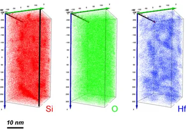
Fig. 3shows the 3D reconstructed spatial distribution of Si, O and Hf atoms in the HfSiO thin layers. Silicon and Hafnium atoms are non-homogenously distributed in the analysed volume indicat-ing clearly phase separation upon sample annealindicat-ing. The presence of Hf-rich and Si-rich zones is revealed and is consistent with the microstructure deduced from TEM experiments (Fig. 1).
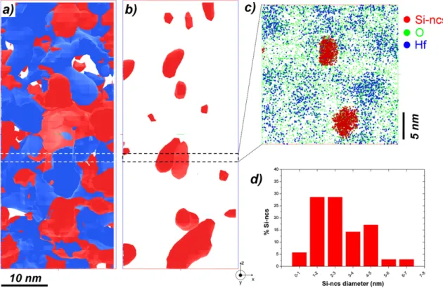
In order to identify the microstructure of the HfSiO layer and to measure the composition of the different chemical zones and their spatial distributions, we have calculated iso-concentration surface on Hf and Si atoms.Fig. 4a shows the surface for XHf> 25 at.% (in
the blue) and XSi> 33 at.% (in the red). These data provide the
evi-dence of phase separation between SiO2-rich and HfO2-rich phases
induced by the annealing treatment. Moreover, increasing the con-centration threshold of iso-concon-centration (Fig. 4b where the thresh-old are XHf> 40 at.% and XSi> 75 at.%) does not evidence Hf zones
containing more than 40 at.% but only very rich-Si clusters.Fig. 4c displays a top view in a selected region of the analysed volume which contains the different chemical zones mentioned previously. Compositions of the three chemical regions were measured and reported inTable 1. We should note that APT experiment can lead to a bias in the concentration measurement in the case of multi-phase sample analysis. This effect is due to the difference in evapora-tion field between the different phases[16]. All the concentration
Fig. 3. 3D chemical maps (Si in red, O in green and Hf in blue) of the HfSiO layer obtained by APT analyses. For clarity of the figures, only 50% of Si and O are repre-sented. The volume is 25 nm × 25 nm × 60 nm. (For interpretation of the references to color in this figure legend, the reader is referred to the web version of the article.)
Fig. 4. 3D chemical isoconcentration surfaces of hafnium and silicon extracted from the 3D chemical maps shown inFig. 3. The thresholds on Hafnium and Silicon concentration are respectively (a) XHf> 25 at.% and XSi> 33 at.%, (b) XHf> 40 at.% and XSi> 75 at.%. (c) 3D atomic mapping in selected region (dash rectangle – volume 25 nm × 25 nm × 1.5 nm).
For clarity, only silicon atoms belonging to pure Si-ncs are shown. (d) Size distribution of the Si-ncs diameter in the HfSiO layers. (For interpretation of the references to color in this figure legend, the reader is referred to the web version of the article.)
Table 1
Chemical composition in different chemical zones.
Zone XSi(at.%) XO(at.%) XHf(at.%) Phase
Hf-rich 0.0 68.2 ± 0.2 31.8 ± 0.2 HfO2
Si-rich 32.5 ± 0.2 66.2 ± 0.2 1.3 ± 0.2 SiO2
Si-ncs 98.8 ± 0.2 1.2 ± 0.2 0.0 Si-ncs
presented in this study has been corrected by applying the proce-dure developed on similar compounds by Talbot et al.[13].
The presence of a dual matrix composed of SiO2 and HfO2 is
clearly demonstrated confirming the phase separation predicted by the pseudo binary phase diagram HfO2–SiO2 which shows a
miscibility gap. In the same way, precipitation of pure Si nanoclus-ters homogenously distributed in the volume with a density of 2.9 ± 0.4 × 10¹⁷Si-ncs/cm3is also demonstrated. The Si
nanoclus-ters density was determined by counting the number of clusnanoclus-ters detected and divided it by the volume of matter analysed. Accurate size distribution of the Si nanoclusters extracted from APT analysis is presented inFig. 4d. The size ranges from 0.9 to 6.5 nm with a mean diameter of 2.8 nm.
Phase separation of hafnium silicate has been intensively stud-ied and only SiO2and HfO2formation were reported. Nevertheless,
such investigations have been performed on high content of hafnium in Hf silicate. The APT study of low content with direct evidence of Si-ncs indicates unambiguously that atomic structure of the film after thermal treatment is strongly dependant of the composition of the film.
4. Conclusion
In summary, the microstructure of high-k Hf-silicate thin lay-ers grown using magnetron sputtering was investigated by TEM
and APT. Phase separation between silica and hafnia after 950◦C
annealing was clearly evidence and leads to the growth of pure Si nanoclusters in the layer. Such Si-ncs, which have not been observed by TEM, are only revealed by APT analysis demonstrating the benefit of dual APT-TEM investigations for nanoclusters based Hf silicate materials. Moreover, these results validate reactive mag-netron sputtering approach for high-k materials elaboration and open the way to produce new nanomemory devices.
Acknowledgments
This work was supported by the Upper Normandy Region and the French Ministry of Research in the framework of Research Net-works of Upper-Normandy. The growth of the layer is supported by the French National Research Agency (ANR) through Nanoscience and Nanotechnology Program (NOMAD Project no. ANR-07-NANO-022-02) and, for one of the authors (L. Khomenkova) by the Conseil Régional de Basse Normandie through the CPER project – Nanoscience axe (2007-2013).
References
[1] S. Tiwari, F. Rana, H. Hanafi, A. Harstein, E.F. Crabbé, K. Chan, Appl. Phys. Lett. 68 (1996) 1377.
[2] G.D. Wilk, R.M. Wallace, J.M. Anthony, J. Appl. Phys. 89 (2001) 5243. [3] G.D. Wilk, R.M. Wallace, Appl. Phys. Lett. 74 (1999) 2854.
[4] M.A. Quevedo-Lopez, M. El-Bouanani, B.E. Gnade, R.M. Wallace, M.R. Visokay, M. Douglas, M.J. Bevan, L. Colombo, J. Appl. Phys. 92 (2002) 3540.
[5] L. Khomenkova, C. Dufour, P. Coulon, C. Bonafos, F. Gourbilleau, Nanotechnol-ogy 21 (2010) 095704.
[6] W. Li, R. Jia, C. Chen, M. Liu, H.F. Li, C.X. Zhu, S. Long, ECS Trans. 18 (2009) 1071. [7] S. Stemmer, Y. Li, B. Foran, P.S. Lysaght, S.K. Streiffer, P. Fuoss, S. Seifert, Appl.
Phys. Lett. 83 (2003) 3141.
[8] Y.Q. Wang, J.H. Che, W.J. Yoo, Y.C. Yeo, J. Appl. Phys. 98 (2005) 013536. [9] J. Liu, X. Wu, W.N. Lennard, D. Landheer, Phys. Rev. B 80 (2009) 041403.
720 E. Talbot et al. / Materials Science and Engineering B 177 (2012) 717–720 [10] C. Ternon, F. Gourbilleau, X. Portier, P. Voivenel, C. Dufour, Thin Solid Films 419
(2002) 5.
[11] L. Khomenkova, X. Portier, J. Cardin, F. Gourbilleau, Nanotechnology 21 (2010) 285707.
[12] D. Blavette, B. Deconihout, A. Bostel, J.M. Sarrau, M. Bouet, A. Menand, Rev. Sci. Instrum. 64 (1993) 2911.
[13] E. Talbot, R. Lardé, F. Gourbilleau, C. Dufour, P. Pareige, Europhys. Lett. 87 (2009) 26004.
[14] R. Lardé, E. Talbot, P. Pareige, H. Bieber, G. Schmerber, S. Colis, V. Pierron-Bohnes, A. Diana, J. Am. Chem. Soc. 133 (2011) 1451.
[15] G.B. Thompson, M.K. Miller, H.L. Fraser, Ultramicroscopy 100 (2004) 25. [16] D. Blavette, F. Vurpillot, P. Pareige, A. Menand, Ultramicroscopy 89 (2001) 145.