Development of Ultrashort Pulse Fiber Lasers for Optical
Communication Utilizing Semiconductor Devices
by
Erik R. Thoen
B.S. Engineering, Swarthmore College, 1995 M.S. Electrical Engineering and Computer Science,
Massachusetts Institute of Technology, 1997
Submitted to the Department of Electrical Engineering and Computer Science in partial fulfillment of the requirements for the degree of
Doctor of Philosophy in Electrical Engineering at the
MASSACHUSETTS INSTITUTE OF TECHNOLOGY June 2000
© 2000 Massachusetts Institute of Technology. All rights reserved.
Signature of Author . . . Department of Electrical Engineering and Computer Science May 19, 2000 Certified by . . . Erich P. Ippen Elihu Thompson Professor of Electrical Engineering and Computer Science Professor of Physics Thesis Supervisor
Accepted by . . . Arthur C. Smith Chairman, Committee on Graduate Students Department of Electrical Engineering and Computer Science
3
Development of Ultrashort Pulse Fiber Lasers for Optical
Communication Utilizing Semiconductor Devices
by
Erik R. Thoen
Submitted to the Department of Electrical Engineering and Computer Science in partial fulfillment of the requirements for the degree of
Doctor of Philosophy in Electrical Engineering
Abstract
The nonlinear reflectivity of semiconductor saturable absorber mirrors is investigated with ultrafast time-resolved and time-averaged reflectivity measurements. The rela-tive contributions of absorption bleaching and induced absorption are studied as a function of fluence and wavelength. The impact of induced absorption on the stability of continuous-wave mode-locking is considered theoretically. Picosecond pulses are produced from an Er/Yb waveguide laser using a semiconductor saturable absorber mirror, and the influence of two-photon absorption on mode-locking is studied. A semiconductor mirror exhibiting only induced absorption is used to stabilize a GHz repetition rate active harmonically mode-locked fiber laser, improving supermode suppression by eliminating pulse dropouts.
Thesis Supervisor: Erich P. Ippen
Title: Elihu Thomson Professor of Electrical Engineering and Computer Science Professor of Physics
ACKNOWLEDGEMENTS 5
ACKNOWLEDGMENTS
My deepest gratitude goes to Professor Erich Ippen for being a fantastic mentor, role model, and friend during my graduate studies. He has been the ideal advisor for me; I could not have found better. I can only aspire to his intuition, thoughtfulness, and kindness. Work-ing with Professor Leslie Kolodziejski has been a wonderful experience because of her high standards, honesty, and sense of humor. The close collaboration with her group has made this thesis possible. Professor Hermann Haus has been an inspiration both for his astounding the-oretical insight and endless energy. I thank all of them for supporting my research and serving on my thesis committee.
The best part of this thesis has been working with Elisabeth Koontz. This project has been truly collaborative, and without her expertise it never would have worked. I have devel-oped a deep appreciation for her technical abilities, but more important I have enjoyed her generous friendship. I thank both Elisabeth and her husband Carl for making MIT a little bit more livable.
Many other people have participated in this research, and I appreciate their contribu-tions. Professor Franz Kärtner provided key insights at critical junctures and has become a wonderful friend. Patrick Langlois and Markus Joschko did a ton of fantastic pump-probe that was critical to understanding these devices. One of the most productive students I have ever met is Thomas Schibli, who contributed greatly to our theoretical understanding of stabi-lization. David Jones started me on the waveguide laser and has blazed a path for me to fol-low ever since Swarthmore. Joe Donnelly provided expert advice on proton bombardment and has been a long-time friend, answering my countless questions. Igor Bilinsky’s com-ments prompted much of the work on TPA. Gale Petrich was always happy to help (but always had a broken pump). Denis Barbier provided the Er-Yb waveguide, Chris Cook deposited a number of evaporative coatings, and Libby Shaw and Tim McClure provided expert guidance in the CMSE Analytical Shared Experimental Facilities. I leave future work (and my office window) behind in the competent hands of Juliet Gopinath, Matt Grein, and Dan Ripin. It has been a joy coming to know Juliet and helping her discover the wonders of pump-probe measurements. Matt has been a enjoyably intriguing officemate for years, and now we have even built lasers together. Finally Dan has always offered a helping hand, gen-erated PBG results, and brought incredibly interesting lunches to the conference room.
I've learned from quite a number of other people who passed through the group over the years (before and during my time). Lynne Molter has been encouraging and supportive before and ever since I arrived at MIT. Katie Hall provided advice, equipment, lots of laughs (often with Kristin Rauchenbach), and source of revenue in the form of a book chapter. Gadi Lenz has been a great friend and source of advice since when I first visited the group. I'm still thankful that Siegfried Fleischer and Dave Dougherty put up with me as a young, optimistic, and eager grad student. Günter Steinmeyer was one of my first mentors, and I learned a great deal from him. Lynn Nelson was always generous with her time to me. I appreciate the friendship of others connected with the group including Luc Boivin, Steve Boppart, Brett Bouma, Yijiang Chen, Wolfgang Drexler, Jim Foresi, Boris Golubovic, Farzana Khatri, Ed Lim, Brent Little, Stefano Longhi, Moti Margalit, Masayuki Matsumoto, Uwe Morganer, Shu Namiki, Gaston Tudury, and William Wong. Quite a number of current group members have shared the struggle, including Pat (and Suky) Chou, John Fini, Leaf Jiang, Jalal Khan, J. P. Laine, Christina Manolatou, Milos Popovic, Peter Rakich, Mike Watts, Charles Yu, and Serhii Zhak, and the Fujimoto contingent of Seong-Ho Cho, Christian Chudoba, Ravi Ghanta, Ing-mar Hartl, Pei-Lin Hsiung, Tony Ko, Xingde Li, Costas Pitris, Rohit PrasankuIng-mar, and Kath-leen Saunders. I wish them all the best of luck in the rest if their time at MIT. I also appreciate the kindness of Mrs. Ippen and Mrs. Haus over the years. Finally, thanks go to Cindy Kopf, Donna Gale, and Mary Aldridge who all keep the group running both in terms of administration and group parties.
I am thankful for the support of the Beinecke Brothers Memorial Scholarship and Tom Parkinson, its wonderful administrator. I have also benefitted from the support of a Joint Ser-vices Electronics Program fellowship.
Outside of the lab I am grateful to a number of friends including Tom Murphy (a fabu-lous roommate for a really, really long time), James Hockenberry (godson and fellow Swat-tie), Thomas Ta (Banc-er), Nina Santos (who climbs tall buildings), Tonet Santos (The Man), Kaori Shingledecker, Joel Broveleit, Bill Hoffman, Dan Smoot, and Jen Zimmer. My thanks go out to all the people from CF, P2K (Forever!), and the whole South Dakota crew.
Finally I thank God for blessing me with wonderful parents and brothers who have watched over me, encouraged me, and supported me in everything I do. Without them, I
TABLEOF CONTENTS 7
T
ABLE OF CONTENTS
Acknowledgments
5
Table of Contents
7
List of Figures
11
Chapter 1 Introduction
19
1.1 Passively Mode-Locked Fiber Lasers... 20
1.2 Active Harmonically Mode-Locked Fiber Lasers ... 22
1.3 Semiconductor Saturable Absorbers for Mode-Locking ... 24
1.4 Outline of Thesis... 25
Chapter 2 Semiconductor Saturable Absorber Mirrors
27
2.1 Structure Design ... 272.2 Growth of Semiconductor Saturable Absorber Mirrors ... 32
2.3 Optical Characterization ... 32
Chapter 3 Time-Resolved Nonlinear Response
39
3.1 Pump-Probe Measurements ... 393.2 Fluence Dependence ... 40
3.3 Wavelength Dependence ... 44
3.5 Hot-carrier Dynamics ... 47
3.6 Below-Band Induced Absorption ... 48
3.7 Implications of Induced Absorption ... 50
Chapter 4 Time-Averaged Nonlinear Response
53
4.1 Nonlinear Reflectivity Measurements ... 534.2 Structural Design Effects ... 55
4.3 Resonant Coating Effects... 58
Chapter 5 Stabilization of Passive Mode-Locking
67
5.1 Effect of Two-Photon Absorption on Reflectivity ... 675.2 Relating Time-Averaged and Time-Resolved Measurements... 71
5.3 Mode-Locking Stabilization ... 74
Chapter 6 Erbium-Ytterbium Waveguide Laser
79
6.1 Waveguide Laser Design ... 796.2 Operation Without Filtering... 81
6.3 Absorber Operation... 83
6.4 Operation With Filtering... 84
Chapter 7 Stabilization of Harmonic Mode-Locking
91
7.1 Stabilizing Harmonically Mode-Locked Lasers ... 917.2 Laser Design ... 92
7.3 Operation Without TPA... 94
7.4 Operation With TPA... 96
7.5 Advantages of TPA... 99
TABLEOF CONTENTS 9
A.2 Fast Saturable Absorber... 107
A.3 Slow Saturable Absorber with Spatial Effects... 110
A.4 Fast Saturable Absorber with Spatial Effects ... 112
A.5 Two-Photon Absorption... 113
A.6 Time-Averaged Reflectivity ... 115
Appendix B Passively Mode-Locked Fiber Laser
117
B.1 Dispersion Management... 117B.2 Polarization Sidebands ... 118
B.3 Stabilization with Two-Photon Absorption ... 121
B.4 Absorber Lifetime Reduction... 123
Appendix C Actively Mode-Locked Fiber Laser
127
LISTOF FIGURES 11
LIST OF FIGURES
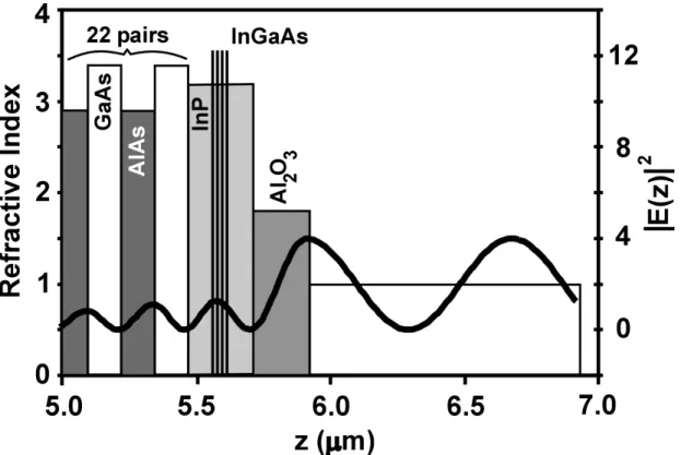
Figure 2.1 ... 28 Schematic of an anti-reflection coated semiconductor saturable absorber mirror containing two quantum wells. The refractive index and magnitude squared of the electric field (λ=1.54 mm) are plotted as a function of distance from the GaAs substrate-DBR interface.
Figure 2.2 ... 30 Schematic of an anti-reflection coated semiconductor saturable absorber mirror containing four quantum wells. The refractive index and magnitude squared of the electric field (λ=1.54 mm) are plotted as a function of distance from the GaAs substrate-DBR interface.
Figure 2.3 ... 31 Schematic of a resonantly coated semiconductor saturable absorber mirror con-taining four quantum wells. The refractive index and magnitude squared of the electric field (λ=1.54 mm) are plotted as a function of distance from the GaAs substrate-DBR interface.
Figure 2.4 ... 31 Schematic of an anti-reflection coated semiconductor saturable absorber mirror containing a quasi-bulk absorption region. The refractive index and magnitude squared of the electric field (λ=1.54 mm) are plotted as a function of distance from the GaAs substrate-DBR interface.
Figure 2.5 ... 33 Transmission as a function of wavelength for a two quantum well structure de-posited on GaAs.
Figure 2.6 ... 34 Transmission as a function of wavelength for various quantum well structures deposited on GaAs. For comparison, the room temperature photoluminescence of each structure is also plotted in arbitrary intensity units, with an arrow indi-cating the peak
Figure 2.7 ... 35 Transmission as a function of wavelength for a typical GaAs/AlAs DBR. For comparison the normalized photoluminescence intensity of a quantum well structure deposited on GaAs is plotted.
Figure 3.1 ... 41 Differential reflectivity measurements as a function of excitation fluence at 1.5 µm. At low fluence, the bleaching dynamics of the QWs are dominant. At higher fluences, TPA and FCA develop and eventually dominate the ultrafast dynamics.
Figure 3.2 ... 43 Differential reflectivity measurements as a function of excitation fluence at 1.54 µm. The change of reflection ∆R/R0 = (R - R0)/R0 (R, R0: reflection with and
without pump, respectively) is plotted versus delay between pump and probe pulses. The autocorrelation (AC) depicts the temporal resolution.
Figure 3.3 ... 44 Differential reflectivity measurements under high fluence excitation as a func-tion of wavelength. The wavelength is tuned from above to below the QW bandgap (~1.53 µm). Below the QW bandgap, TPA and FCA in InP are domi-nant.
Figure 3.4 ... 45 Differential reflectivity measurements for a pump fluence of 250 µJ/cm2 with the probe fluence varied as indicated.
Figure 3.5 ... 46 Differential reflectivity measurements at a pump fluence of 320 µJ/cm2 for low (solid curve) and high (dashed curve) probe fluence, and the difference between the two (dash-dotted curve).
Figure 3.6 ... 48 Differential reflectivity measurements with excitation by Ti:sapphire pulses for a saturable absorber mirror with low (solid curve) and high (dashed curve)
LISTOF FIGURES 13
Figure 3.7 ... 49 Differential reflectivity measurements under high fluence excitation at 1.56 µm for a saturable absorber mirror structure in which absorption bleaching is neg-ligible (solid curve). The ~5 ps decay for FCA is attributed to carrier diffusion across the InP half-wave layer. The dashed curve shows the differential absorp-tion of a ~350 µm thick InP substrate in which a standing-wave pattern is not formed. Inset: linear and quadratic fluence dependence of the TPA and FCA components respectively, in the saturable absorber mirror structure.
Figure 4.1 ... 54 Transmitted power has a function of knife-edge position in the beam after pass-ing through a focuspass-ing lens. The fit to an error function provides the Gaussian width.
Figure 4.2 ... 55 The beam waist as a function of distance from a focusing lens as determined from several knife-edge measurements. The fit of the waist as a function of po-sition gives the focused spot size
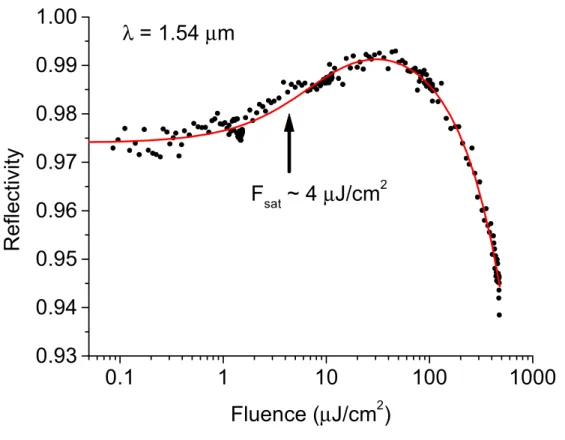
Figure 4.3 ... 56 Measured reflectivity as a function of fluence at 1.542 microns for an antireflec-tion coated sample similar to the structure of Figure 2.2 except containing six quantum wells. The solid line is the result of a fit to a slow saturable absorber model with the coefficients indicated.
Figure 4.4 ... 57 Measured reflectivity as a function of fluence at 1.542 microns for the antire-flection coated structure of Figure 2.4. The solid line is the result of a fit to a slow saturable absorber model with the coefficients indicated.
Figure 4.5 ... 59 Measured reflectivity as a function of fluence at 1.542 microns for the antire-flection coated structure of Figure 2.2. The solid line is the result of a fit to a slow saturable absorber model with the coefficients indicated.
Figure 4.6 ... 60 The reflectivity as a function of wavelength of the resonantly coated structure of Figure 2.3 (solid line) and a DBR mirror (dashed line) measured with a Fou-rier transform infrared spectrometer.
Figure 4.7 ... 61 The total change in reflection as a function of wavelength for the structure of Figure 2.3. The measurement was performed with a single 20 cm lens. The sol-id line is a Gaussian fit to the data.
Figure 4.8 ... 62 Measured reflectivity as a function of fluence at 1.5 microns for the resonantly coated structure of Figure 2.3. The solid line is the result of a fit to a slow sat-urable absorber model with the coefficients indicated.
Figure 4.9 ... 63 Measured reflectivity as a function of fluence at 1.53 microns for the resonantly coated structure of Figure 2.3. The solid line is the result of a fit to a slow sat-urable absorber model with the coefficients indicated.
Figure 4.10 ... 64 Predicted variation in the saturable loss as a function of wavelength for the structure of Figure 2.3. The data points are taken from Figures 4.8 and 4.9 and extrapolated from Figure 4.8, and the solid line is a Gaussian fit.
Figure 4.11 ... 64 Predicted variation in the saturation fluence as a function of wavelength for the structure of Figure 2.3. The data points are taken from Figures 4.8 and 4.9 and extrapolated from Figure 4.8, and the solid line is a Gaussian fit.
Figure 4.12 ... 65 Predicted variation in the AStruct parameter as a function of wavelength for the structure of Figure 2.3. The data points are taken from Figures 4.8 and 4.9 and extrapolated from Figure 4.8, and the solid line is a Gaussian fit.
Figure 5.1 ... 69 Saturation fluence measurements at 1.5 microns for the antireflection coated structure of Figure 2.1. The solid line is a fit using the model described in Sec-tion 5.3. The inset depicts the time-resolved differential reflectivity measured at ~80 µJ/cm2.
Figure 5.2 ... 70 Saturation fluence measurements 1.5 microns for the antireflection coated structure of Figure 2.3. The solid line and dashed lines are calculated using the model described in Section 5.3. The insets depict the time-resolved differential reflectivity measured at (i) ~10 µJ/cm2 and (ii) ~200 µJ/cm2.
Figure 5.3 ... 72 The change in reflectivity as a function of fluence at 1.54 microns for the anti-reflection coated sample of Figure 2.2 as obtained from pump-probe measure-ments at zero delay. (Open squares - low fluence probe, filled circles - high
LISTOF FIGURES 15
Figure 5.5 ... 74 The change in reflectivity as a function of fluence at 1.54 microns for the anti-reflection coated sample of Figure 2.2 as obtained from pump-probe measurements at a delay of 2.5 ps. (Open squares low fluence probe, filled circles -high fluence probe, filled triangles - subtracted)
Figure 5.6 ... 76 Effect of optical limiting on mode-locking stability. In the presence of TPA, following a perturbation the pulse envelope returns to a CWML state (dashed line). In the absence of TPA, following a perturbation the pulse envelope enters a QSML state (solid line).
Figure 5.7 ... 77 Calculated stability contours for a fast saturable absorber mode-locked laser. QSML is present in the regions labeled "unstable". CWML is present in the re-gions labeled "stable". The area within the solid line is the instability region without TPA included in the model. The area within the dashed line is the in-stability region with TPA included in the model.
Figure 6.1 ... 80 Schematic of the laser cavity based on an Er-Yb planar waveguide. The dotted box surrounds the filtering elements.
Figure 6.2 ... 82 Second harmonic generation autocorrelation of the pulses obtained with the cavity configuration of Figure 6.1 without filtering (data – solid, sech fit – dashed).
Figure 6.3 ... 82 Optical spectrum centered at 1534 nm of the pulses obtained with the cavity configuration of Figure 6.1 without filtering.
Figure 6.4 ... 84 The semiconductor saturable absorber mirror reflectivity measured as a func-tion of incident energy fluence with 150 fs pulses at 1530 nm (dots). The solid lines are the saturable absorption (SA) and two-photon absorption (TPA 150 fs) components fit to the measured data. The dotted (TPA 9 ps) and dashed (TPA 1 ps) lines are calculated TPA components. The shaded region depicts the range of fluences where CWML was obtained with 9.8 ps pulses.
Figure 6.5 ... 85 Fluorescence of erbium-doped fiber as a function of pump power.
Figure 6.6 ... 85 Fluorescence of the erbium-ytterbium waveguide as a function of pump power.
Figure 6.7 ... 87 Second harmonic generation autocorrelation of the pulses obtained with the cavity configuration of Figure 6.1 with filtering (data – filled circles, sech fit – solid line).
Figure 6.8 ... 87 Optical spectrum centered at 1545 nm of the pulses obtained with the cavity configuration of Figure 6.1 with filtering.
Figure 6.9 ... 88 Optical spectrum of tunable pulses obtained at 100 MHz in the cavity configu-ration of Figure 6.1 by adjusting the bandedge filter.
Figure 7.1 ... 93 Schematic of an anti-reflection coated two-photon absorption mirror containing an ~5.2 micron thick InP layer. The refractive index and magnitude squared of the electric field (λ=1.54 mm) are plotted as a function of distance from the GaAs substrate-DBR interface.
Figure 7.2 ... 93 Schematic of actively mode-locked fiber laser. Wavelength division multiplex-er (WDM), Erbium-doped fibmultiplex-er (EDF).
Figure 7.3 ... 94 Second harmonic generation autocorrelation of the pulses obtained without fo-cusing on TPA mirror.
Figure 7.4 ... 95 Optical spectrum of the pulses obtained without focusing on TPA mirror. Figure 7.5 ... 95
Rf spectrum of output pulses obtained without focusing on TPA mirror. Reso-lution bandwidth of 30 kHz.
Figure 7.6 ... 96 Digitizing oscilloscope trace obtained without focusing on TPA mirror exhibit-ing dropouts of output pulses.
Figure 7.7 ... 97 Second harmonic generation autocorrelation of the pulses obtained with focus-ing on TPA mirror.
LISTOF FIGURES 17
Figure 7.10 ... 99 Digitizing oscilloscope trace obtained with focusing on TPA mirror exhibiting no pulse dropouts is shown in the upper trace. The detector and instrument noise background in the absence of the optical input is shown in the lower trace. Figure B.1 ... 118 Schematic of fiber laser. Wavelength Division Multiplexer (WDM), Erbium Doped Fiber (EDF), Single-Mode Fiber (SMF).
Figure B.2 ... 119 Optical spectrum obtained for anomalous dispersion operation.
Figure B.3 ... 120 Optical spectrum obtained for slightly normal dispersion operation.
Figure B.4 ... 121 Optical spectrum for various intracavity quarter-wave-plate settings. From top to bottom the wave-plate is varied in five degree increments.
Figure B.5 ... 122 Optical spectrum through a polarizing beam splitter with various external-cav-ity half-wave-plate settings. From top to bottom the wave-plate is varied from 45 to 0 degrees.
Figure B.6 ... 123 Spectral width versus pulse energy for a soliton fiber laser mode-locked with saturable absorber mirrors having different thicknesses of InP.
Figure B.7 ... 124 Spectral width and number of pulses versus pump current for a soliton fiber la-ser mode-locked with a saturable absorber mirror.
Figure B.8 ... 125 Autocorrelations of a bunched multiple pulse state at several pump currents. From bottom to top the pump current is 390, 475, 550, and 650 mA.
Figure B.9 ... 126 Autocorrelation of a bunched multiple pulse state with an exponential fit of the long background envelope.
Figure C.1 ... 128 Schematic of active harmonically mode-locked linear laser. Wavelength Divi-sion Multiplexer (WDM).
Figure C.2 ... 129 Low frequency operation. Optical spectrum (Top) and autocorrelation (Bot-tom).
Figure C.3 ... 130 High frequency operation. Optical spectrum (Top) and autocorrelation (Bot-tom).
INTRODUCTION 19
CHAPTER 1
INTRODUCTION
The explosive growth of the Internet has recently driven the development of optical communications. To meet the increasing bandwidth demands, both wavelength-division mul-tiplexing (WDM) [14, 81] and time-domain mulmul-tiplexing (TDM) [13, 5] are being investi-gated with ever increasing numbers of channels and higher bit rates. Fiber lasers play an important role in the development of telecommunications systems. Active harmonically mode-locked fiber lasers have been developed at very high repetition rates and have been used as pulse sources in high bit-rate system demonstrations in a research setting [25]. Passively mode-locked fiber lasers exhibiting sub-picosecond pulses have been developed, and the cor-responding broad spectrum has been used for a variety of applications including spectral slic-ing [8], optical coherence tomography [9], and solid-state amplifier seedslic-ing [75].
This thesis focuses on the use of semiconductor structures to improve the characteris-tics of passively and actively mode-locked fiber and waveguide lasers. Obtaining self-starting mode-locking, suppressing Q-switched mode-locking, and attaining high repetition rates can all be difficult in a passively mode-locked fiber laser. In active harmonically mode-locked fiber lasers, stabilization against energy fluctuations is a significant challenge. Nonlinear semiconductor mirrors offer potential solutions for a number of the problems in passively and actively mode-locked fiber lasers.
1.1
Passively Mode-Locked Fiber Lasers
Three primary methods have been used to passively mode-locked fiber lasers. Nonlin-ear polarization rotation, also known as polarization additive pulse mode-locking (P-APM), has been used to generate 63 fs pulses, the shortest from an Er-doped fiber laser [111]. P-APM is based on the intensity-dependent rotation of the polarization state in optical fiber [46, 80, 106]. The polarization state of the peak of the pulse will change differently than the wings of the pulse, so the transmission of a pulse through a polarizer can be adjusted with wave-plates to eliminate the wings of a pulse. P-APM acts as a fast saturable absorber because the Kerr effect in optical fiber is virtually instantaneous. Nonlinear polarization rotation has been used to mode-lock a wide range of fiber lasers to produce femtosecond pulses [32, 108, 109, 110, 88, 74, 89].
The nonlinear amplifying loop mirror (NALM) is a second technique for mode-lock-ing fiber lasers which is also based on the Kerr effect in fiber [31, 94, 28]. The NALM is a fiber Sagnac interferometer with the gain medium placed asymmetrically in the loop. Because of the asymmetry, a pulse traveling in one direction undergoes greater polarization rotation than a pulse traveling in the reverse direction. With proper biasing of the incident polarization, the NALM transmits high-intensity while reflecting low intensity, producing a fast saturable absorber. Pulses as short as 98 femtoseconds have been generated in an Er-doped fiber laser with an NALM [85].
Semiconductor saturable absorbers have also been used to either initiate other pulse shaping mechanisms (such as P-APM) or to serve as the primary mode-locking mechanism in fiber lasers. A semiconductor absorber was used in a fiber laser for the first time in 1991 in a transmission geometry [129]. Later a linear cavity incorporating a semiconductor saturable absorber deposited on a semiconductor Bragg reflector produced sub-picosecond pulses [76, 77]. Because a semiconductor saturable absorber can insure self-starting, combining a semi-conductor saturable absorber with P-APM has been used to generate 330 fs pulses [47]. Finally, mode-locking with a semiconductor saturable absorber does not require the long interaction lengths to produce polarization rotation, so shorter cavities are possible. Using a semiconductor Bragg reflector in a linear Er/Yb fiber laser, fundamental repetition rates as
INTRODUCTION 21
both prevent self-starting of mode-locking. To overcome these difficulties, ring cavities instead of standing-wave cavities have been implemented [107], especially for fiber lasers mode-locked with only nonlinear polarization rotation or an NALM. However semiconductor saturable absorbers have been used successfully in linear cavities, either as the primary mode-locking mechanism [16] or as a self-starting mechanism [47]. Semiconductor saturable absorbers offer a great potential for overcoming self-starting difficulties in fiber lasers because their properties can be tailored to the cavity.
A second obstacle to attaining a continuous-wave mode-locked (CWML) laser is the tendency for many lasers to Q-switch at the relaxation oscillation frequency. The stability condition for CWML over Q-switching has been derived analytically in a perturbational anal-ysis [43]. The theory has been expanded to include the stability of CWML against Q-switch-ing mode-lockQ-switch-ing (QSML) [QSML consists of a burst of ultrashort pulses with a Q-switchQ-switch-ing envelope.] [60]. Stability in the presence of soliton-shaping effects has been derived [87]. Stabilization against QSML with a semiconductor saturable absorber has also been considered for both the picosecond and femtosecond regime [48]. In terms of laser parameters, prevent-ing Q-switchprevent-ing instabilities is more difficult for shorter cavities and longer upper-state life-times. Semiconductor saturable absorbers have been used quite successfully to mode-lock even lasers with long upper-state lifetimes, because a number of parameters can be controlled [63, 64, 16]. The long upper-state lifetime of erbium (~10 ms [95]) makes Q-switching an acute problem in fiber lasers, so the proper design of a semiconductor saturable absorber mir-ror is particularly important.
The use of a reverse saturable absorber has also been proposed to suppress Q-switch-ing in lasers. Originally, a reverse saturable absorber based on excited-state absorption was suggested as an intensity limiter for preventing Q-switching [41]. Later the effect of a time constant in the reverse saturable absorber was studied in fast and slow regimes [11]. Experi-mentally, two-photon absorption (TPA) in a GaAs platelet was used to stabilize the output of a Nd:YAG laser [23]. The same technique was used to stabilize an actively mode-locked Nd:YAG laser [79]. In the context of fiber laser gain media exhibiting a long upper-state life-time, intensity-limiting mechanisms could be quite useful for stabilization against Q-switch-ing.
A third major difficulty in designing fiber lasers is that the doping density of erbium in silica-based fibers is typically quite low, requiring very long lengths (meters) of fiber for suf-ficient gain in a laser [84]. While solid-state lasers have been mode-locked at fundamental repetition rates in the GHz regime [68], fiber lasers have not been demonstrated with funda-mental repetition rates above a few hundred MHz because of the long lengths of doped fiber
required [16]. Recently erbium-doped planar waveguide amplifiers have been introduced with significantly higher doping densities than silica fiber [90]. A 4.5 cm Er-Yb phosphate glass waveguide has been used as an amplifier in system experiments at 10 Gb/s with 16.5 dB gain [22]. A similar waveguide was operated as a continuous-wave laser producing output powers greater than 2 mW [125]. With the incorporation of a modulator into the cavity, a Q-switched laser was demonstrated with kW peak powers [126]. However, none of these designs have taken advantage of the short length of Er-Yb waveguides to produce a high repe-tition rate fundamentally mode-locked laser.
A number of obstacles remain in the development of advanced passively mode-locked fiber lasers, but potential solutions also exist. Semiconductor saturable absorber mirrors are one solution to self-starting difficulties in fiber lasers. Properly designed semiconductor structures might also be useful for suppressing Q-switching instabilities in long upper-state lifetime lasers. Finally Er-Yb waveguides offer one method for producing significantly shorter fundamental cavity round-trip times, and when combined with a semiconductor satu-rable absorber, waveguide lasers could produce ultrashort pulses, high repetition-rate sources.
1.2
Active Harmonically Mode-Locked Fiber Lasers
One method to attain very high repetition rates (>GHz) is to operate a laser harmoni-cally, such that multiple pulses are present in the cavity at one time. A high-speed electro-optic modulator is driven at a harmonic of the round-trip time of the cavity, creating multiple pulse slots in the cavity. With this active mode-locking technique, the repetition rate is no longer dictated by the fundamental length of the cavity. Such a laser has the additional advan-tage that the repetition rate is controlled by an electronic frequency synthesizer, so the pulses can be "locked-to-clock," an important functionality in a communications system. This tech-nique has been applied to fiber lasers to generate 6 ps pulses at 40 GHz [93]. Improvements have been made to generate sub-picosecond pulses tunable across the Er bandwidth at 40 GHz [128], and the output could be scaled to 160 Gb/s [30]. The harmonic mode-locking tech-nique has been used quite successfully to produce fiber laser sources that are useful in a research setting.
INTRODUCTION 23
monic and its integer multiples are excited. A group of equally spaced axial modes in the fre-quency domain is referred to as a supermode [103]. In the presence of fluctuations, supermodes other than integer multiples of the harmonic frequency are excited. The degree of fluctuations can be quantified by the supermode suppression in the radio frequency spectrum of the pulse train. Supermode suppression >50 dB is generally considered sufficient for com-munications applications.
One of the first techniques used to stabilize a harmonically mode-locked fiber laser involved controlling the cavity length. The length of the cavity was adjusted by stretching fiber with a PZT to match the phase of the cavity round-trip time to that of the oscillator driv-ing the electro-optic modulator [100]. Later modifications of this technique involved dither-ing the cavity length [101] or detectdither-ing noise at frequencies other than the mode-locked harmonic [102]. Given the thermal sensitivity of optical fiber, the fundamental cavity round-trip time will drift with temperature variations, so some type of cavity length stabilization is required for any harmonically mode-locked fiber laser to be stable over a long period of time. However, techniques used to stabilize supermodes with cavity-length control require more complicated signal processing [102] than simply matching the phase of the oscillator and out-put pulses.
A second technique to suppress supermodes involves introducing an additional cavity into the laser (a ring sub-cavity or Fabry Perot) with a free spectral range matching the repeti-tion rate [127, 42]. In the frequency domain, the filter prevents the excitarepeti-tion of modes other than the harmonic at which the laser is operated. In the time domain this corresponds to equalizing energy across all the pulses. The primary difficulty with this technique is that the cavity length and sub-cavity free spectral range must be stabilized to match one another. In a practical system the cavity length would be matched to the modulation frequency and the sub-cavity would also be matched to that frequency. With both the length control technique and the sub-cavity technique, active stabilization is required, so passive solutions would clearly offer advantages.
A third method for stabilizing harmonically mode-locked lasers employs polarization rotation to produce a fast intensity-dependent loss. As described in the previous section, polarization rotation in a fiber is intensity dependent, so when combined with polarization control and a polarizer, an artificial fast saturable absorber can be created. However with proper adjustment of the polarization, intensity-dependent limiting can also be produced, which is referred to as additive-pulse limiting (APL) [26]. The technique was used success-fully to produce a stable 1-GHz harmonically mode-locked laser. However because the tech-nique is dependent on polarization rotation, thermal drift of the fiber inducing linear
polarization rotation leads to bias drift, therefore foiling APL. A passive technique not sensi-tive to environmental conditions is more desirable.
An additional passive technique for supermode suppression employs self-phase modu-lation and spectral filtering, which creates peak intensity limiting similar to APL [86]. By vir-tue of the nonlinearity in optical fiber, as a pulse propagates its spectrum is broadened in proportion to its peak intensity by self-phase modulation. If a spectral filter is introduced after such broadening, then a higher peak intensity pulse exhibiting a broader spectrum is filtered more strongly then a lower peak intensity pulse exhibiting a narrower spectrum. This tech-nique has been used successfully to suppress supermodes by >50 dB in a 10 GHz fiber laser [86]. However, because the energy is distributed among a large number of pulses in a har-monically mode-locked fiber laser, the peak intensity of individual pulses is relatively low. To obtain the required spectral broadening for supermode suppression the interaction length must be enhanced, requiring a cavity hundreds of meters long. A further limitation of this tech-nique is that it only works in the anomalous dispersion regime, limiting its applicability to soliton lasers [112].
All of the techniques presented for stabilizing harmonically mode-locked fiber lasers exhibit some disadvantages. The active techniques require significant external circuitry. For passive techniques, APL is environmentally unstable and self-phase modulation (SPM) with filtering requires very long cavities and anomalous dispersion. A semiconductor structure which could provide a fast intensity-dependent loss with a small footprint would be particu-larly attractive for stabilizing supermodes.
1.3
Semiconductor Saturable Absorbers for Mode-Locking
Semiconductor saturable absorber structures offer a potential solution to a number of the problems encountered in both passively and actively mode-locked fiber lasers. Semicon-ductor nonlinearities were used to passively mode-lock a semiconSemicon-ductor laser for the first time 20 years ago [49]. Later, but still more than a decade ago, a semiconductor saturable absorber was first applied to mode-locking a solid-state color-center laser [51]. However in both of
INTRODUCTION 25
shortly afterwards [63]. A semiconductor saturable absorber mirror, termed a saturable Bragg reflector (SBR), which requires no growth post-processing has also been used as an intracav-ity saturable absorber in a variety of solid-state lasers [122]. Some of the shortest pulses ever attained (<6 fs, in the two-cycle regime) were produced from a Kerr-lens mode-locked Ti:sap-phire with an intracavity semiconductor saturable absorber mirror [105]. Variations on all of these designs have been used to mode-locked a wide range of solid-state and fiber lasers [64, 65, 16].
For fiber lasers in particular, semiconductor saturable absorber mirrors offer a number of advantages. A semiconductor saturable absorber can be used to obtain repeatable self-start-ing in a fiber laser, even when another mechanism may be used for pulse shapself-start-ing. The prop-erties of a semiconductor saturable absorber can be designed to enhance the stability of a fiber laser against QSML. As a mode-locking mechanism, a semiconductor saturable absorber does not require the interaction length of nonlinear polarization rotation or an NALM, so it is usable with very short cavities. For actively mode-locked systems, semiconductor structures may be used to provide optical limiting to stabilize against unwanted supermodes. Therefore leveraging on the established base of semiconductor saturable absorber mirror technology, this thesis investigates a number of new applications of semiconductor structures to fiber and waveguide lasers.
1.4
Outline of Thesis
The thesis is organized as follows. In Chapter 2 the basic design of the semiconductor saturable absorber mirrors used throughout this thesis is discussed. A short description of the gas source molecular been epitaxial growth technique used to create the structures follows. Finally the basic optical techniques used to initially characterize the properties of the semi-conductor layers are discussed.
Chapter 3 presents an investigation of the time-resolved nonlinear response of the semiconductor structures. Pump-probe measurements as a function of fluence and wave-length are shown, and the corresponding ultrafast nonlinear dynamics are discussed. More detailed studies of induced absorption both above- and below-band are presented along with two-color experiments used to investigate hot-carrier dynamics. The implications of induced absorption on mode-locking of lasers are discussed briefly.
The measurements of the time-averaged nonlinear response of the semiconductor satu-rable absorber mirrors are discussed in Chapter 4. The details of the technique used to
mea-sure the nonlinear reflectivity are presented along with meamea-surements of a wide range of structures. The impact of structural design and post-growth optical coatings on the nonlinear reflectivity is discussed in detail for a number of cases.
In Chapter 5 the impact of induced absorption on mode-locking is discussed. Initially the role of two-photon absorption on the nonlinear reflectivity of the various structures is investigated. The time-averaged and time-resolved reflectivity are compared to clarify the physical mechanisms responsible for changes in reflectivity. Finally the theoretical impact of induced absorption on mode-locking stability is presented.
The results of mode-locking an Er-Yb waveguide laser using a semiconductor satura-ble absorber mirror are presented in Chapter 6. The design and operation of the laser without an intracavity filtering element is presented, and the effect on mode-locking of two-photon absorption in the absorber structure is studied. Intracavity filtering is investigated and shown to produce significantly shorter pulses.
Stabilization of an active harmonically mode-locked fiber laser with a semiconductor mirror is described in Chapter 7. The design of the laser and operation without two-photon absorption is studied initially. Then the stabilizing effect of a two-photon absorbing semicon-ductor mirror is investigated, and the advantages of using two-photon absorption over other stabilizing techniques are discussed.
Appendix A outlines the mathematical details of the various models for the nonlinear reflectivity used throughout the thesis. Cases of both slow and fast saturable absorbers are considered, and the impact of a Gaussian beam distribution is considered.
Results from a passively mode-locked fiber laser are discussed in Appendix B. Issues of dispersion management, polarization sidebands, stabilization with two-photon absorption, and lifetime reduction are investigated.
Appendix C presents preliminary results of active harmonic mode-locking of a fiber laser in a linear geometry using a travelling-wave phase modulator.
Finally Chapter 8 presents the conclusions of the thesis, and outlines various areas for future work.
SEMICONDCUTOR SATURABLE ABSORBER MIRRORS 27
CHAPTER 2
SEMICONDUCTOR SATURABLE ABSORBER MIRRORS
In this chapter1 the results are presented of studies performed on a variety of semicon-ductor saturable absorber mirrors designed for different applications. Depending on the appli-cation, variations in the design of the structure including placement of the absorbing region, amount of absorbing material, and optical coatings were investigated. The design, growth, and basic optical characterization of the devices is discussed here.
2.1
Structure Design
All of the semiconductor structures considered in this thesis consist of a distributed Bragg reflector (DBR) with additional top layers producing saturable absorption or induced absorption. The structures are tailored to the requirements of particular lasers. Depending on the design of the absorbing layers and additional coatings, the amount of saturable loss, the amount of induced absorption, the amount of non-saturable loss, the wavelength dependence, and the saturation fluence can be controlled.
Initial design of a structure involves calculating the electric field profile within the structure using matrix and interface techniques [7]. One example of such a calculation is shown in Figure 2.1, where the magnitude of the electric field as a function of position is ted on the right axis. On the left axis the refractive index of the various material layers is
plot-1 Many of the results of this chapter were attained in collaboration with Elisabeth M. Koontz, Prof. Franz X. Kärtner, and Prof. Leslie Kolodziejski. Optical coatings were provided by Chris Cook of Lincoln Lab-oratory and assistance with the spectrophotometer was provided by Elisabeth L. Shaw of the Analytical Shared Experimental Facilities, MIT Center for Materials Science and Engineering.
ted as a function of position. This structure is similar to that demonstrated by other research groups for mode-locking solid-state lasers [15]. From left to right in the figure, the last few pairs of the 22 pair GaAs/AlAs λ/4 DBR stack used to produce a high reflector centered at ~1.55 microns are shown. Next is a λ/2 layer which contains the saturable absorbing material. In the case of Figure 2.1 this layer consists of a λ/2 layer of InP with two InGaAs quantum wells located ~15 nm from the top surface of the layer. The last layer is a λ/4 thickness of Al2O3 which acts as an antireflection coating.
In Figure 2.1 the electric field magnitude squared is depicted; to obtain the intensity, the electric field magnitude squared would be multiplied by a term proportional to the refrac-tive index, which would lead to discontinuities in the plot of the intensity. Inspection of the field may be somewhat misleading because of the large index difference between air, n=1, and
Figure 2.1 Schematic of an anti-reflection coated semiconductor saturable absorber mirror containing two quantum wells. The refractive index and magnitude squared of the electric field (λ=1.54 µm) are plotted as a function of distance from the GaAs substrate-DBR interface.
SEMICONDCUTOR SATURABLE ABSORBER MIRRORS 29
The electric field in Figure 2.1 is calculated for the single wavelength of 1.54 microns. Because all of the layers of the structure are designed for a particular center wavelength, the positions of the peaks and nulls of the electric field will change with wavelength. In saturable absorber design, the most critical information that the electric field calculation provides is the overlap between the field and the absorbing region. For the structure shown in Figure 2.1, the absorbing quantum wells are located near the surface of the structure, close to a null of the electric field. With such simulations one can evaluate the placement of absorbing regions as a function of operating wavelength and desired absorbing properties.
Figure 2.2 illustrates a second structure similar to that of Figure 2.1, except the posi-tion and number of quantum wells has been altered. In this case four quantum wells instead of two are used, which increases the amount of available saturable absorption. Moving the posi-tion of the absorbing quantum wells from the null of the electric field to the peak of the field lowers the saturation fluence. The saturation fluence is the energy density at which the absorption is nearly bleached. As mentioned previously, because the position at which the electric field peaks is dependent on wavelength, the saturation fluence is also dependent on wavelength.
The absorption properties of structures may also be altered significantly based on the choice of top coating [63, 65]. Figure 2.3 illustrates the same semiconductor structure as Fig-ure 2.2, except the structFig-ure is coated with multiple layers of Si and Al2O3 instead of a single λ/4 layer of Al2O3. In this case the coating has been designed to produce a resonant field in
the InP layer. A Fabry Perot is formed between the DBR back mirror and the top coating which acts as a 70 % reflector. The field calculation shows that the magnitude squared of the field in the InP is comparable to the magnitude-squared field incident upon the structure, enhancing the intensity in the InP by roughly 3 times over the incident intensity. Such field enhancement lowers the saturation fluence significantly and increases the saturable absorption modulation depth of the structure.
Instead of the resonant coating shown in Figure 2.3, an antiresonant coating could be applied [10]. Such a coating may be desirable in solid-state lasers in which the intracavity power can be very high. Additionally in high-Q laser cavities, only a very small modulation depth of saturable absorption may be necessary to mode-lock the laser, so antiresonant coat-ings are an option. An antiresonant coating produces less intensity in the absorbing region than is incident on the structure. One special case of an antiresonant structure is an uncoated structure, often referred to as a saturable Bragg reflector [122]. Because the top surface of the structure is a high-index semiconductor, the Fresnel reflection off the top surface is reasonably large (~30 %), producing an antiresonance.
Instead of quantum wells, thicker layers of absorbing material could be used as illus-trated in Figure 2.4. In this structure the region which contained quantum wells in the previ-ous structures is now a single layer of InGaAs. Depending on the thickness of the material, it may or may not exhibit quantum confinement effects, which alter the absorption characteris-tics. The structure of Figure 2.4 exhibits significantly more saturable absorption than the structure of Figure 2.2, simply because more absorbing material is included. Although in the various devices illustrated here only single λ/2 absorbing layers have been shown, signifi-cantly thicker absorbing regions could be deposited on the DBR stack to produce larger absorption.
Considering the structures illustrated here, a variety of design parameters may be altered to control the response of semiconductor saturable absorber mirrors. The placement of the absorbing layers in the electric field standing wave can control the saturation fluence.
Var-Figure 2.2 Schematic of an anti-reflection coated semiconductor saturable absorber mirror containing four quantum wells. The refractive index and magnitude squared of the electric field (λ=1.54 µm) are plotted as a function of distance from the GaAs substrate-DBR interface.
SEMICONDCUTOR SATURABLE ABSORBER MIRRORS 31
Figure 2.3 Schematic of a resonantly coated semiconductor saturable absorber mirror containing four quantum wells. The refractive index and magnitude squared of the electric field (λ=1.54 µm) are plotted as a function of distance from the GaAs substrate-DBR interface.
Figure 2.4 Schematic of an anti-reflection coated semiconductor saturable absorber mirror containing a quasi-bulk absorption region. The refractive index and magnitude squared of the electric field (λ=1.54 µm) are plotted as a function of distance from the GaAs substrate-DBR interface.
2.2
Growth of Semiconductor Saturable Absorber Mirrors
A much more detailed description of the growth techniques used to produce the struc-tures described in this thesis is given elsewhere [67]. However because an understanding of the growth techniques is necessary for proper design of the structures, some issues will be addressed here. All of the structures discussed in this thesis were deposited by gas source molecular beam epitaxy (GSMBE) by Elisabeth M. Koontz in the laboratory of Professor Leslie A. Kolodziejski.
A somewhat unusual characteristic of the structures shown in Figures 2.1-2.4 is the GaAs-InP interface, because a large lattice mismatch exists between the two materials. In epi-taxial growth, for the highest quality material, the structure should be lattice matched. A semiconductor saturable absorber mirror containing InGaAs could be grown in a lattice matched fashion if the DBR mirror was produced from InP-based material. However because of the reduced index contrast, such a DBR would exhibit a reduced reflectivity bandwidth compared to a structure fabricated from GaAs and AlAs. Therefore in the devices developed in this thesis GaAs/AlAs DBRs are used.
Because of the lattice mismatch at the interface of the GaAs and InP, defects are cre-ated. High-quality crystalline InP/InGaAs material, with minimal defects, exhibits a very long (ns) lifetime, which may not recover between incident pulses [33]. For mode-locking applications, the defects produced by such a lattice mismatch have the fortuitous benefit of shortening the recombination time. However, defects also smear the bandedge of the material and correspondingly broaden the photoluminescence spectrum. For the applications of this thesis such smearing is not problematic because it is possible to operate within the absorption edge of the structure, so the defects are actually a benefit, because they reduce the recombina-tion time.
The epitaxial deposition for this thesis was typically performed in stages. First, the DBR structure was grown either by GSMBE or purchased from a metalo-organic chemical vapor deposition (MOCVD) facility. Second, the top absorbing layers were deposited via GSMBE on smaller pieces of the DBR structures. In some cases further growth was per-formed via GSMBE to add additional InP material. After epitaxial growth, evaporative coat-ings were deposited to enhance absorber characteristics, as detailed above.
SEMICONDCUTOR SATURABLE ABSORBER MIRRORS 33
position and thickness of the saturable absorbing layers must be controlled. Room tempera-ture photoluminescence was used to calibrate the epitaxial growth to obtain the desired absorption edge. The photoluminescence peak was also compared to wavelength dependent transmission measurements to quantify the absorption depth and sharpness of the bandedge.
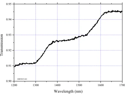
An example of the wavelength dependent transmission properties of a quantum well structure is illustrated in Figure 2.5. Two quantum wells within a λ/2 layer of InP were depos-ited on a GaAs wafer for characterization purposes. The wavelength dependent transmission was characterized in a dual-arm spectrophotometer, using a GaAs wafer without quantum wells as the reference. From Figure 2.5 the bandedge falls at approximately 1580 nm. The absorption characteristics are consistent with energy-level calculations based on the quantum well thickness and composition [2].
For mode-locking applications, two characteristics of the absorption are significant. First, the bandedge is clearly smeared over a large range, nearly 60 nm. In theory the absorp-tion edge should be quite sharp, but the defects associated with the growth are the likely cause of the smearing. However, as will be discussed in later chapters, the lasers in which these devices were used operated at a wavelength well within the absorption band. Second, the first
1200 1300 1400 1500 1600 1700 0.90 0.91 0.92 0.93 0.94 0.95 SBR98051401 Tran sm issio n Wavelength (nm)
step of absorption is relatively flat from 1370 nm to 1540 nm. Given that the bandwidth of the DBR mirror is typically ~100 nm, with proper positioning of the bandedge, the saturable absorption could be uniform across the entire mirror bandwidth. Such a constant saturable loss as a function of wavelength is desirable for mode-locking the maximum bandwidth of the laser.
The absorption spectrum of Figure 2.5 clearly quantifies the properties of the quantum wells in the saturable absorber structure. However a referenced transmission measurement is often more time-consuming than a photoluminescence measurement, which is typically used to calibrate epitaxial growth. To verify that photoluminescence provides an accurate
estima-1400 1450 1500 1550 1600 1650 1700 0.92 0.93 0.94 0.95 0.96 0.97 0.98 0.99 1.00 1.01 SBR98051401 T ran sm is si on Wavelength (nm)
Figure 2.6 Transmission as a function of wavelength for various quantum well structures deposited on GaAs. For comparison, the room temperature photoluminescence of each structure is also plotted in arbitrary intensity units, with an arrow indicating the peak
SEMICONDCUTOR SATURABLE ABSORBER MIRRORS 35
denotes the peak of the photoluminescence for each of the three cases. In all cases the peak of the photoluminescence corresponds to a wavelength where the absorption is changing, so the photoluminescence appears to provide a reasonable estimation of the bandedge.
For a mirror used in mode-locking, the relationship between the absorption character-istics and the reflection charactercharacter-istics of the DBR is critical for operation. Figure 2.7 shows the measured transmission of a typical GaAs/AlAs DBR with the photoluminescence of a quantum well structure superimposed. The reflectivity of the DBR is greater than 99 percent over a bandwidth of nearly 100 nm centered at 1.55 microns. The photoluminescence peak is near 1525 nm, but based on the results of Figure 2.6, the bandedge probably extends +/- 30 nm from the peak. Although for the center wavelength of this mirror, the bandedge is not optimally located to mode-lock across the entire mirror bandwidth, the sample is quite useful for measuring the nonlinear absorption characteristics across the bandedge on the mirror.
In this chapter the design, growth, and characterization of semiconductor saturable absorber mirrors has been discussed. Depending on the application, structures can be
1.3 1.4 1.5 1.6 1.7 1.8 0.0 0.1 0.2 0.3 0.4 0.5 0.6 0.7 0.8 0.9 1.0 1.1 DBR PL D B R refle ctivit y Wavelength (µm)
Figure 2.7 Transmission as a function of wavelength for a typical GaAs/AlAs DBR. For comparison the normalized photoluminescence intensity of a quantum well structure deposited on GaAs is plotted.
designed based on calculations of the electric field in the structure. The placement and type of absorbing material along with evaporative coatings can be used to control the saturation prop-erties of the devices. For the structures shown here, epitaxial deposition issues related to the GaAs/InP interface are significant, but are actually beneficial for some applications. Optical characterization by wavelength dependent transmission and photoluminescence provides suf-ficient information to characterize the bandedge of the absorption and optimize epitaxial growth.
TIME-RESOLVED NONLINEAR RESPONSE 39
CHAPTER 3
TIME-RESOLVED NONLINEAR RESPONSE
In this chapter1, a detailed investigation of InGaAs/InP saturable absorber mirrors as a function of fluence and wavelength is described which reveals both two-photon absorption (TPA) and free-carrier absorption (FCA). Even at moderate excitation fluences, TPA and FCA are present when short pulses are used at wavelengths where absorption bleaching is dominant. A technique that makes it possible to separate, experimentally, the contributions of bleaching from those of induced absorption is demonstrated, and a two-color experiment is performed to investigate how hot carriers enhance FCA. Below-band dynamics are also stud-ied, and the effect of carrier diffusion is observed.
3.1
Pump-Probe Measurements
Ultrafast absorption saturation dynamics in semiconductors play a crucial role in high-speed photonic applications such as optical pulse shaping in mode-locked lasers. Studies reported to date on saturable absorber mirrors have focussed mainly on the nonlinear carrier dynamics at wavelengths close to or above the absorber bandgap, where mode-locking opera-tion is typically achieved. Excitaopera-tion fluences less than those required for full saturaopera-tion of the absorption have generally been used and correspond to conditions where the bleaching dynamics are dominant [65]. Pump-probe experiments on semiconductor saturable Bragg
1 Portions of this chapter appear in [72, 56, 57]. Many of the results of this chapter were attained in collab-oration with Dr. Markus Joschko, Dr. Patrick Langlois, Elisabeth M. Koontz, Prof. Franz X. Kärtner, and Prof. Leslie Kolodziejski. Juliet T. Gopinath provided additional useful insights.
reflectors operated in the tail of the excitonic absorption edge also showed dominant absorp-tion bleaching dynamics [16]. However, investigaabsorp-tion of InGaAsP active and passive waveguide structures has revealed the presence of TPA [38, 21, 40] and hot electron-assisted absorption [121] which reduces or eliminates the bleaching dynamics. Nonlinear absorption in GaAs-based saturable absorber mirrors has been studied at high fluences, but these studies focussed on thermalization and trapping of carriers and concluded that absorber bleaching was dominant even at fluences many times the saturation fluence, Fsat [73]. In this chapter, a detailed study of InGaAs/InP saturable absorber mirrors as a function of wavelength and exci-tation fluence ranging from low (F < Fsat) to ultrahigh (F >> Fsat) is presented.
The nonlinear absorption dynamics of various saturable absorber mirrors are studied as a function of both fluence and wavelength using a collinear cross-polarized pump-probe technique. The measurements were typically performed with degenerate pump and probe pulses and a pump-to-probe fluence ratio of 10, unless otherwise noted. The samples were studied in reflection using an optical parametric oscillator (OPO) producing ~150 fs pulses tunable from 1.4 µm to 1.6 µm at a repetition rate of 82 MHz. Lenses with 2-15 mm focal lengths were used to focus the pump and probe beams onto the mirror structure and to collect the reflected signal, which was directed to a lock-in detection system.
3.2
Fluence Dependence
The structure under investigation was grown by gas source molecular beam epitaxy and is shown in Figure 2.2. The mirror was a 22-pair GaAs/AlAs distributed Bragg reflector (DBR) centered at 1.55 µm with a reflectivity >99% over a bandwidth of 100 nm. The absorption layer contained four InGaAs quantum wells (QWs) (exhibiting a photolumines-cence peak at 1.53 µm) centered in a half-wave layer of InP. A single quarter-wave Al2O3
antireflection coating was also deposited following epitaxial growth.
Differential reflectivity measurements at 1.50 µm, as a function of excitation fluence, are presented in Figure 3.1. Three different regimes are clearly identified in the data. First, at all pump fluences up to the 5.6 µJ/cm2 shown, the pump-probe trace shows a fast bleaching
TIME-RESOLVED NONLINEAR RESPONSE 41
nanosecond recovery times typically observed in lattice matched samples [33]. Carrier cap-ture in defect states due to the large lattice mismatch between InP and GaAs is the most likely cause of this lifetime shortening.
At higher fluences (~28 µJ/cm2), an additional component sets in that reduces the
dif-ferential reflectivity, and decays with a time constant of ~1 ps, consistent with the cooling dynamics of hot carriers in the QWs [39, 40]. Possible mechanisms for this component are nonequilibrium free-carrier absorption (FCA) and a delayed bleaching corresponding to car-rier cooling. However, delayed bleaching alone cannot explain the occurrence of an absolute negative ~1 ps transient at high fluence levels (112-222 µJ/cm2); therefore an additional
absorption mechanism must also be present, as will be discussed. The reduction of the fast bleaching component relative to the slow component with increased excitation fluence sug-gests that SHB begins to saturate while the ~1 ps negative transient continues to increase. At higher fluence levels, TPA in both the QWs and the InP layer continues to increase, and even-tually, TPA and FCA dominate the ultrafast dynamics. TPA has also been shown to be an important mechanism of free-carrier generation and carrier heating in active waveguides under high fluence excitation [39]. The duration of the TPA component corresponds to that of the pulse cross-correlation and is consistent with the “instantaneous” virtual transition
pro-Figure 3.1 Differential reflectivity measurements as a function of excitation fluence at 1.5 µm. At low fluence, the bleaching dynamics of the QWs are dominant. At higher fluences, TPA and FCA develop and eventually dominate the ultrafast dynamics.
-2 0 2 4 6 8 -5.0x10⁻³ 0.0 5.0x10⁻³ 1.0x10⁻² λ = 1.5 µm pump fluence (µJ/cm2) 5.6 112 28 222 56 Ch an ge of R e flec tion ∆ R / R0 Delay (ps)
cess. The oscillations near zero delay of the traces at intermediate fluence levels (~112 µJ/ cm2) may be attributed to the non-instantaneous SHB response, otherwise TPA and SHB would perfectly cancel each other near 112 µJ/cm2. Dynamic spectral effects have also been shown to contribute a similar effect [82]. Another feature associated with the increase of the excitation fluence is the reduction of the longer-lived bleaching component. Some of this reduction is attributed to FCA in the QWs and in the InP layer (via carriers created by pump TPA in the latter case). Additionally because a 10 to 1 pump-probe power ratio is maintained, the probe itself bleaches the absorption at higher fluences, thus reducing the modulation that can be produced by the pump. To avoid this effect, a pump-to-probe fluence ratio of ~500 would be necessary. However as will be discussed, the present conditions actually help to reveal the TPA and FCA components while simultaneously preserving the qualitative bleach-ing and absorption dynamics along with their respective time constants. It should be empha-sized that TPA has also been confirmed from average saturation fluence measurements for these fluence levels [116] as will be shown in a later chapter.
The data of Figure 3.1 was obtained at 1.5 µm, a wavelength within the absorption band (bandedge ~1.53 µm). The nonlinear absorption of the same structure was also studied with ~150-fs pulses at λ=1.54 µm, a wavelength near the bandedge and a wavelength at which erbium- or erbium-ytterbium doped lasers are typically operated, in the same collinear cross-polarized pump-probe experiment as before. Both beams were focussed onto the sample by an 11-mm focal length lens. The change of reflection was measured as a function of pump-probe delay for a wider range of pump excitation fluences, from 0.01µJ/cm2 to 1000µJ/cm2.
Pump-probe differential reflectivity traces for a fixed probe fluence of 0.2µJ/cm2 and varying pump fluences as indicated are presented in Figure 3.2. The pump-probe trace for a pump fluence of 5µJ/cm2 (~Fsat) represents a typical saturable absorber response at low flu-ence [16, 58]. Because the QWs are positioned at the peak of the standing wave field (See Figure 2.2), the bleaching reflects carrier density changes in the QWs, thus affecting the probe. The absorption recovery exhibits an ultrafast time constant on the order of the pulse autocorrelation (< 150 fs), an intermediate 1 ps time constant, and a longer ~40 ps time con-stant. The ultrafast component is attributed to carrier thermalization due to carrier-carrier scattering, which fills the spectral hole (SH) formed by the pump. The thermalized but hot
TIME-RESOLVED NONLINEAR RESPONSE 43
bleaching component increases further with a 1 ps risetime; this indicates that the quasi-Fermi-level has risen above the pump-probe photon energy, so bleaching actually increases as the carriers cool. At higher fluence (F≥ 160 µJ/cm2) the SH broadens in time with respect to
the auto correlation due to saturation and TPA becomes visible at zero delay [116, 83]. At ultrahigh fluence levels (320µJ/cm2-960µJ/cm2), an additional induced absorption
compo-nent with a 2.8 ps time constant, not clearly observed in Figure 3.1 because of the lower flu-ence levels, begins to dominate the ultrafast nonlinear dynamics. A negative change is observed for positive delays, and the magnitude increases with respect to the square of the flu-ence. This additional induced absorption can be attributed to free carriers that TPA created high in the bands [83, 123]. The 2.8 ps partial recovery time constant of this signal is an indi-cation that absorption by these highly excited carriers is greater than that of the cooler carriers and that the relaxation rate from high lying states is slower than the ordinary carrier cooling.
Figure 3.2 Differential reflectivity measurements as a function of excitation fluence at 1.54 µm. The change of reflection ∆R/R0 = (R - R0)/R0 (R, R0: reflection with and without pump,
respec-tively) is plotted versus delay between pump and probe pulses. The autocorrelation (AC) depicts the temporal resolution.
0 2 4 6 0.05 600 µJ/cm2 960 µJ/cm2 320 µJ/cm2 AC
Delay (ps)
0 2 4 6 0.01 160 µJ/cm2 50 µJ/cm2 5 µJ/cm2 ACChan
ge
of Reflection
∆
R / R
03.3
Wavelength Dependence
To clarify the dynamics and characterize the wavelength dependence of the TPA and FCA contributions, the structure investigated in Figures 3.1 and 3.2 was studied under condi-tions in which the bleaching of the QWs is negligible compared to TPA, even at low fluence levels. Figure 3.3 depicts differential reflectivity measurements taken under moderate fluence excitation as a function of wavelength. The most significant behavior is the vanishing of the bleaching dynamics as the excitation wavelength is varied from 1.48 µm (above the QW bandgap) to 1.58 µm (below bandgap), which is consistent with a reduction of the saturable absorption at longer wavelengths. At 1.58 µm, the signal is dominated by strong TPA
fol-Figure 3.3 Differential reflectivity measurements under high fluence excitation as a function of wave-length. The wavelength is tuned from above to below the QW bandgap (~1.53 µm). Below the QW bandgap, TPA and FCA in InP are dominant.
-2 0 2 4 6 8 -4.0x10⁻³ -2.0x10⁻³ 0.0 2.0x10⁻³ 4.0x10⁻³ 1.48 µm 1.50 µm 1.52 µm 1.54 µm 1.58 µm pump: 83 µJ/cm2 Ch ange of Re fle ction ∆ R / R 0 Delay (ps)
TIME-RESOLVED NONLINEAR RESPONSE 45
riers in the InP layer, as discussed below. As the excitation wavelength is changed from above to below the QW bandgap, the bleaching dynamic in the QWs is reduced due to a decrease in the density of absorbing states. Therefore, TPA and FCA in InP become the dominant dynam-ics. However, even at 1.58 µm, there are still some carriers excited in the quantum wells as evidenced by the presence of a ~1 ps component. (Measurements further below the QW bandgap were limited by the bandwidth of the DBR.)
3.4
Induced Absorption
To isolate TPA and FCA dynamics at wavelengths within the absorption band, pump-probe experiments were performed at higher pump-probe fluence. The effect of varying the pump-probe fluence while maintaining a constant pump fluence is illustrated in Figure 3.4 In the measure-ment, the power in the probe was varied. Since only the probe is detected, at low powers the
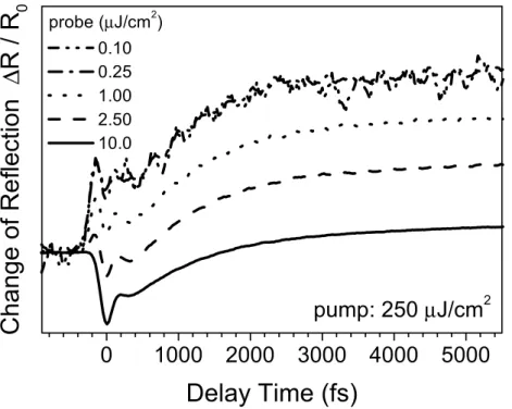
Figure 3.4 Differential reflectivity measurements for a pump fluence of 250 µJ/cm2 with the probe flu-ence varied as indicated.
0
1000 2000 3000 4000 5000
probe (µJ/cm2) 0.10 0.25 1.00 2.50 10.0pump: 250
µJ/cm
2Change of Re
flection
∆
R /
R
0Delay Time (fs)
signal-to-noise ratio degraded. However the qualitative change from bleaching to induced absorption is clearly observed as the probe power is varied. Depending on the operating wavelength, the fluence of the probe required to eliminate bleaching effects varies. At suffi-ciently high fluences the probe pulse alone bleaches the available states. Excitation by the pump cannot further increase transmission of the measured probe; it can only decrease the reflection by inducing absorption.
Pump-probe experiments at 1.54 µm with a high probe fluence (80 µJ/cm2, well above Fsat~5 µJ/cm2) were performed on the structure of Figure 2.2 to separate induced absorption dynamics from those due to bleaching by state filling. Figure 3.5 compares pump-probe
Figure 3.5 Differential reflectivity measurements at a pump fluence of 320 µJ/cm2 for low (solid curve)
and high (dashed curve) probe fluence, and the difference between the two (dash-dotted curve).