Effect of Metallization on Electrical Performance of Surface Acoustic Wave Resonators
By Jason W. Chu
Submitted to the Department of Electrical Engineering and Computer Sciences
in Partial Fulfillment of the Requirements for the Degrees of
Bachelor of Science in Electrical Engineering
and Master of Engineering in Electrical Engineering and Computer Science
at the Massachusetts Institute of Technology
February 1996
Copyright 1996 Jason W. Chu. All rights reserved.
The author hereby grants to M.I.T. permission to reproduce
and to distribute copies of this thesis document in whole or in part,
and to grant others the right to do so.
Author
Department of Electrical Engineering and Computer Science
February 7, 1996 Certified by_ Carl Thompson--,Thesis Supervisor
Accepted by pF. R. Morgenthaler Chairman, Deprtment Committee on Graduate Theses;J:ASGACG'USET'TS INS !; UIL OF TECHNOLOGY
JUN 1
11996
Eng.
Effect of Metallization on Electrical Performance of Surface Acoustic Wave Resonators
By Jason W. Chu
Submitted to the
Department of Electrical Engineering and Computer Science
February 7, 1996
In Partial Fulfillment of the Requirement for the Degree of Bachelor of Science in Electrical Engineering
and Master of Engineering in Electrical Engineering and Computer Science
ABSTRACT
It was hypothesized that the grain size in metal interdigital transducer (IDT) fingers of surface acoustic wave (SAW) resonators might have a strong influence on the resonator phase noise performance. To determine if this is the case, different IDT metallization processes were employed to alter the grain size in Al and Al-alloy IDT fingers. Grain sizes were varied by changing the ambient 02 pressure during deposition, and the effects of grain sizes were compared with compositional effects through addition of Si and Ti, as well as Cu, in the Al film. The electrical performance of SAW devices were measured; and several samples were analyzed using transmission electron microscopy to determine the corresponding microstructure of metal fingers. It was found that there was no correlation between the average grain size of the IDT fingers and the phase noise performance of the respective SAW resonators.
Thesis Supervisor: Carl V. Thompson Title: Professor of Electronic Materials
ACKNOWLEDGMENTS
I would like to express my appreciation to Dr. Jim Greer for initiating this project and for all the support he has given me through out the duration of this work. I would
also like to thank Prof. Carl Thompson for his guidance and support.
It would not have been possible to finish this project without the help from those at
the Lexington Laboratory of Raytheon Company: Dr. Gary Montress, Donald Andres,
Ernie Sabatino, Brendan Howard, Tom McCullough, Mark Hall, and Steve Fischer. I just
want to say a big "Thank you!"
I want to thank all my friends, who made my five years here the best time of my
life.And finally, I would like to express my greatest gratitude to my parents, without
whose sacrifices, I would not be where I am today.
Table of Contents
LIST OF TABLES... ... 5
LIST OF FIGURES...6
1. INTRODUCTION...8
1.1 SAW resonator frequency stability... ... 1.2 Effect of IDT metalss...9
1.3 Thesis objective...11
2. THEORETICAL BACKGROUND... 18
2.1 Piezoelectric Effect... 18
2.2 Physical Properties of Quartz... 19
2.3 Properties of Al and Cu/Al... ... ... 20
2.3.1 Electromigration... ... ... 20
2.3.2 Stress induced migration... ... 21
2.4 Relevant Work... 21
2.4.1 Effect of impurity doping on gain size...21
2.4.2 "Bur-in" effect...23
2.4.3 Effect of impurity doping on SAW performance... ... 24
3. EXPERIMENTAL METHOD... 36 3.1Device Fabrication...36 3.1.1 Metallization... ... 37 3.1.2 AQP Sealing... ... 38 3.2 Performance measurement... ... 39 3.3 Electron Microscopy... ... 40 4. RESULTS ... 46 4.1 Electrical performance... ... 46 4.1.1 Flicker noise...46 4.1.2 Film resistance... 47
4.1.3 Sealing-induced frequency shifts (SIFS) ... 47
4.2 Microstructure analysis ... ... 47
4.2.1 TEM observations ... 47
4.2.2 SIMS depth profiles... ... 49
5. DISCUSSION...67
5.1 Grain size and SAW noise performance... .. ... 67
5.2 Other electrical performance... 69
6. CONCLUSIONS...76
List of Tables
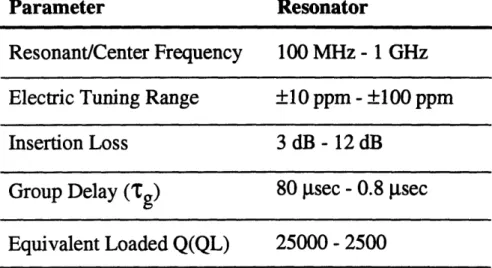
Table 2.1. Typical SAW device electrical parameters.
Table 2.2.1. A summary of SAW properties for several useful cuts of quartz.
Table 4.1. Summary of SAW resonator electrical performance measurement results. Table 4.2.1. The devices and the corresponding average grain sizes and standard
deviations.
Table 4.2.2. The atomic concentration of each element in various metallizations. Table 5.2.1. Sheet resistance of variously doped Al films and the average grain sizes of
List of Figures Fig. Fig. Fig. Fig. Fig. Fig. 1.1.1. 1.1.2. 1.1.3. 2.1. 2.2. 2.1.1. Fig. 2.2.1 Fig. 2.2.2 Fig. 3.1.1. Fig. 3.2.1. Fig. 3.3.1. Fig. 4.1.1. Fig. 4.2.1.1. Fig. 4.2.1.2. Fig. 4.2.1.3. Fig. 4.2.1.4. Fig. 4.2.1.5. Fig. 4.2.1.6. Fig. 4.2.1.7.
Characteristic power law dependence of simple oscillator spectral densities. Fractional frequency change versus temperature for ST-X cut of quartz. Systematic and random contribution to long-term frequency stability. Picture of an all quartz package (AQP) SAW resonator.
Diagram illustrating the all quartz package (AQP).
Method for transforming mechanical energy into electrical energy in a piezoelectric crystal.
Dependency of the change in resonator frequency of quartz on temperature.
Variation of quartz turn-over temperatures with quartz orientation. Design for the two-port resonator used in this study.
The schematics for the resonator phase noise measurement system. Thinned TEM sample before undergoing ion milling.
Resonator phase noise level of a device with Al/Cu IDT metallization, both before and after "burn-in."
A TEM picture of an Al/Cu IDT finger. Pre-burn-in. A TEM picture of an Al/Cu IDT finger. Post-burn-in.
A TEM picture of an IDT finger with Al/Cu deposited in UHV. Post-bum-in.
A TEM picture of an IDT finger with Al/Cu doped with 0.5 atomic percent Si. Pre-burn-in.
A TEM picture of an IDT finger with Al/Cu doped with 3 atomic percent Ti. Pre-burn-in.
A TEM picture of an IDT finger with Al/Cu bled in with 02 under 5x10⁶.
Pre-burn-in.
Fig. 4.2.1.8. Fig. 4.2.2.1.
Fig. 4.2.2.2.
Fig. 4.2.2.3.
Fig. 4.2.2.4.
Typical SAD ring pattern of the devices examined.
SIMS depth profile of Si/Cu doped Al films. (a). Before annealing. (b) After annealing.
SIMS depth profile of Ti/Cu doped Al films. (a) Before annealing. (b) After annealing.
SIMS depth profile of Al/Cu films bled in with 02. (a) Before annealing. (b) After annealing.
Depth profile shows that after annealing, Si concentration goes up in Al/Cu film bled in with 02 under 5x10⁶Torr.
Fig. 5.1.1. SAW oscillator closed-loop phase noise at 1 Hz offset vs. average grain size of IDT fingers.
Fig. 5.1.2. Al/Cu IDT finger grain size distribution. (a). Before "bum-in." (b). After "burn-in."
Fig. 5.2.1. Spread of SIFS vs. average grain size of IDT fingers with various metallization.
1. Introduction
Low noise surface acoustic wave (SAW) oscillators have played an increasingly important role in the field of frequency control during the past twenty years. They not only have been deployed in various military radar and navigation systems, but also have become very popular in areas such as consumer appliances and communication system design [1]. High performance oscillators may be stabilized using SAW resonators fabricated on single-crystal quartz substrates with copper-doped interdigital transducers (IDTs). For high performance military applications, important electrical parameters include residual flicker phase noise level, power handling ability, and long-term frequency shift. Considerable research has been performed to improve these characteristics in order to meet the increasingly rigorous demands of next-generation systems. An improved understanding of potential contributory sources of residual flicker phase noise is the underlying motivation behind this project.
1.1 SAW Resonator Frequency Stability
There are many factors which may influence the electrical performance of SAW resonators, and ultimately oscillators. Some of these factors are described below.
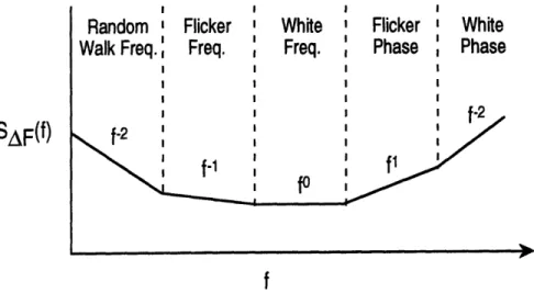
Parker, et al. [2] has shown that the size of the active acoustic area of the resonator has a significant impact on its short-term frequency stability, commonly known as flicker (1/f) noise (Fig. 1.1.1) level. The active acoustic area is the region where over 90% of the device's acoustic energy is concentrated. In separate studies, Parker measured the flicker (1/f) noise levels of more than 60 devices with different acoustic areas [2-5]. He found that the flicker (1/f) noise level is inversely proportional to the active acoustic area of the SAW resonator. He further stated that the observed size dependency is explained by the presence of a large number of independent, localized velocity fluctuations in the quartz.
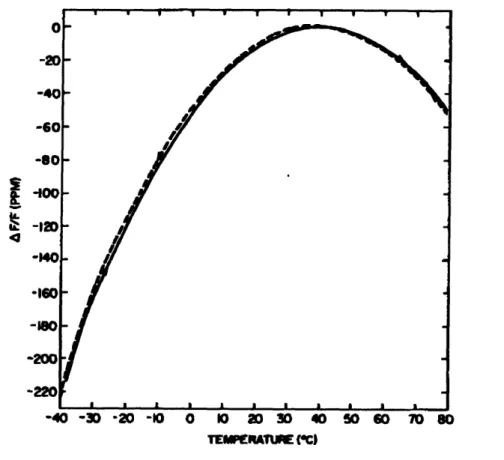
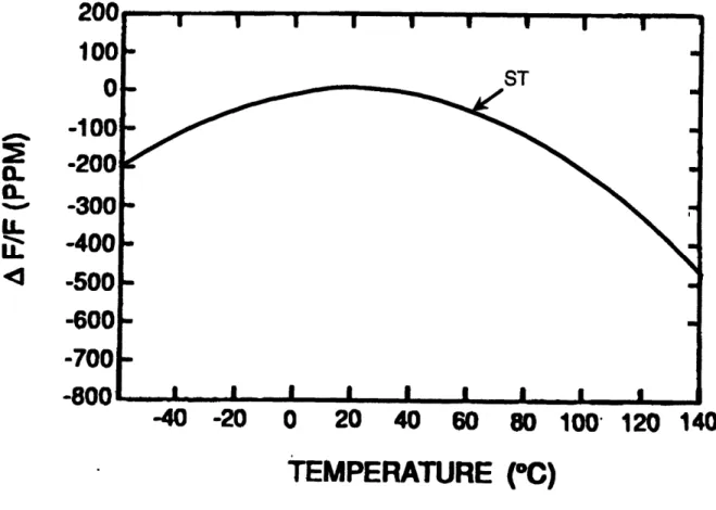
Temperature sensitivity is another factor that influences the resonator's frequency response. A characteristic of an useful resonator is that its resonant frequency does not vary much over a specified temperature range, typically -550C to +1250C. The basic frequency versus temperature characteristic of SAW devices fabricated on ST-X quartz is shown in Figure 1.1.2. The resonant frequency shifts as temperature varies. This relationship can be summarized by the following equation [6],
AF / F = A ( T
-T
0 )2 Eq. 1.1.1where A is the quadratic (second order) temperature coefficient and has an approximate value of -35 x 10-9 / (o C) 2 [6], AF is the shift in frequency, F is the resonant frequency, T is the device temperature, and To is the turn-over temperature.
Aging, or long-term frequency stability, is an important criterion in evaluating high performance oscillators. In general, almost all applications of high performance SAW oscillators require an aging rate of less then ±1 PPM/year [7]. It has been well documented that the resonant frequency of the SAW oscillators always changes after a long period of time (weeks to years) [6-10]. A typical aging diagram is shown in Figure
1.1.3. The cause of this frequency drift is believed to be the relaxation phenomena in or around the SAW device. Stress relaxation in mounting structures or transducer metallization, and adsorption and desorption of foreign materials on the surface of the SAW substrate are common causes for long-term frequency shift. These processes often result in a change of the oscillators' frequency that increases logarithmically with time [6].
1.2 Effect of IDT Metals
The IDTs are usually made out of aluminum doped with a small amount of copper. Aluminum is used due to its excellent acoustic impedance match to quartz. Gold, for example, is not a good choice of metallization for use on quartz, since it leads to devices with excessive insertion loss due to its poor acoustic impedance match. They serve to convert electrical energy to acoustic energy on the piezoelectric substrate. The
typical minimum feature size of the Cu/Al fingers is between 1 and 3 gm wide, and the thickness is between 600 and 1000 A for SAW devices operating in the 300 MHz to one GHz range.
Previous research has indicated that one of the factors affecting the SAW resonator's performance maybe the variations in the microstructure of the IDTs. For example, Bray, et al. observed that SAW devices with ragged metallization had higher residual flicker (1/f) phase noise level [ 11]. Tanski demonstrated in his study that the use of Cr underlayers to enhance adhesion in the metallization process would lead to an increase in the phase noise of 15 dB on average [12]. In a paper published in 1985, Jungerman, et al proposed that "there are noise mechanisms arising from transducer metallizations ...[13]" All of these observations illustrate the potentially significant influence which the IDT's metal may have on SAW resonator performance.
Two pieces of evidence have led to the hypothesis that there may be a direct relationship between the grain size of the metal IDT fingers and the performance of the SAW resonator. The evidence discussed below supports the assertion that larger grains in the IDTs would lead to a reduction in phase noise level.
In a study done in 1985, Loboda, et al. showed that the SAW resonator's noise performance can be significantly improved by operating the device with a high power RF drive signal in the range of +24 to +33 dBm for a period of time after it is packaged. The reduction in phase noise level ranged from 0 to 26 dB in over 40 devices. While he did not know the exact cause of this phenomenon, he hypothesized that this process "caused an annealing-like action to occur in the metal films which comprise the interdigital transducers [14]." It is well known that thermal annealing process increases the metal grain size since grain-growth is a function of temperature [11]; and the stress induced annealing may have yielded larger grain sizes and thus the reduction in the resonators' phase noise level.
The second piece of evidence is the research conducted by Greer, et al. [15] in 1990. He demonstrated that variations in the doping of the IDT metal can have a significant impact on the performance of the SAW resonators. Greer doped either pure Al or Cu/A1 IDTs with small amounts of Ti and/or Si, and found that with the exception of Cu/Al doped with Ti, all other metallizations had greatly degraded the electrical performance of the resonators [15]. Since doping Al or Cu/Al with impurities such as Si or Ti would in general reduce the metal grain size [17-19], one may speculate that the smaller grain size might have led to the degradation in performance.
1.3 Thesis Objective
Even though there is evidence which suggests a potential correlation between the grain size and resonator performance, there has not been any work done directly on this subject. This project is specifically designed to explore the potential influence the grain structure of the IDT fingers may have on the electrical performance of the SAW resonators. Two approaches to modify grain size were implemented. The first was adding small amounts of impurities such as Si and Ti. The second approach was incorporating reactive gases such as 02 in the IDT metallization. By identifying the relationship between phase noise level and IDT metal grain size, we may be able to further refine the IDT finger metallization process in order to improve the resonator's performance.
During this study, different IDT metal compositions are tried. The electrical properties of the devices are measured; and then TEM analysis is performed on selected devices. After the data is gathered, a potential correlation between the samples' phase noise levels and TEM results is sought. The details of the experiment methodology is described in Chapter 3.
References
1. C. C. W. Ruppel, R. Dill, A. Fischerauer, G. Fischerauer, W. Gawlik, J. Machui, F. Muller, L. Reindl, W. Ruile, G. Scholl, I. Schropp, and K.C. Wagner, "SAW Devices for Consumer Communication Applications", IEEE Transactions on Ultrasonics,
Ferroelectrics, and Frequency Control, Vol. 40, No. 5, September 1993, pp. 438-451.
2. T. E. Parker and D. Andres, "l/f Noise in Surface Acoustic Wave (SAW) Resonators", in Proceedings of IEEE Frequency Control Symposium, 1994, pp. 530-538.
3. T. E. Parker and D. Andres, "Dependence of SAW Resonator llf Noise on Device Size", in Proceedings of the IEEE Frequency Control Symposium, 1993, pp. 178-185. 4. T. E. Parker, "Dependence of SAW Resonator 1/f Noise on Device Size", IEEE
Transactions on Ultrasonics, Ferroelectrics, and Frequency Control, Vol. 40, No. 6,
November 1993, pp. 831-833.
5. T. E. Parker, D. Andres, J. A. Greer, and G. K. Montress, "1/f Noise in Etched Groove Surface Acoustic Wave (SAW) Resonators", IEEE Transactions on
Ultrasonics, Ferroeletrics, and Frequency Control, Vol. 41, No. 6, November 1994,
pp. 853-862.
6. T. E. Parker and G. K. Montress, "Precision Surface-Acoustic-Wave (SAW) Oscillators", IEEE Transactions on Ultrasonics, Ferroelectrics, and Frequency
7. G. K. Montress, T. E. Parker, and D. Andres, "Review of SAW Oscillator Performance", in Proceedings of IEEE Ultrasonics Symposium, Vol. 1, 1994, pp. 43-54.
8. G. K. Montress, T. E. Parker, and M. J. Loboda, "Extremely Low Phase Noise SAW Resonator Oscillator Design and Performance", in Proceedings of IEEE Ultrasonics
Symposium, Vol. 1, 1987, pp. 47-52.
9. T. E. Parker and G. K. Montress, "Low Noise SAW Resonator Oscillators", in
Proceedings of IEEE Frequency Control Symposium, 1989, pp. 588-595.
10. T. E. Parker and G. K. Montress, "Frequency Stability of High Performance SAW Oscillators", in Proceedings of the IEEE Ultrasonics Symposium, Vol. 1, 1989, pp. 37-45.
11. R. C. Bray, L. L. Pendergrass, C. A. Johnsen, T. L. Bagwell, and J. L. Henderson, "Annealing behavior and phase noise performance of SAW resonators", in
Proceedings of IEEE Ultrasonics Symposium, Vol. 1, 1985, pp. 247-252.
12. W. J. Tanski, "The influence of a chrome film bonding layer on SAW resonator performance", in Proceedings of the IEEE Ultrasonics Symposium, Vol. 1, 1985, pp. 253-257.
13. R. L. Jungerman, R. L. Baer, and R. C. Bray, "Delay dependence of phase noise in SAW filters", in Proceedings of IEEE Ultrasonics Symposium, Vol. 1, 1985, pp. 258-261.
14. M. J. Loboda, T. E. Parker, J. A. Greer, and G. K. Montress, "Reduction of close-to-carrier phase noise in surface acoustic wave resonators", in Proceedings of IEEE
Ultrasonics Symposium, Vol. 1, 1987, pp. 43-46.
15. J. A. Greer, T. E. Parker, and G. K. Montress, "Metallizations for Surface Acoustic Wave Resonators: Film Properties and Device Characteristics", in Proceedings of the
IEEE Ultrasonics Symposium, Vol. 1, 1990, pp. 483-491.
16. R. E. Reed-Hill, Physical Metallurgy Principles, 2nd ed., PWS-KENT Publishing Company, Boston, 1973, pp. 310-311.
17. L. E. Murr and M. C. Inman, "Effects of vacuum environment on the sub-structure of evaporated F.C.C. metal films", Philosophical Magazine, Vol. 14, No. 27, July, 1966. 18. A. Yuhara, H. Watanabe, N. Hosaka, J. Yamada, and A. Iwama, "Sputter deposition
for high power durable SAW electrode", Japanese Journal ofApplied Physics, Vol. 27, Supplement 27-1, 1988, pp. 172-174.
19. S. R. Wilson, D. Weston, and M. Kottke, "The effects of Si addition on the properties of AlCu films used in multilevel metal systems", in Proceedings of Materials Research
SAF(f)
Random
Walk Freq.
Flicker
Freq.
White
Freq.
Flicker
Phase
White
Phase
f
Fig. 1.1.1. Characteristic power law dependence of simple oscillator spectral densities. Adapted from [6].
f
fo
'•2
-40
-20
0
20
40
60
80 100"
120 140
TEMPERATURE (°C)
Fig. 1.1.2. Fractional frequency change versus temperature for ST-X cut of quartz. Adapted from [6].
2'
1
uu
000O
0
30
O0
)0
)0
0n
0.. CLCL
,%woLL
-1I
-2
-3(
-4(
-5C
-6
-80
I IT I I I I I I-IST I_ 0 LA ( I ( I .I I I 0A r,WEEKS
Fig. 1.1.3. Systematic and random contribution to long-term frequency stability.
2. Theoretical Background
The SAW devices used in this study consist of two IDTs fabricated on a single-crystal substrate as illustrated in Figure 2.1. Some of the typical SAW device parameters are listed in Table 2.1. When an AC voltage is applied to the input transducer, a surface acoustic wave is generated due to the reverse piezoelectric effect. This wave propagates along the quartz surface and sensed by the output transducer which converts this wave into an electrical signal. A two-piece, all-quartz package(AQP) sealing technique is used to package the devices. A figure demonstrating typical AQP SAW resonator packaging is shown in Figure 2.2.
2.1 Piezoelectric Effect
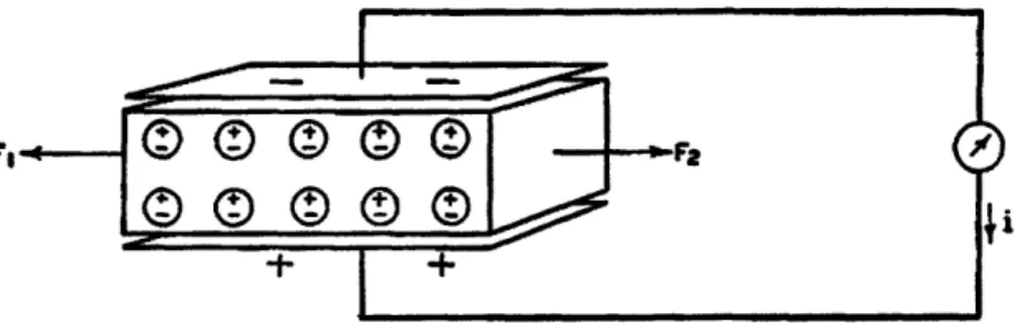
Derived from the Greek word "piezein" or "pressure"-electricity, piezoelectricity was first discovered by Pierre and Jacques Curie more than a hundred years ago. Essentially, the piezoelectric effect is a phenomenon that occurs when a mechanical stress is applied to certain dielectric crystals such as quartz, which results in charge polarization.
When a piezoelectric crystal is not under any outside influence, its positive and negative charges coincide. However, as pressure is applied to the crystal, the charges separate and form a dipole moment in each molecule. A dipole moment is defined as the product of the charge and the distance between the two opposite charges. An electrical field then results from the dipole moment. Figure 2.1.1. demonstrates this transformation from mechanical energy to electrical energy. Conversely, an electrical field can be used to distort the crystal lattice. This is called the reverse piezoelectric effect [1]. The use of piezoelectric crystals in bulk acoustic wave (BAW) and SAW devices has been well developed; and the reverse piezoelectric effect is applied in the design of the SAW resonator devices used in this study.
2.2 Physical Properties of Quartz
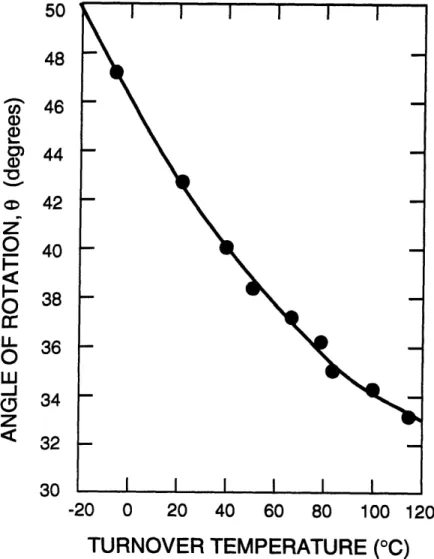
There are many crystalline forms of silica, however, only low temperature quartz, or a-quartz is used extensively in piezoelectric devices. Quartz is a good candidate for SAW devices because of its density and Poisson's ratio are very similar to those of aluminum. However, the most important reason for its wide spread use as a SAW substrate is that its fractional change in frequency, AF/F in PPM/OC is small compared to other materials. This property minimizes the problems associated with large frequency change that comes with using other materials such as lithium niobate. The change in resonator frequency of quartz over temperature is parabolic in nature with a vertex point known as its "turn-over temperature (Fig. 2.2.1)." Around the turn-over temperature, To, the change in frequency with temperature is minimal and the To can be shifted by varying the orientation of the crystal. Figure 2.2.2 shows the dependence of To upon various cut angles [2].
The spacing of the interdigital fingers and the cut of the crystal determines the wave velocity and therefore the resonant frequency of the device. For a particular temperature, the surface wave velocity is a function of the orientation of the crystal. To achieve a desired frequency-temperature characteristics, the substrate of the SAW device is cut at a specific angle with respect to the basal plane of the quartz crystal. The predominant direction of the surface wave propagation is determined by the substrate cut as well. Rayleigh waves are suppressed in the X2 and X3 directions, and thus propagate in the X1 direction. There are other types of surface waves such as Bleustein-Gulyaev, Love wave, shallow bulk acoustic wave (SBAW), etc. These unwanted modes are suppressed by selecting a particular substrate cut. Table 2.2.1 summarizes several important material properties for a useful range of quartz substrate orientations [3-4].
2.3 Properties of Al and AI/Cu
2.3.1 Electromigration
When electric conductors carry high density currents at elevated temperatures, the atoms of the conducting metal or alloy migrate under the influence of the electric field. This mass transport, called electromigration, is normally not uniform along the conductor, and regions of mass buildup and mass depletion are in turn created. Voids grow in size and can lead to metallization failure, most often in the form of an "open circuit" Aluminum is a common metallization material in the integrated circuit industry, and is subject to this problem. Since the first observations in microelectronic devices made by Blech, et al. [5], void and hillock formation due to electromigration have been the topics of much study. Electromigration in pure Al interconnects is caused by the interaction between conducting electrons and the conductor atoms. A net flux of atoms in the direction of current flow results from this interaction. This flux of atoms, J can be expressed by eq. 2.3.1.1 [5]
ND J = ND Z*epj
kT Eq. 2.3.1.1
where N is the atomic density, D is the diffusivity, Z*e is the effective charge of the metal ions, p is the resistivity of the conductor, j is the current density, k is Boltzmann's constant and T is the absolute temperature. It has been possible to overcome many of the shortcomings of aluminum as a metallization for integrated circuits through the addition of other components. The addition of copper to aluminum has resulted in alloy metallization with greatly improved electromigration resistance [6-7]. The copper segregates to the grain boundaries, causing a reduction of aluminum diffusivity along the grain boundaries, which lessens the migration rate.
2.3.2 Stress induced migration
SAW resonators fabricated with pure aluminum transducers showed the formation of dendrite-like growths and a degraded electrical response after a relatively short
operating time at high power levels [8]. Voiding was also present in SAW devices. It was
initially speculated that this was caused by electromigration. Later, it was discovered that this was due to stress-induced material migration [8-9]. In a series of experiments conducted by Shreve, et al. [9], aluminum metallization was placed within the acoustic aperture so that it was exposed to the acoustic energy, but was grounded to eliminate current flow. It was found that the aluminum migration corresponded to the peak displacement of the surface acoustic wave and that there existed a direct correlation between higher acoustic energies and increased voiding of the metallization.It was found that adding a small amount of Cu to the Al film would reduce or eliminate these migration effects. In a study done in 1979, Latham, et al. [8] showed that resonator devices fabricated with 2% Cu doped Al film resulted in up to 65 times greater lifetime. The observation that the addition of Cu improves the performance of SAW resonators has been echoed by many studies [8-15]; and currently Al/Cu is the standard
metallization in SAW production for military applications.
2.4 Relevant Work
2.4.1 Effect of impurity doping on grain size
Certain impurity doping can retard the parent metal grain growth [16]. When impurity atoms are introduced, an elastic stress field is formed if the size of the foreign atom is different from that of the parent atom. This induces a strain energy which can be lowered if the atom segregates to the grain boundaries, which can result in a drag force which can suppress grain boundary motion and grain growth.
The effect of different foreign elements on the parent material grain growth varies. It is suggested that the difference is caused by the variation in strain magnitude produced
by different elements. Those elements which generate the greatest distortion in the lattice structure may have the largest impact on the grain growth. It has been shown that the injection of even 0.01% oxygen in copper can significantly reduce the grain size of copper [16].
Murr, et al. [17] showed that the background vacuum pressure during the metal deposition process plays a role in determining grain size as well. Al with 99.9999% purity was vapor deposited on a NaCl substrate. Background pressure levels of 2x10², 2x10"5, and 2x10"9 Torr were used. The approximate film thicknesses were 1400 A, 1500
A,
and 2000A,
respectively. Substrate temperature was kept at 4250C; and the deposition rate was about 1000 A/sec. It was observed that the average grain size increased as the evaporation pressure was reduced, indicating that the higher amount of impurities that were allowed in the lower pressure environment might have hindered the Al grain growth.Wilson, et al. [18] saw a reduction in metal grain size when doped with Si. In this case, Al films doped with Cu and/or Si were sputter deposited on oxidized Si wafers. The deposition rate was approximately 1.1 im/min. They found that the average grain size increased with the deposition temperature, and that Si clearly reduces both the average grain size and the range of the grain size at the deposition temperature of 4350C. At that temperature, the Al film doped with 0.5% Cu had an average grain size of 4.5 gm, while the average grain size of the Al film with the same concentration of Cu, but with 0.5% Si, was 2.8 gim.
While testing the power handling ability of the SAW resonator devices with sputtered Al film IDTs, Yuhara, et al. [19] noticed that a reduction in grain size occurred in the films doped with Ti. The deposited film thickness was 1000 A; and the substrate temperature during the deposition process was 2000C. It was observed that the grain size decreased as the concentration of the Ti increased. The approximate grain size of the sputtered Al film with no Ti was about 0.08 gim, and it was ultimately reduced to 0.06 jim
with the injection of Ti with a weight concentration of 0.6 %, 0.05 gm with 0.9 % Ti, and 0.04 pm with 2.1 % Ti.
2.4.2 "Bum-in" effect
Loboda, et al. [20] discovered that close-to-carrier phase noise in SAW resonator devices can be greatly reduced by the "burn-in" process. "Burning-in" a device is carried out by operating it with a higher than normal incident RF power level for a period time, at a frequency corresponding to the devices' resonant frequency.
The SAW resonator devices used in their study were 350 to 810 MHz two-port resonators fabricated on single-crystal quartz with either Al or Cu/Al IDTs. The thickness of the metal IDTs ranged from 1 to 1.5 gm. A Hewlett-Packard 11740A Phase Noise Measurement System in an open-loop mode was used to measure the devices' phase noise. After the initial noise measurement, those devices went through the "burn-in" process, and were measured again for their post "burn-in" noise level. The RF power level used in "bum-in" ranged from +24 to +33 dBm; and the time duration varied from
several minutes to hours.
Loboda, et al. [20] found that the phase noise levels of the devices that went through "burn-in" were lowered by an average of 8 dB; and the time required was approximately an hour. Some resonators also exhibited a small reduction in the ohmic resistance of their transducer fingers. The peak stress levels during "burn-in" were calculated to be between 1x10W and 4x10⁸- Nt/m2, depending on the devices' acoustic area
and the incident power.
Scanning Electron Microscopy (SEM) was performed on several "burned-in" devices in an attempt to understand the cause for the reduction in noise levels. However,
no observable changes were found.
Several experiments were conducted to separate the effect of high current level and high stress level. To isolate the effect of high current level, an off-resonance
frequency was found where the input impedance was similar to that at the resonance frequency. Then the device was driven by a high power RF signal at that off-resonance frequency, producing the same peak RF current level, but without the stress. The result showed that there was no noise reduction, indicating current level was not a cause for the "bum-in" effect.
To simulate the high stress level without the accompanying current, Loboda, et al. [20] exposed another device to both high and low temperatures by baking it overnight at 3500C and then submersing it in liquid nitrogen (-1960C) for 2 hours. The mismatch of the thermal expansion coefficients between the IDT metal and the quartz substrate induced a high stress level on the device. Phase noise level was measured after both baking and nitrogen cooling. Still, no noise reduction was noticed, implying that stress alone was not responsible for "burn-in" either.
In conclusion, Loboda, et al. [20] suggested that "the bum-in process causes an annealing-like action to occur in the metal films which comprise the interdigital transducers," implying that "burn-in" somehow altered the grain structure of the IDT metals in the same fashion as an annealing process would, which is to induce grain growth. However, he could not provide any concrete evidence. The only thing conclusive from his experiments was that the "bum-in" process definitely improved the flicker (1/f) noise performance of the SAW resonators. Several later studies concurred with this finding [10-12, 14-15].
2.4.3 Effect of impurity doping on SAW performance
In a 1990 study, Greer, et al. [10] evaluated the effect of doping pure Al or Al/Cu transducers with small amount of either Si or Ti. Over 50 two-port AQP SAW resonator devices with various metallizations were used in this study. The devices' resonant frequencies ranged from 300 to 600 MHz; and the thicknesses of their IDT fingers were
between 600 to 900
A.
Electron-beam evaporation in a cryo-pumped vacuum chamber with a base pressure of 2x10⁻⁷ Torr was used to deposit the metal films.Their results showed that doping the IDTs with only Cu or a combination of Cu and Ti would result in good device noise performance. However, devices with IDTs doped with only Ti or Si had very erratic noise levels. The "bum-in" process did not prove to be of much use for those devices doped with either Ti or Si. In certain devices, the flicker (1/f) noise level actually went up after "bum-in". The authors did not provide an explanation for the observed phenomenon.
References
1. R. A. Heising, Ouartz crystals for electrical circuits: their design and manufacture, third printing, D. Van Nostrand Company, Inc., New York, 1952, pp. 16-19.
2. J. F. Dias, H. E. Karrer, J. A. Kusters, J. H. Matsinger, and M. B. Schulz, '"he temperature coefficient of delay-time for x-propagating acoustic surface-waves on rotated Y-cuts of alpha quartz", IEEE Transaction of Sonics Ultrasonics, Vol. SU-22, No. 1, January 1975, pp. 46-50.
3. T. E. Parker and G. K. Montress, "Precision Surface-Acoustic-Wave (SAW) Oscillators", IEEE Transactions on Ultrasonics, Ferroelectrics, and Frequency
Control, Vol. 35, No. 3, May 1988, pp. 342-364.
4. T.E. Parker and D. Lee, "Stability of phase shift on quartz SAW devices", in
Proceedings of IEEE Frequency Control Symposium, 1979, pp. 379-387.
5. I. A. Blech and H. Sello, Physics of failure in Electronics, Ch. 5, 1966, pp. 496.
6. I. Ames, F. M. d'Heurle, and R.E. Horstmann, IBM Journal of Research and
Development, 1970, pp. 461.
7. A. J. Learn, "Aluminum alloy film deposition and characterization", Thin Solid Films, 20, 1974, pp. 261-279.
8. J. I. Latham, W. R. Shreve, N. J. Tolar and P .B. Ghate, "Improved Metallization for Surface Acoustic Wave Devices", Thin Solid Films, 64, 1979, pp. 9-15.
9. W. R. Shreve, R. C. Bray, S. Elliot, and Y. C. Chu, in Proceedings of IEEE
10. J. A. Greer, T. E. Parker, and G. K. Montress, "Metallizations for Surface Acoustic Wave Resonators: Film Properties and Device Characteristics", in Proceedings of the
IEEE Ultrasonics Symposium, Vol. 1, 1990, pp. 483-491.
11. T. E. Parker and G. K. Montress, "Precision Surface-Acoustic-Wave (SAW) Oscillators", IEEE Transactions on Ultrasonics, Ferroelectrics, and Frequency
Control, Vol. 35, No. 3, May 1988, pp. 342-364.
12. G. K. Montress, T. E. Parker, and D. Andres, "Review of SAW Oscillator Performance", in Proceedings of IEEE Ultrasonics Symposium, Vol. 1, 1994, pp. 43-54.
13. G. K. Montress, T. E. Parker, and M. J. Loboda, "Extremely Low Phase Noise SAW Resonator Oscillator Design and Performance", in Proceedings of IEEE Ultrasonics
Symposium, Vol. 1, 1987, pp. 47-52.
14. T. E. Parker and G. K. Montress, "Low Noise SAW Resonator Oscillators", in
Proceedings of IEEE Frequency Control Symposium, 1989, pp. 588-595.
15. T. E. Parker and G. K. Montress, "Frequency Stability of High Performance SAW Oscillators", in Proceedings of the IEEE Ultrasonics Symposium, Vol. 1, 1989, pp. 37-45.
16. R. E. Reed-Hill, Physical Metallurgy Principles, 2nd ed., PWS-KENT Publishing Company, Boston, 1973, pp. 310-311.
17. L. E. Murr and M. C. Inman, "Effects of vacuum environment on the sub-structure of evaporated F.C.C. metal films", Philosophical Magazine, Vol. 14, No. 27, July, 1966.
18. S. R. Wilson, D. Weston, and M. Kottke, "'The effects of Si addition on the properties of A1Cu films used in multilevel metal systems", in Proceedings ofMaterials Research
Society Symposium, Vol. 181, 1990, pp. 545.
19. A. Yuhara, H. Watanabe, N. Hosaka, J. Yamada, and A. Iwama, "Sputter deposition for high power durable SAW electrode", Japanese Journal of Applied Physics, Vol. 27, Supplement 27-1, 1988, pp. 172-174.
20. M. J. Loboda, T. E. Parker, J. A. Greer, and G. K. Montress, "Reduction of close-to-carrier phase noise in surface acoustic wave resonators", in Proceedings of IEEE
Parameter
Resonant/Center Frequency
Electric Tuning Range
Insertion Loss
Group Delay (tg)
Equivalent Loaded Q(QL)
Resonator
100 MHz - 1 GHz
±10
ppm - ±100 ppm
3 dB - 12 dB
80
gsec
-
0.8
psec
25000 - 2500
Table 2.2.1. A summary of SAW properties for several useful cuts of quartz. Adapted from [3-4].
Cut Angles Free Surface Metallized Surface Coupling Turnover Time Average (degrees) Velocity Velocity Coefficient Temperature Power Flow Angle
0
o
V (m/s) (m/s) k (OC) (degrees) 0 42.75 0 3158.8 3157.0 0.00116 21 0 0 38.0 0 3154.3 3152.3 0.00125 56 0 0 35.0 0 3152.0 3149.9 0.00129 84 0 0 32.0 0 3150.1 3148.0 0.00134 132 0 0 0 0 3160.5 3157.6 0.00185 N/A 0Fig. 2.1. Picture of an all quartz package (AQP) SAW resonator. Adapted from [3].
PBN-90-0752C
Matching Quartz Cover
1_-.002" SAW Substrate SAW Device
(a)
CoverN
4
Glass Frit(b)
Fig. 2.2. Diagram illustrating the all quartz package (AQP). Adapted from [3].
Glass Frit Notch Cut Into Cover Substrate
V
L
6or
II IIflUflOhll
III[JOO[J
Exposed Bonding Pads2
I\I
•11 1 1~1~~1~~ J•JJJ•J JJISSIIlfIIIICI-IfS rlJJJ•J •Sfff·fI
FtJ"c~c~
I
|I
91
Fig. 2.1.1. Method for transforming mechanical energy into electrical energy in a piezoelectric crystal. Adapted from [1].
0 -20 -40 -60 -80 S-12D o-s *160
-220
-40 -30 20 -0 0 10 20 30 40 50 60 70 80 TEWIRAToRE (fC)0 O0
O
!-U-O
w
-Jz"
48 46 44 42 40 38 36 34 32 30 -20 0 20 40 60 80 100 120TURNOVER TEMPERATURE (oC)
Fig. 2.2.2 Variation of quartz turn-over temperatures with quartz orientation. Adapted from [2].
3. Experimental Method
SAW resonator devices with various IDT metal compositions were fabricated by the Raytheon SAW group at the Lexington Laboratory. Their electrical properties were measured, and about half of them went through the "bum-in" process. The power level used in the "bum-in" process was +30 dBm. TEM analysis was performed on five devices with Al/Cu IDTs, one device with Al/Cu IDT deposited in an ultra high vacuum environment, and one device each with standard Al/Cu doped with either Si, Ti, or 02. Two of the devices with Al/Cu IDTs had been burned-in. The average grain size of each of those devices was calculated, and its association with respective electrical performance was sought.
3.1 Device Fabrication
The two-port SAW resonator devices used in the study were hermetically sealed in all quartz packages (AQPs) using 36.70 rotated Y-cut PQ/PZ quartz substrates and covers. The devices are specifically designed to allow metal to play a role in phase noise performance. The basic layout of the resonator is shown in Figure 3.1.1. The designed center frequency was nominally 450 MHz. Standard photolithography processing was used in the fabrication process. The thickness of the doped Al film ranged from 700
A
to 800A,
depending on the impurity doping. The metal was deposited using electron-beam evaporation in a cryo-pumped vacuum chamber. The chamber's base pressure was 2x10⁻⁷during deposition. The substrate temperature during the deposition process was near room temperature.
The photomask used in fabrication makes 15 devices per substrate, and two substrates were fabricated per processing run. Sample witness plates were made simultaneously so that blanket films could be obtained for both resistance and SIMS analysis. All of the SAW device fabrications were performed at Raytheon.
3.1.1 Metallization
Different metallizations for the IDTs were tried. The first two were pure Al and Cu doped Al, since they are the standard materials for IDT metallization on quartz substrate. The pressure under which the metal was deposited was approximately 1x10⁻⁶ Tort (predominantly H2 gas). The third batch of devices was Cu doped Al deposited in ultra high vacuum (UHV) with a corresponding background pressure of 6x10⁻⁹ Torr. Other experiments included bleeding in 02 under various pressures during the deposition of the IDTs, and alternatively doping the IDTs with Ti or Si with thickness ranging from 5 A to 30
A.
It was expected that doping with 02, Si, and Ti would reduce the IDT metal grain size [1-4], and that this reduction in grain size would lead to increased flicker (1/f) noise levels of the corresponding SAW resonator devices, as predicated by the hypothesis of this project. The pressure levels used while bleeding in 02 were 3x10U, 5x10,7.5x10-6, and 1x10⁻⁵ Torr.
For the pure Al and Al/Cu metallizations, Al(99.9995%) or 4.5% (by weight) Cu doped Al (99.9995% purity) were used as standard evaporation charge. Charges were
melted using the electron-beam before deposition. After a deposition rate of 10 A/sec was reached by adjusting the temperature, a shutter was opened, exposing the patterned SAW substrates to the evaporant.
When Ti or Si was introduced, a two layer evaporation technique was used. A thin layer of Ti or Si was first electron beam evaporated at a rate of 1 A/sec to a certain thickness. Then without breaking vacuum, 4.5% Cu doped Al was evaporated at 10 A/sec to the desired IDT thickness.
* 1 hour @ ~3600C and -15 minutes @ 425"C
3.1.2 AQP Sealing
The as-fabricated (unsealed) center frequency and insertion loss (IL) of the resonator devices were measured after an oxygen plasma/UV ozone cleaning. Each device was then hermetically sealed in high vacuum (< 10-7 Torr) to matching quartz
covers using a glass frit, thus forming the AQP. During the sealing process, the devices
Material Pressure (Torr) Temperature
Al/Cu 1E-6 Standard Seal Cycle* Pure Al 1E-6 Standard Seal Cycle* Al/Cu 6E-9 Standard Seal Cycle*
A1/Cu bleed in 02 Standard Seal Cycle*
AI/Cu doped with Ti/Si Standard Seal Cycle*
were exposed to a high temperature (>>3600C) anneal for about an hour. The temperature was then raised to melt the glass. The temperature rise usually took about 15 minutes. The devices were slowly cooled down in the furnace. After sealing, the center frequency and insertion loss (IL) were again measured. Sealing induced frequency shifts
(SIFS) were calculated by using eq. 3.1.1. AF
SIFS= A.
Eq. 3.1.1
Fo
where AF is the difference between pre-seal and post-seal frequencies, and Fo is the
reference frequency, which in this case is 449.7 MHz, the nominal center frequency.
3.2 Performance Measurement
The SAW devices were mounted onto a test fixture before undergoing any measurement. The device was adhered to the fixture, and electrical contacts were established using 0.003 in. gold wire which was resistance welded. Each device was characterized on a HP network analyzer for center frequency, IL, and loaded- and unloaded-Q values. Then the device was put in an oven to be thermally stabilized at its nominal operating temperature, which is 650C for all the devices used in this study. An
HP 3048A Phase Noise Analyzer System was then used to measure the open-loop residual phase noise. This is the standard test set-up used for SAW resonator device residual phase noise measurements. A block diagram for the measurement set-up is shown in Figure 3.2.1.
After the open-loop phase noise levels were measured for each device, the equivalent oscillators' closed-loop phase noise levels at a 1 Hz intercept were calculated using equation 3.2.1 [5].
£o(fm) = £R(fm) + 20 x log {(Fo2QL) + 20 x log ({ 1/fm) Eq. 3.2.1 where £o is the oscillator flicker (1/f) noise, £R is the resonator device flicker (1/f) noise, Fo is the carrier frequency, QL is the loaded-Q, and fM is the carrier offset frequency where the noise is compared among all the devices; and in this calculation fM is set to be 1 Hz.
Roughly half of the devices went through the bum-in process after the initial measurement. They were exposed to a power level of +30 dBm for one hour. The stress level induced by such power level is calculated to be approximately 3.5x10"8 N/m2. The
open-loop noise level was again characterized using the same measurement system after "bum-in".
3.3 Electron Microscopy
Transmission Electron Microscopy (TEM) was used to study the microstructure of the IDT fingers. A "back-thinning" technique was used to remove the quartz substrate beneath the IDTs in order to expose the metal film. The middle section of the device was first cut out in a 2x2 mm square with the transducer at the center. The sample was then thinned to approximately -50p.m using a grinder. Afterwards, a copper ring with a radius of 1.5 mm was bonded to the thinned sample using 5 minute epoxy to strengthen the sample and ease handling. Figure 3.3.1 shows a sample bonded with a copper ring. The sample was further thinned by using a Gatan ion-mill. The milling process was carried out
in a liquid nitrogen cooling environment to prevent thermally induced artifacts. The ion beam was set to an angle of 20 degrees with respect to the substrate (sample) normal, with the ion gun operating at 6 kV and 0.5 mA. It usually took about 12 to 15 hours of milling time to reduce the sample to the desired thickness.
A JOEL 200X transmission electron microscope was used to study the grain structure of the IDT fingers. The operating potential of the microscope was set to 200 kV.
References
1. R. E. Reed-Hill, Physical Metallurgy Principles, 2nd ed., PWS-KENT Publishing Company, Boston, 1973, pp. 310-311.
2. L. E. Murr and M. C. Inman, "Effects of vacuum environment on the sub-structure of evaporated F.C.C. metal films", Philosophical Magazine, Vol. 14, No. 27, July, 1966. 3. S. R. Wilson, D. Weston, and M. Kottke, "The effects of Si addition on the properties
of AlCu films used in multilevel metal systems", in Proceedings of Materials Research
Society Symposium, Vol. 181, 1990, pp. 545.
4. A. Yuhara, H. Watanabe, N. Hosaka, J. Yamada, and A. Iwama, "Sputter deposition for high power durable SAW electrode", Japanese Journal of Applied Physics, Vol. 27, Supplement 27-1, 1988, pp. 172-174.
5. T.E. Parker and G.K. Montress, "Introduction to high stability SAW oscillators: Design and performance", Tutorial presented at 1995 IEEE Frequency Control
'0r \ , ° L. M ) •O O U-U t_-ccc i I.-. C7.. .C *, Lr)
II
I 0 1O 0 C In U,m•
UE Ci 7=
CO0 0 0 0 ~t---o~ss----*l vl a) v V1 · h cci Cre ! ImE
+-D
uIE cvEMr cE +-D co E •- CD co E + -0 U, Cd U, 4--Cdcl
0 45,o U, 0 0 edO 00.6-Fingers
50 gm
4. Results
Information for ten batches of SAW resonator devices fabricated using different IDT metallizations is shown summarized in Table 4.1. Included in the Table are the batch identification number, Oscillator phase noise level (£o) and resonator phase noise level (ER) at the one Hz intercept before and after "burn-in", average £o(1 Hz) and standard deviation for each batch, sealing induced frequency shifts (SIFS), and loaded Q (QL). The center frequency for all the devices is nominally 450 MHz, and the power used for bum-in is +30 dBm.
4.1 Electrical performance
4.1.1 Flicker noise
There is no significant difference in phase noise levels among devices with various metallizations; and the noise levels all dropped down to the measurement floor level of
-145 dBc/Hz after "bum-in." Before "bum-in", devices doped with Si, Ti, or 02 appear to have better noise performance. However, whether this improvement is real is debatable due to the +2 dB margin of error of the measurement equipment. The only thing which can be stated conclusively is that all the devices that underwent testing demonstrated excellent flicker noise performance, and that "bum-in" definitely reduced the average flicker (1/f) noise level. Fig. 4.1.1 shows the residual flicker noise level of a device with AI/Cu IDT, both before and after "bum-in." The shape of the noise curves shown is typical of all the devices studied in this work.
4.1.2 Film resistance
The sheet resistance of the variously doped Al films are shown in Table 4.1, both before and after the films had gone through the AQP sealing process. The data was obtained from the quartz witness plates as explained in Chapter 3, section 1. With the exception of the Cu/Ti doped Al film, all films showed a reduction in resistance, some by as much as 30%, after sealing as the result of the high temperature anneal. The Cu/Ti doped Al film had an increase of about 17% in resistance after sealing.
4.1.3 Sealing-induced Frequency Shifts (SIFS)
There is no significant variations among the spread of SIFSs for the various metallizations. The average SIFS for devices fabricated with Cu doped Al IDT evaporated in ultra-high vacuum is 72.9 ± 12 PPM, while that of Al/Cu devices deposited in standard vacuum environment is 48.6 ± 14 PPM. The devices with 02 bled in have the lowest SIFSs (26.3 ± 14 PPM). The average SIFSs for each batch of devices is shown in Table 4.1.
4.2 Microstructure analysis
4.2.1 TEM observations
As expected, there is a great variation in the grain sizes of IDTs with different metallizations. Shown in Figures 4.2.1.1-4.2.1.6 are TEM photos of those IDTs. Among the devices that were not "burned-in", the average grain size of these three devices (Q3943-A2, Q3943-B3, and Q3944-C1) with Al/Cu was 0.22 pm, while that of the device
(Q3948-D2) with Al/Cu doped with one atomic percent Si was 0.19 pm. Devices doped with Ti and with 02 bled in had much smaller grain sizes, almost half that found in Al/Cu IDTs. The sample (Q4034-C3) with three atomic percent Ti had an average grain size of 0.1 pm; and the grain size of the device (Q4033-C1) with 02 bled-in under a background pressure of 5x10 6 was 0.09 pm.
The "bum-in" process did not appear to have increased the grain size. The average grain size for the two pieces (Q3943-E3 and Q3944-A2) with Al/Cu IDTs that have gone through "bum-in" had an average grain size of 0.24 pm. The difference between this and that of Al/Cu devices that were not "burned-in" is statistically insignificant. The third device that had been "burned-in", a piece (Q3939-A2) with Al/Cu IDTs deposited in ultra-high vacuum (6x10⁻⁹), had 0.18 pm as its average grain size. The devices and the corresponding average grain sizes and standard deviations are shown in Table 4.2.1.
Precipitates appeared to be present in some of the films (Fig. 4.1.2.7). The size of the "precipitates" was on the order of the film thickness. Further TEM analysis is required to determine the exact nature of these particles.
SAD ring patterns of those nine samples were analyzed, and no particular preferred orientation was noticed. All of the lower index rings were present in all samples. A typical ring pattern is shown in Fig. 4.2.1.8.
4.2.2 SIMS depth profiles
SIMS analysis was performed on bulk films with various metallizations to obtain quantified material depth profiles. The atomic concentration of each material is calculated from the profiles, and is listed in Table 4.2.2.
Figures 4.2.2.1 (a) and (b) show profiles for Si/Cu doped Al films both before and after annealing. It needs to be clarified that the signal measured at atomic number 29 in Fig. 4.2.2.1 (a), labeled as AIH, is actually an artifact of the analysis technique. The atomic number of both 28Si and the molecule AMH is 28. To avoid confusion, the 29Si
isotope was monitored during the analysis. Depth profiles of Ti/Cu doped Al films, before and after annealing, are shown in Figures 4.2.2.2 (a) and (b). Again the A1H signal shows up in the pre-annealing profile, and its presence is more pronounced due to that fact that Ti is a hydrogen "pump." Until the film substrate is reached, Ti or Si is not present in the bulk of the film. It's evident that Si or Ti diffused into the bulk of the film after the annealing cycle. The corresponding atomic concentration resulted from different metallizations is listed in Table 4.2. One interesting observation is that Si levels went up in a step like fashion in the profiles of the post-annealing Si doped films, as shown in Fig. 4.2.2.1 (b).
Oxygen levels of Al/Cu films with 02 bled in under the various levels of background pressure are shown in Figures 4.2.2.3 (a) and (b), both before and after annealing. The oxygen concentration went down as the pressure level decreased. One unusual finding is that the Si level shot up after annealing in the film with 02 bled-in under
02 under other pressure levels tried in this study. A possible explanation for this observation is that the growth of Al grains is hindered by the addition of excess 02; and this allows more Si atoms to migrate into the bulk of the film. At a higher pressure level such as 1x10 5 Torr, too much 02 goes into the bulk of the film, leaving no space for Si; and at a lower pressure level (3x10-), there is not enough 02 in the film to reduce the
grain size to a level that allows migration of excess Si.
The Cu concentrate was about 0.5 atomic percent in all films, and was not changed by the annealing process. Its distribution throughout the depth of the film was also uniform.
In general, the SIMS depth profiles confirmed that the concentration of each type of impurities was as designed. The concentration levels of Si and Ti (Table 4.2) increased as the deposited layer became thick; and more 02 was allowed at higher pressure levels.
Batch ID Device X Before After S(f) Before S(f) After ID Bum-In Bum-In Bum-In Bum-In
Q-3939 B1 780820 -142 -142 -5281 -52 81 84 5007783
AVCu UHV 2 757685 -143 -144 -5355 -5455 6226373138
Ave Sf)Before BI -51 65. sd 3 43 C2 740872 -145 -145 -5535 -5 35 95.61930176 Ave S 1AfterBI -5452,std 121 C3 747063 -145 -5542 82.2770736
Ave SFS 74 77, std 1152 D1 7348 11 -140 -5028 6448743607
Restance beforelafter anneakng 0 123/0 11 D2 744315 -140 -145 -50 39 -5539 6893484545
03 750837 -140 -5047 71 15855014 El 7076.23 -15 -4495 6 93484545 0-3940 AVCu UHV A2 727963 -137 .4720 35.57927507 Ave S(f)BeforeBI -5386,std 320 B3 776320 -145 -5576 73 38225484 Ave S(f)AfterBI -5522.sld 051 C1 774254 -145 -5573 71.15855014 Ave SIFS 66/43 std 13 47 D1 758484 -145 -144 -55 56 -54 56 73.38225444
Resstance before/atter annealng 0 123Y0 11 D2 7629 05 -140 -145 -5061 -5561 60 04002668
03 765859 -145 -145 -5564 -5564 68.93484545
El 717132 -145 -145 -55 07 -5507 77.82966422
E2 739602 -145 -5534 7115855014
0-3939
AVCu UHV Al 771921 -144 -145 -54 71 -5571 7782966422
Ave S(i) BeforeBI -50 22, std 361 A2 782104 -135 -145 -4582 -5582 82.2770736
Ave S(f)AfterBl -5576.std 008 A3 781625 -144 -5482 845007783
Ave SIFS 78 15, std 8 06 B3 804949 -135 -4607 845007783 Resstance before/after anneabng 0 12310 11 Cl 719664 -140 -50 10 82.2770736
E2 733207 -140 -5026 6226373138 E3 691238 -140 -4975 7338225484 0-3943 AYCu Al 743281 -138 -4838 80 05336891 Ave.S(f)BeforeBI -51 18,std 305 A2 826467 -143 -5430 55.5926173 Ave S(f)AfterBI -55 81,sd 0 19 83 763228 -136 .4661 5114520792 Ave SIFS 54 20, std 17 26 C1 802552 -137 -145 -4805 -56 05 40 02"68446 Resstance beforelafler anneakng 0 155(0 129 C3 788903 -143 -5390 57 81632199
D2 7751 96 -143 -145 -5374 -5574 28 908161
03 7851 44 -142 -145 -5286 -5 86 4447409384
E3 763051 -141 -145 -51 61 -561 7560595953
0-3944
AVCu A2 7281 72 -135 -145 -4520 -5520 4447409384
Ave S(f)Before B -4721,std 193 A3' 622298 -140 -145 .4884 -5384 46.69779653
Ave S(f After BI -5498,std 078 B1 755803 -135 -145 .4552 -5552 40 02668446 Ave SIFS 43 08, std 6 92 82 742351 -140 -145 -5037 -5537 53.36891261
Resstance before/after annealing 0 15510 129 C1 7671 32 -138 -4865 28 908161
C3 7581 55 -135 -4555 44 47409384 D1 7951 98 -135 -4597 44 47409384 03 7628 95 -137 -4761 42.25038915 0-4034 B1 7045 15 -142 -142 -51 91 -51 91 5336891261 AVCurTI. 3 atm % Ti B2 680226 -141 -50 35 57.81632199 Ave S(fBeforeB 56257, std 1 46 C1 714019 -144 -5403 6004002668 Ave S After BI -51 97, sld 0 07 C3 68.93484545 Ave SIfS 6171, std 10 21 D1 713069 -142 -142 -5202 -5202 6004002668
Resistance before/after annealing 0 158/0 185 02 705526 -143 -5293 62.26373138
03 48 92150322 E3 728421 -144 -5420 82.2770736 0-3948 Al 7765 44 -145 -5576 5336891261 AVCa/SI, 0 5 atm. % Si A3 740000 -145 -141 -5534 -54 34 33.35557038 Ave S(f) Before 8 1. 54 16, std 2 37 B1 7635 32 -145 -5561 37 80297976 Ave S(AfterBI -54 99,std 057 B2 744890 -145 -145 -5540 -5540 28 908161 Ave SIFS 38 08, std 8 36 B3 736270 -140 -50 30 33 35557038
Resetance before/after annealing 0 161/0 136 C3 740973 -140 -5035 31 13186569
D2 734270 -145 -5527 40 02668446 D3 731740 -145 -145 -55 24 -5524 4669779653
G-4033 A2 762902 -145 -5561 22.2370462
AVCu bled in Oxygen under 5 00e-6 Torr A3 728779 -145 -14Z -5521 -54.21 40 02668446 Ave. S(f)BeforeBI -5449,std 202 82 784005 -144 -5484 15.56593284
Ave S(f)AfterBI -54 31,std 014 B3 7458.92 -140 -144 -5041 -5441 2001334223
Ave SIFS 2724,std 1222 C1 5114520792
Resetance before/atter annealing 0 246/0 167 C3 743000 -145 -5 38 26.6844563
D1 7524 88 -145 -5549 24 46075161
D2 17.78963754
0-4032 A2 7517 87 -143 -14. -5348 -5548 8.894818768
AICu bled in Oxygen under 3 00e-6 Torr A3 6939 68 -145 -54 78 62 26373138
Ave Sl1) Before BI -5458. std 0 86 82 7471 63 -145 -5542 37 80297976 Ave S(AfterBI -55 55, sd 0 10 C1 764022 .143 -145 -5362 -5562 15.56593284
Ave SlFS 23 90.std 18 40 C2 753346 -145 -5550 22.23704692
Resstance before/after annealing 0 202/0 15 C3 767529 -144 -5466 13 34222815
DI 6 671114076
02 24 46075161
0-3953 A2 722852 -141 -5114 24 460T5161
AYCu bled in Oxygen under 1 00e-5 Torr A3 7292 35 -145 -145 -5 21 -5521 2001334223 Ave S(f Before BI -54 18, std 1 41 81 7175 19 -145 -5507 5336891261
Ave S(f) AfterBI -55 13, std 009 83 739219 -144 -5433 24 46075161 Ave SIFS 27 96,std 11 54 C1 714337 -145 -14/ -5503 -5603 2001334223 Resistance before/after annealing 0 296&0 199 C2 736758 -144 -5430 26 6844563
C3 7241 73 -144 -14- -54 15 55 15 266844563

![Table 2.2.1. A summary of SAW properties for several useful cuts of quartz. Adapted from [3-4].](https://thumb-eu.123doks.com/thumbv2/123doknet/14757372.583247/30.918.129.800.453.707/table-summary-saw-properties-useful-cuts-quartz-adapted.webp)
![Fig. 2.1. Picture of an all quartz package (AQP) SAW resonator. Adapted from [3].](https://thumb-eu.123doks.com/thumbv2/123doknet/14757372.583247/31.918.173.705.403.825/fig-picture-quartz-package-aqp-saw-resonator-adapted.webp)
![Fig. 2.2. Diagram illustrating the all quartz package (AQP). Adapted from [3].](https://thumb-eu.123doks.com/thumbv2/123doknet/14757372.583247/32.918.184.745.368.818/fig-diagram-illustrating-quartz-package-aqp-adapted-from.webp)