$Q\FRUUHVSRQGHQFHFRQFHUQLQJWKLVVHUYLFHVKRXOGEHVHQWWRWKHUHSRVLWRU\DGPLQLVWUDWRU WHFKRDWDR#OLVWHVGLIILQSWRXORXVHIU
2SHQ$UFKLYH7RXORXVH$UFKLYH2XYHUWH2$7$2
2$7$2 LV DQ RSHQ DFFHVV UHSRVLWRU\ WKDW FROOHFWV WKH ZRUN RI VRPH 7RXORXVH UHVHDUFKHUVDQGPDNHVLWIUHHO\DYDLODEOHRYHUWKHZHEZKHUHSRVVLEOH
7KLVLVYHUVLRQSXEOLVKHGLQ
7RFLWHWKLVYHUVLRQ
2IILFLDO85/
an author's https://oatao.univ-toulouse.fr/11390
https://doi.org/10.1109/TNS.2008.2005294
Goiffon, Vincent and Magnan, Pierre and Saint-Pé, Olivier and Bernard, Frédéric and Rolland, Guy Total Dose Evaluation of Deep Submicron CMOS Imaging Technology Through Elementary Device and Pixel Array Behavior Analysis. (2008) In: 45th annual IEEE International Nuclear and Space Radiation Effects Conference (NSREC), 14 July 2008 - 18 July 2008 (Tucson, United States).
Total Dose Evaluation of Deep Submicron CMOS Imaging Technology Through Elementary Device and
Pixel Array Behavior Analysis
V. Goiffon, Student Member, IEEE, P. Magnan, Member, IEEE, O. Saint-pé, F. Bernard, and G. Rolland
Abstract—Ionizing radiation effects on CMOS image sensors (CIS) manufactured using a 0.18 m imaging technology are presented through the behavior analysis of elementary structures, such as field oxide FET, gated diodes, photodiodes and MOSFETs.
Oxide characterizations appear necessary to understand ionizing dose effects on devices and then on image sensors. The main degra- dations observed are photodiode dark current increases (caused by a generation current enhancement), minimum size NMOSFET off-state current rises and minimum size PMOSFET radiation induced narrow channel effects. All these effects are attributed to the shallow trench isolation degradation which appears much more sensitive to ionizing radiation than inter layer dielectrics.
Unusual post annealing effects are reported in these thick oxides.
Finally, the consequences on sensor design are discussed thanks to an irradiated pixel array and a comparison with previous work is discussed.
Index Terms—Active pixel sensors (APS), CMOS image sensors (CIS), field oxide FET (FOXFET), gated diode, inter layer dielec- tric FET (ILDFET), ionizing radiation, radiation-hardening-by- design (RHDB), total dose.
I. INTRODUCTION
T
OTAL ionizing dose effects on CMOS image sensors (CIS) for space and scientific applications have been studied [1]–[6] for several years. However, there is a techno- logical gap between older process generations used in previous work and deep submicron technologies (DSM) dedicated to imaging used nowadays. Especially, because of the use of shallow trench isolation (STI) instead of LOCOS and in-pixel dedicated doping profiles it is unsafe to directly apply previous conclusions to CMOS sensors manufactured in DSM CIS pro- cesses. Imager designs can be specifically adapted to improve their hardness, but this requires a prior knowledge of these CMOS sensor behaviors under ionizing radiation. In this paper, we propose to study the total dose tolerance of a large number of evaluation devices, manufactured using a 0.18 UMC CIS process, in order to identify and understand the weaknesses ofV. Goiffon and P. Magnan are with Université de Toulouse, ISAE, Toulouse 31055, France (e-mail: [email protected]; [email protected]).
O. Saint-Pé is with EADS Astrium, Toulouse 31402, France (e-mail: olivier.
F. Bernard and G. Rolland are with CNES, Toulouse 31401, France (e-mail:
[email protected]; [email protected]).
DSM CIS technologies. These results will help improve image sensor designs to achieve the radiation hardness required by future space applications.
To evaluate the selected technology, we first focus on shallow trench isolations, inter layer dielectrics (ILD) and gate oxides using thick oxide field effect transistors (FET) and gated diodes.
Irradiated photodiodes and MOSFETs behaviors are then ana- lyzed thanks to oxide characterization results. Only 3.3 V struc- tures are studied since image sensors most often use the largest available operating voltages to insure large voltage swings. Fi- nally, the observed degradation consequences on CMOS image sensors are discussed and a comparison between an irradiated 128 128 pixel array, manufactured using this technology, and previous work is reviewed in the last section.
II. EXPERIMENTALDETAILS
We have designed a test chip made of one 128 128 pixel array, and more than one hundred isolated test structures such as field oxide transistors (FET), photodiodes and gated diodes. The designed CMOS sensor pixel pitch is 10 and it uses classical three-transistor (3T) active pixels. Even if 1.8 V transistors were available, only 3.3 V devices are used to increase the signal dy- namics. This circuit is manufactured using 0.18 UMC CIS CMOS technology dedicated to imaging applications. This tech- nology is based on a P lightly doped epitaxial layer grown on a P conductive substrate layer. Current-voltage character- istics were carried out at 23 using a low-current ( 10 fA) test bench specially designed for this study. The circuits were exposed to -rays at the ONERA-DESP facility at room temperature with several bias configurations. The total ionizing dose ranged from 0 to 1 kGy(Si) with a 3 Gy(Si)/h dose rate.
Electrical tests were performed just after each irradiation step and circuits irradiated to 1 kGy(Si) underwent an additional one week accelerated annealing step at 100 .
III. OXIDECHARACTERIZATION
Integrated device in submicron CMOS technology are sur- rounded by several oxide types. Every active region is separated from each other by shallow trench isolations (STI) and from the polysilicon layer by a thin gate oxide. Every active region is iso- lated from metal layer by inter layer dielectrics (ILD). Ionizing radiation is known [7] to induce positive trapped charges and interface states in all these oxides, and the behavior of irradi- ated devices can not be fully understood without studying these dielectrics. Therefore oxides are first studied to facilitate the un- derstanding of device degradation.
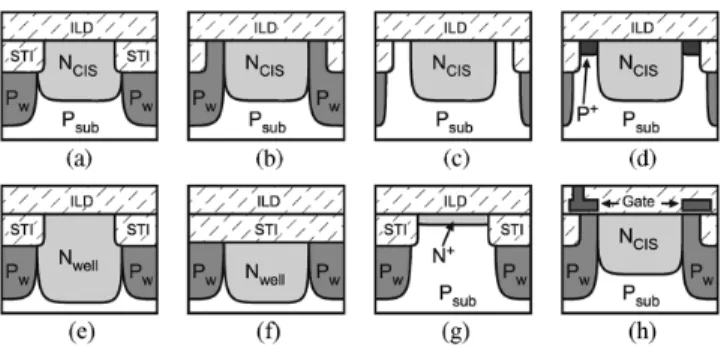
Fig. 1. Simplified cross section of the following thick oxide FETs: (a) FOXFET, (b) ILDFET A with STI around, (c) ILDFET B with no STI. Every structure has a 300mwide and 0.84mlong gate region.
Fig. 2. Field oxide FET subthreshold characteristics, before irradiation, after 1 kGy and after 168 h 100 Cannealing. Irradiation and annealing were performed with two gate bias conditions: biased(V = 3:3 V)and grounded.
A. Thick Oxides
Thick oxides, STI and ILD, were characterized thanks to the 300 wide and 0.84 long field effect devices presented in Fig. 1. Both and photodiode optimized N implants ( implants) are well suited for drain and source implantation of such device. Since we are particularly interested in the imaging related features, we chose to use the implant. The first presented device (Fig. 1(a)) is a classical field oxide field ef- fect transistor (FOXFET), the MOS structure is constituted by a polysilicon gate, STI as insulator and as semiconductor.
The is formed by a large number of process steps, and its doping profile is quite complex and is not known precisely.
In the ILDFETs the polysilicon gate is replaced by a first level metal layer and the STI by an ILD layer. The first one, ILDFET A (Fig. 1(b)), is surrounded by STI in contrast to the transistor B (Fig. 1(c)) on which the field oxide has been completely re- moved.
FOXFET subthreshold characteristics are presented in Fig. 2 before and after -ray exposure. During irradiation, one device was biased with the worst case configuration [7]—gate at 3.3 V and all other terminals grounded—whereas the other was grounded. As usually observed, a trapped charge induced threshold voltage shift and an interface state induced sub- threshold slope decrease are induced by irradiation and the applied electric field enhances the effects. The extracted [8]
interface state density increase and trapped charge density increase are shown in Table I. Inter device leakage can be estimated from this plot: in the worst case scenario, assuming a polysilicon strip deposited between two 300 wide devices,
TABLE I
TRAPPEDCHARGEDENSITIES(1N )ANDINTERFACETRAPDENSITIES (1N )INCREASESINDUCED BYIONIZINGRADIATION IN THETESTED
THICKOXIDEFETs AFTERIRRADIATION ANDAFTER168 h 100 C ANNEALING ATTWOBIASINGCONDITIONS, (V = 3:3 VANDGROUNDED).
TRENCHCORNERDENSITIESWEREEXTRACTEDFROM THEPARASITICFET SUBTHRESHOLDSLOPE(ILDFET A, FIG. 3)
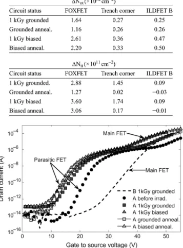
Fig. 3. ILDFET A, (with STI around), subthreshold characteristics, before irra- diation, after 1 kGy and after 168 h 100 Cannealing. Irradiation and annealing were performed with two gate bias conditions: biased(V = 3:3 V)and grounded. One ILDFET B subthreshold characteristics is also plotted for com- parison.
the inter device leakage current after 1 kGy could grow up to 0.1 for a 3.3 V gate voltage. This worst case current would be reduced to a value far smaller than 1 nA with realistic device sizes. The drain junction reverse current also increases significantly with absorbed dose. This will be analyzed in detail in the photodiode section.
After the accelerated annealing step, a relatively small part of the trapped charge (15–30%) is removed. This is thought to be due to the large oxide thickness, the weak electric field, ( 0.1 MV/cm), and the presence of oxide bulk hole traps [9].
The different nature of thermally grown gate oxides and double layer (thermally grown and chemical vapor deposited) trench dielectrics can also be a reason for this weak recovery. Indeed, double layer is known to have a different behavior than single layer thermally grown oxide under irradiation [10]. An- other surprising result, is the apparent annealing of interface traps after the 100 step. Whereas such an effect is not ex- pected in thermally grown MOS oxides [11], similar behavior
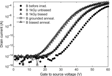
Fig. 4. ILDFET B, (without STI), subthreshold characteristics, before irradi- ation, after 1 kGy and after 168 h 100 Cannealing. Irradiation and annealing were performed with two gate bias conditions: biased,(V = 3:3 V), and grounded.
has been recently observed in deep submicron CMOS STI [12], and was previously seen in thick bipolar oxides [13] or when the applied electric field is relatively small [14]. The real cause of this phenomenon goes beyond the scope of this paper and should be studied in detail in future work.
The measurements performed on ILDFETs are shown in Fig. 4. The transistor A curve exhibits two humps indicating the presence of a parasitic transistor. The fact that ILDFET B does not show such behavior indicates that the hump is due to the surrounding STI. The parasitic transistor is most likely located in the trench corner region [15], [16]. Therefore, a qualitative analysis of the trench corner degradation can be inferred from ILDFET A measurements in contrast to the ILD oxide which has to be studied with ILDFET B structure. Reverse junction leakage increases only appear on the MOST surrounded by STI, therefore STI is also responsible for this radiation induced leakage current. Except for this double hump behavior, irradia- tion effects are similar but less intense than those observed on FOXFETs. It is interesting to notice, in Table I, that ionizing radiation induced much more trapped charges and interface states in the STI oxide than in the ILD oxide. As regards the STI corner region, it behaves almost like the ILD from the trapped charge point of view but is an important source of radiation induced interface states.
Regarding the annealing behavior, ILDFET and parasitic trench corner FET do not exhibit any significant trapped charge annealing. In addition to assumptions previously mentioned for FOXFETs, a dominant deep level hole trap in the ILD could be the cause of this non recovery. On the contrary, almost all the interface states generated in the trench corner parasitic FET seem to disappear after the one week annealing step. ILDFET B interface traps seem to have a similar behavior, but their density corresponds to the measurement accuracy limit and is not reliable.
B. Gate Oxide
The same study was conducted on the gated diodes [17] pre- sented in Fig. 5. This structure has two gates that allows one
Fig. 5. Cross sectional view of the designedN gated diode with gate 2 grounded. (a) atV = 0 V. (b) atV > 1:6 V. The depleted region limit is represented by the dashed line.
Fig. 6. Gated diode reverse current versus gate 1 voltage. The diode is reverse biased to 2 V, theN ring is floating and the second gate is grounded.
to study the gate oxide and the STI oxide independently. The floating ring is used to connect the two depletion regions.
The gate 2 current contribution is dominated by the STI corner/
sidewall generation current, since this gate is very short in com- parison to gate 1. For this qualitative approach, gate bulk gen- eration currents are neglected as compared to the other contri- butions. This particular device has no , hence the P surface doping density is very low, allowing the formation of a deple- tion layer even at low negative gate voltages. Fig. 6 presents the gated diode current increase with irradiation at 2 V junction re- verse bias. Both, gate 1 and diffusion were biased to 3.3 V during irradiation and annealing. As expected on thin gate ox- ides [18], no voltage shift is noticeable indicating that a negli- gible amount of trapped charge is induced by irradiation.
For gate 1 voltages ranging from 2 V to 0.65 V, the silicon region under gate 1 is in the accumulation regime and the mea- sured current corresponds to the junction reverse cur- rent. This reverse current is dominated by a gate voltage depen- dent parasitic surface current in the gate to diffusion overlap region and is often referred to as gate induced drain leakage (GIDL). The electric field in the overlap region is known to rise with increasingly negative gate voltage [19]. This growing elec- tric field leads to enhanced thermal generation current [20] and interface trap assisted tunneling (ITAT) current [21]. These two contributions are enhanced by interface traps and are most likely the cause of the radiation induced gated diode current increase in the accumulation regime [22].
From 0.65 V to 1.5 V (see Fig. 5(a)), the silicon regions under gate 1 and 2 are depleted and the dominant currents are the gate 1 surface generation current and the STI trench sidewall generation current. For higher gate voltages, the gate 1 region
is inverted (see Fig. 5(b)) and the STI interface becomes the major contributor. It is then possible to discriminate STI and gate oxide interface contributions as illustrated in Fig. 6. The STI current increases from 0.1 before exposure to 6.4 after 1 kGy. The gate surface generation current is also increased by a noticeable amount: from 8.2 before irradiation to 31 after 1 kGy. This last result can lead to a qualitative approximation of the radiation induced interface trap density [17]:
(1) where is the elementary charge, the gate 1 area, the thermal velocity and the intrinsic carrier concentration. The effective capture cross section is expected [7] to range from
to and a value close to is usually
reported [17], [23]. Taking this last value for the capture cross section and for the thermal velocity yields a of , which is negligible in comparison to Table I values. After annealing, the STI leakage current is reduced by more than 50% (2.8 ) whereas a noticeable buildup [7], [24] of interface states brings the interface trap density to
. This buildup is confirmed by the gate overlap region current increase in accumulation mode (for gate voltage below
0.65 V) after the annealing.
Gate leakage was also investigated and it stayed below the measurement resolution, even on MOS capaci- tors. Therefore, the gate leakage current density stayed below 1
, even after 1 kGy.
IV. DEVICECHARACTERIZATION
A. Photodiodes
Total dose effects on “in-pixel” photodiodes, MOSFET source and MOSFET drain leakages have been studied thanks to several test diodes. Since our study focuses on the imaging features, all the test structures were designed with the dedicated
“in-pixel” . Several area-over-perimeter ratios were drawn to separate perimeter and area contributions. Most of the test structures are about to ensure a sufficient measured current. On almost all the structures, no significant difference was observed between biased and grounded devices during irradiation and annealing. Thus, only results of devices reverse biased to 3.3 V during irradiation and annealing are presented.
All the structures were surrounded by a ring to prevent parasitic inter device leakage.
Fig. 7 presents a cross sectional view of the test diodes.
As mentioned previously, in addition to the classical and diodes (Fig. 7(g) and 7(e)), this technology offers an N implant dedicated to the design of optimized photodiodes ( implant) for CMOS image sensors. The three recessed field oxide diodes (RFD) presented in Fig. 7(b), 7(c) and 7(d) are CIS photodiodes with recessed field oxides. We chose to use a large recess distance, about 5 to insure that the depletion region can not reach the STI sidewall. The first RFD version has a around it as illustrated in Fig. 7(b) whereas the second is directly surrounded by the P epitaxial layer ( , Fig. 7(c)) and the third (7d) by
Fig. 7. Test photodiode simplified cross sections: (a) standard CIS diode, (b) RFD0P , (c)RFD0P , (d)RFD0P , (e)N diode, (f)N 0STI diode, (g)N diode and (h) gated photodiode.
a heavily doped implant . The
structure (Fig. 7(f)) is an diode entirely covered up by the STI oxide, except on the small contact regions. Finally, the gated photodiode structure is surrounded by a polysilicon gate (Fig. 7(h)).
Reverse current of diodes versus total dose is shown for a 2.4 V reverse bias in Fig. 8. All the structures ex- hibit a current rise with total dose and recover the main part of the degradation after the annealing step. The dark current
plots of , , and
diodes (see Fig. 9 reproduced from [25]) sug- gest that this current is mainly a generation current caused by the junction perimeter. The CIS diode reverse current activation energy was found to be close to 0.63 eV before and after expo- sure to -ray, which confirms the generation current hypothesis.
The generation current is known to increase with the number of generation centers located in the depletion region. Ionizing radi- ation can lead to this parasitic effect by extending the depletion region, because of STI trapped charges, or by generating a large number of interface states into it. STI characterization results presented previously (Fig. 2) suggest that both phenomena are involved in the CIS diode dark current increase. However, the significant annealing behavior tends to indicate that interface states play an important role. One can also notice in Fig. 8 that CIS, and structures show exactly the same response with irradiation, indicating that the N region does not play a significant role in the process. Hence, it can be inferred that the depletion region extension in the region, along the trench bottom is the main generation site. This is confirmed by RFD diodes behaviors. The has a higher dark cur- rent value before irradiation because of a lower doping density at the surface of the than below the STI, and then a larger lateral depletion region extension. However, the dark current in- crease with irradiation is quite small in comparison to CIS diode thanks to the small amount of radiation induced interface states in ILD with respect to STI (Table I). The structure exhibits the largest dark current before and after irradiation be- cause the doping density is low enough to allow the de- pleted region to reach the STI sidewalls, despite the large recess distance. Before and after irradiation, an exponential tunneling current, greater than 1 nA at 0 V, was observed on re- sults and this current is not shown in Fig. 8 for practical reasons.
This huge leakage is due to the very high electric field induced by the implant. The significant junction reverse
Fig. 8. Test photodiode dark current increase with irradiation and annealing at 2.4 V reverse bias. The presented results correspond to2000 2 5 m photo- diodes biased during irradiation and annealing.
Fig. 9. CIS diode dark current at 2.4 V reverse bias versus perimeter. The following photodiode dimensions were used10 2 10 m ,500 2 20 m , 100 2 100 m and2000 2 5 m .
current is supposed to be caused by the high interface state den- sities of the trench sidewalls and the light P doping density, since the has not been extended below the diffusion in this particular test structure.
During measurement, the gate of the gated photodiode was biased at the accumulation threshold voltage shown in Fig. 6. In contrast to the gated diode presented in Section III-B, this accumulation voltage was equal to 0.45 V in this photodiode. Placing the gate at the accumulation limit prevents the extension of the depleted region below the gate and isolates the photodiode from the surrounding STI. Moreover, this accumulation threshold also corresponds to the minimum GIDL effect. Decreasing further the gate voltage leads to an enhanced soft breakdown current, as discussed in Section III-B.
Fig. 8 shows that before irradiation, biasing the gate to the accumulation point works fine and the dark current achieved is close to the optimized CIS photodiode one. Unfortunately, as already observed on the gated diode, ionizing radiation generates enough interface states to dramatically increase this dark current and induce a soft breakdown at very low voltage.
This soft breakdown exponential behavior was clearly observed
on additional cathode current versus cathode voltage measure- ments.
Biasing conditions during annealing appeared to have a sig- nificant impact on the gated photodiode whereas no difference was seen between biased and grounded devices just after irradi- ation. On one hand, the diode reverse biased during annealing recovered pretty well as shown in Fig. 8. On the other hand, the dark current of the grounded device during annealing rose from 1.4 pA to 1.6 pA like the gated diode of Section III-B.
Knowing that for both gated photodiodes the gate was grounded and that in the gated diode, both gate and N diffusion were biased to the same potential, it can be inferred that interface state buildup during annealing only appears when no potential differ- ence exists between the N diffusion and the gate. The fact that the interface trap buildup is inhibited, when the N diffusion is biased to 3.3 V and the gate is grounded, is most likely due to the direction of electric field which repulses the ion, the source of interface states [7], from the sensitive high electric field gate overlap region. If this conclusion is correct, this would mean that biasing the gate to a positive voltage with respect to the N diffusion will lead to an enhanced interface trap buildup in these gated diodes.
B. N Channel MOSFET
Two families of N-MOSFETs are available in this tech- nology: “regular” and “in-pixel” transistors. In-pixel MOSTs are supposed to be used in the pixel area of an image sensor. As mentioned previously, this area has a dedicated doping profile to improve the photodiode collection efficiency. There- fore, additional P implants are used to make the “in-pixel”
devices behave like “regular” ones without impacting the photodiode performances. Moreover, the channel implant can be reduced to tune the threshold voltage , leading to the following three device types: standard threshold voltage (SVT), low threshold voltage (LVT) and zero threshold voltage (0VT) transistors. These structures can be used inside or outside the pixel area, which leads to a total of six different device types.
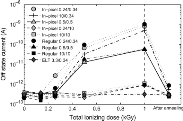
Fig. 10 presents the off-state drain current evolution with total dose for standard MOSTs. This off-state current is mea- sured when the source and gate are both grounded. Prelimi- nary results obtained last year [25] on some “in-pixel” NMOST are presented in this figure for comparison with “regular” ones.
Note that both “regular” and “in-pixel” devices behave exactly the same despite their different constitution. The para- sitic off-state current is clearly increasing with total dose and decreases after the annealing step. The degradation is strongly attenuated when the gate length increases from 0.34 to 0.5 and then to 10 while it is quite insensitive to the channel width. This indicates that this current is a well known edge leakage current [26] due to charge trapping in the STI. This is in good agreement with the FOXFET threshold voltage shift shown in Section III-A. This was also confirmed by similar mea- surements on several types of edgeless FET which did not ex- hibit any degradation with total dose. The enclosed layout tran- sistor (ELT) plot in Fig. 10 illustrates this immunity. The same tests were conducted on 0VT and LVT devices. These devices suffered from higher edge leakage currents, between one and two decades larger, because the parasitic transistor threshold
Fig. 10. N channel FETs leakage current versus total dose measured with V = 0:5 Vand all other terminals grounded. These devices were biased with worst conditions. The W/L aspect ratios are shown in[m]=[m]. Post annealing values are also shown.
voltage is also lowered when the channel P doping density is lowered.
As expected for deep submicron technology [18], no change in threshold voltage or subthreshold slope was observed on any of these devices. This could also have been inferred from gate oxide characterization results which showed no trapped charges effect and negligible interface state buildup.
C. P Channel MOSFET
One minimum size P channel transistor with
and was designed and total dose tested. In contrast to the N-MOSFETs, Fig. 11 shows that the 0.24/0.34 P-MOST undergoes a large threshold voltage (about 0.9 mV/Gy) shift when irradiated. The transistor becomes less conducting with dose. The threshold voltage recovers partially after the annealing step. In order to understand the degradation we studied the P-MOST readout chain transfer function of the pixel array located on the same die. This transfer function uses three P channel transistors with the following W/L ratios : 7.5/0.34, 11/0.75 and 68/3.5. After irradiation, a slight change in the non linear part of the transfer function was observed and the 7.5/0.34 device was identified to be responsible for it. This transistor exhibited a very small shift (about 0.05 mV/Gy). No change that can be attributed to the two largest transistors was observed. Therefore, the 11/0.75 and 68/3.5 MOST were not degraded by irradiation.
This suggests that the effect disappears when the channel width decreases. Therefore, the gate oxide does not seem responsible, as expected by gate oxide characterization results.
All these observations suggest a radiation induced narrow channel effect (RINCE) [27]. It should be pointed out that the RINCE presented in Fig. 11 is much larger than similar effects observed in other technologies. This RINCE agrees with the STI trapped charge effects mentioned in the previous sections. Fur- thermore, as expected for P channel transistors, no leakage cur- rent variation was measured.
Fig. 11. Minimum size P channel MOS transistor threshold voltage shift as a function of absorbed ionizing dose and after annealing.
Fig. 12. Simple 3T active pixel readout path schematic. The functional stages are separated by gray dashed lines.
V. DISCUSSION
A. Expected Effect on Sensors
The aim of the previous sections was to identify, locate and understand the ionizing radiation effects, up to 1 kGy, on every piece of a CMOS image sensor readout chain for future radiation hardening. A simple classical readout path of a three transistor active pixel sensor (3T APS) is shown in Fig. 12. Presented re- sults on P-MOST imply that if minimum size P channel transis- tors are not used in the design, the P-MOST readout chain will not be degraded by irradiation. The rest of the circuit is consti- tuted by N-MOSFETs and a photodiode. The only degradation observed on the N-MOST irradiated with worst-case biasing was an off-state current increase reaching a maximum value of 1 nA. Inter device leakage was also estimated to be smaller than 1 nA. Such leakage would not be sufficient to impact the sampling stage in normal operating conditions, especially if we take into account substrate effect and the fact that the gate to source voltage of the sampling transistor is negative when the transistor is off. Regarding the current source used to bias the N-MOST readout chain, the provided bias current is several or- ders of magnitude greater than the leakage current. Hence the N-MOST chain source follower and switch transistors leakage currents are also negligible.
However, leakage currents become critical before the charge to voltage conversion. The physical frontier between the charge collection node and the voltage signal path is the source follower gate oxide. It has been shown that gate leakage current is smaller than 1 , which can be completely neglected in front of photodiode intrinsic dark current presented in this article. Inter device leakage could play a role in the photodiode dark current degradation. However Fig. 2 shows that for an unbiased field
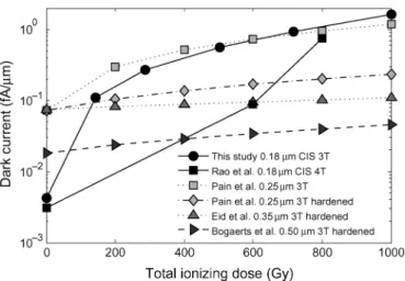
Fig. 13. Comparison of ionizing radiation induced dark current increase on image sensors manufactured with several CMOS technologies. Dark current has been divided by photodiode perimeter for comparison purpose. Some of the presented data comes from hardened by design CMOS APS. All the results were measured at, or extrapolated to 23 C.
oxide, which is usually the case around the photodiode, the drain to source leakage is negligible. This is even more true if we consider a realistic device size.
When it is turned off, the reset transistor can still change the collection node voltage through its drain to source leakage cur- rent. It is assumed that under normal operating conditions during irradiation the reset MOSFET has a negligible leakage current.
This has been verified on an additional test chip. The following operating conditions were applied to the tested transistor during irradiation: drain to 3.3 V, source to 2.4 V, which corresponds to a realistic photodiode cathode voltage, and gate pulsed between 0 and 3.3 V with the same duty cycle than in an operated APS.
The leakage current of this minimum size transistor at zero gate and source voltages stayed below 1 pA after 1 kGy, instead of the 1 nA measured with worst case biasing. Taking into account the fact that the reset MOST is biased with negative gate to source voltage when turned off, this leakage current drops below 1 fA and is then limited by source junction leakage.
We can infer from this qualitative analysis that up to 1 kGy the only ionizing radiation effect that should be seen on an unhard- ened CMOS image sensor manufactured using this technology is a dark current increase coming from a depletion region exten- sion around the photodiode junction and the reset MOST source reverse current. This assumption has been verified on the CMOS sensor located on the same die as the test struc- tures [25]. This imager exhibited only an elevated dark current increase (Fig. 13) which corresponded well with estimation from CIS diode results presented here, taking into account perimeter ratio between test diode and pixel diode. Furthermore, pixel ar- rays with enclosed layout transistors and guard rings were also total dose tested and no change in dark current degradation was observed, except a little reduction due to the elimination of reset MOSFET source leakage. This confirms that MOSFET leakage and inter device leakages are negligible, at least up to 1 kGy.
B. Comparison With Previous work
In order to evaluate the total dose sensitivity of the chosen technology, it can be interesting to compare our results to pre-
vious data [3], [5], [6], [28]. These studies were performed on different technologies with or without hardened design tech- niques. Since we have shown that the dark current increase is only caused by the perimeter, it seems more appropriate here to compare the dark current per unit of perimeter length rather than per unit of area. This linear density was retrieved by multiplying the given dark current values in by the pixel area and then by dividing the result by the photodiode perimeter. This perimeter was explicitly mentioned in the selected papers or the pixel layout was available and the perimeter was directly mea- sured. Regarding the irradiation steps, all the data except Raoet al.data [28] were linearly interpolated from 0 to 1 kGy. Finally, the linear dark current density was extrapolated to 23 thanks to a classical [1] 0.63 eV activation energy if no activation en- ergy was provided. The data we used for the comparison comes from the 128 128 3T APS array manufactured on the same die as the test structures described in this paper.
The comparison is illustrated in Fig. 13. First, it can be seen that this optimized CMOS sensor technology has a fairly low dark current linear density. Indeed, only the pinned photodiode dark current is smaller before irradiation. This is expected since the pinning implant and the used in 4T technologies are designed to restrict the contact between the depletion region and the surrounding oxides. After irradiation, the 0.18 3T APS dark current is rising quickly to become the worst at 1 kGy.
This indicates that sensors manufactured with this process are much more sensitive to ionizing radiation than the other arrays presented here. Even the older unhardened technologies exhibit better radiation hardness.
C. Consequences for Sensor Design
Up to 1 kGy, the sensor radiation hardness can be improved by using an enclosed layout design to reduce the reset MOSFET source reverse leakage current, and by finding an efficient way to reduce the photodiode dark current increase. The use of pinned photodiodes can be a good way to reduce this dark current but 4T technologies are not yet enough mature to be used in space applications. It has been shown that is a fairly good solution but it leads to an elevated dark current before irradi- ation. Since the identified weak point is the number of traps in the depletion region extension at the surrounding interface, improved hardness can be provided by the use of ILD or gate oxide instead of STI as surrounding oxide. However the surface P doping density has to be optimized to reduce the surface de- pletion width. A low dark current can be achieved with a implant but the distance between and implants has to be optimized to reduce the maximum electric field, and to avoid tunneling effects, without allowing a too large depleted region extension. The gated photodiode solution is still considered but as for the implant an optimal distance has to be found to avoid the gate overlap effect without enlarging the depleted re- gion too much.
For higher total ionizing doses, in addition to hardened by design photodiodes, edgeless transistors still have to be used for NMOSTs to prevent critical leakage currents. rings must also be used to avoid inter device leakage which can become im- portant, and minimum size P channel FETs have to be avoided or protected from RINCE by enclosed layout techniques.
VI. SUMMARY ANDCONCLUSION
The ionizing radiation tolerance of a 0.18 CMOS image sensor technology for the design of CMOS sensors was eval- uated. Pixel array and elementary devices such as FOXFET, ILDFET, gated diodes, photodiodes and MOSFETs were total dose tested up to 1 kGy. Total dose caused generation current increases in photodiodes and pixel arrays, edge leakage cur- rents in small N-MOSFETs, large RINCE shifts in min- imum size P-channel transistors and significant augmentation of gated diode generation currents. This last current was attributed to gate interface states and all the other degradations were at- tributed to the shallow trench isolation as a result of the oxide characterizations. The study of the thick oxides STI and ILD, appeared necessary to understand the observed degradation, es- pecially after the annealing step. Unusual behaviors after the annealing of the thick oxides suggest that the 168 h 100 re- sults can be misinterpreted without complementary oxide char- acterizations. This work emphasizes the need to use efficient techniques to reduce the influence of STI on photodiode reverse current in order to design radiation hard CMOS sensor in deep submicron technologies. The use of hardened N-MOSFETs has to be discussed regarding the imager design requirements and minimum size PMOST should be avoided or hardened, with en- closed layout techniques for example. Future work will focus on designing an ionizing radiation hard CMOS sensor in this tech- nology.
ACKNOWLEDGMENT
irradiation opportunities given by T. Nuns, J.-P. David, S. Duzellier, S. Guivarch and G. Hubert from ONERA are grate- fully acknowledged. The authors thank P. Malisse and Euro- practice-IMEC team for their great support. The authors also thank C. Duprat from INSA-AIME, C. Engel, P. Cervantes, P.
Pinel, F. Corbière, N. Huger and L. Boucher from ISAE for their help with circuit design, packaging and experimental is- sues. S. Guiry, F. Larnaudie and N. Guardiola (Astrium) are also thanked for their assistance.
REFERENCES
[1] G. R. Hopkinson, “Radiation effects in a CMOS active pixel sensor,”
IEEE Trans. Nucl. Sci., vol. 47, no. 6, pp. 2480–2484, Dec. 2000.
[2] M. Cohen and J.-P. David, “Radiation-induced dark current in CMOS active pixel sensors,” IEEE Trans. Nucl. Sci., vol. 47, no. 6, pp.
2485–2491, Dec. 2000.
[3] E.-S. Eid, T. Y. Chan, E. R. Fossum, R. H. Tsai, R. Spagnuolo, J. Deily, W. B. Byers, and J. C. Peden, “Design and characterization of ionizing radiation-tolerant CMOS APS image sensors up to 30 Mrd (Si) total dose,”IEEE Trans. Nucl. Sci., vol. 48, no. 6, pp. 1796–1806, Dec. 2001.
[4] B. R. Hancock, T. J. Cunningham, K. P. McCarty, G. Yang, C. J.
Wrigley, P. G. Ringold, R. C. Stirbl, and B. Pain, “Multi-megarad (Si) radiation-tolerant integrated CMOS imager,” inProc. SPIE, 2001, vol.
4306, pp. 147–155.
[5] J. Bogaerts, B. Dierickx, G. Meynants, and D. Uwaerts, “Total dose and displacement damage effects in a radiation-hardened CMOS APS,”
IEEE Trans. Electron Devices, vol. 50, no. 1, pp. 84–90, 2003.
[6] B. Pain, B. R. Hancock, T. J. Cunningham, S. Seshadri, C. Sun, P.
Pedadda, C. J. Wrigley, and R. C. Stirbl, “Hardening CMOS imagers:
Radhard-by-design or radhard-by-foundry,” inProc. of SPIE, 2004, vol. 5167, pp. 101–110.
[7] T. P. Ma and P. V. Dressendorfer, Ionizing Radiation Effects in MOS Devices and Circuits. New York: Wiley-Interscience, 1989.
[8] P. J. McWhorter and P. S. Winokur, “Simple technique for separating the effects of interface traps and trapped-oxide charge in metal-oxide- semiconductor transistors,”Appl. Phys. Lett., vol. 48, pp. 133–135, Jan.
1986.
[9] H. E. Boesch, Jr. and F. B. McLean, “Hole transport and trapping in field oxides,”IEEE Trans. Nucl. Sci., vol. NS-32, no. 6, pp. 3940–3945, Dec. 1985.
[10] K. Watanabe, M. Kato, T. Okabe, and M. Nagata, “Radiation hardened silicon devices using a novel thick oxide,”IEEE Trans. Nucl. Sci., vol.
NS-32, no. 6, pp. 3971–3975, 1985.
[11] A. Lelis, T. Oldham, and W. DeLancey, “Response of interface traps during high-temperature anneals,”IEEE Trans. Nucl. Sci., vol. 38, no.
6, pp. 1590–1597, 1991.
[12] F. Faccio, H. J. Barnaby, X. J. Chen, D. M. Fleetwood, L. Gonella, M.
McLain, and R. D. Schrimpf, “Total ionizing dose effects in shallow trench isolation oxides,”Microelectron. Rel., to be published.
[13] M. Shaneyfelt, J. Schwank, D. Fleetwood, R. Pease, J. Felix, P. Dodd, and M. Maher, “Annealing behavior of linear bipolar devices with en- hanced low-dose-rate sensitivity,”IEEE Trans. Nucl. Sci., vol. 51, no.
6, pp. 3172–3177, Dec. 2004.
[14] D. Fleetwood, P. Dressendorfer, and D. Turpin, “A reevaluation of worst-case postirradiation response for hardened MOS transistors,”
IEEE Trans. Nucl. Sci., vol. NS-34, no. 6, pp. 1178–1183, Dec. 1987.
[15] T. Iizuka, K. Chiu, and J. Moll, “Double threshold MOSFETs in bird’s- beak free structures,” inProc. IEDM Tech. Dig., 1981, vol. 27, pp.
380–383.
[16] M. Shaneyfelt, P. Dodd, B. Draper, and R. Flores, “Challenges in hard- ening technologies using shallow-trench isolation,”IEEE Trans. Nucl.
Sci., vol. 45, no. 6, pp. 2584–2592, Dec. 1998.
[17] A. S. Grove and D. J. Fitzgerald, “Surface effects on p-n junctions:
Characteristics of surface space-charge regions under non-equilibrium conditions,”Solid-State Electron., vol. 9, no. 8, pp. 783–806, 1966.
[18] H. J. Barnaby, “Total-ionizing-dose effects in modern CMOS technolo- gies,”IEEE Trans. Nucl. Sci., vol. 53, no. 6, pp. 3103–3121, Dec. 2006.
[19] A. Grove, O. Leistiko, Jr., and W. Hooper, “Effect of surface fields on the breakdown voltage of planar silicon pn junctions,”IEEE Trans.
Electron Devices, vol. ED-14, no. 3, pp. 157–162, Mar. 1967.
[20] M. J. J. Theunissen, “Analysis of the soft reverse characteristics of n+p drain diodes,”Solid-State Electron., vol. 28, pp. 417–425, 1985.
[21] I. Chen, C. Teng, D. Coleman, A. Nishimura, T. Inc, and T. Dallas,
“Interface trap-enhanced gate-induced leakage current in MOSFET,”
IEEE Electron Device Lett., vol. 10, no. 5, pp. 216–218, May 1989.
[22] T. Chang, C. Huang, and T. Wang, “Mechanisms of interface trap-in- duced drain leakage current inoff-state n-MOSFET’s,”IEEE Electron Device Lett., vol. 42, no. 4, pp. 738–743, Apr. 1995.
[23] E. Nicollian and A. Goetzberger, “TheSi 0 SiO interface-electrical properties as determined by the metal-insulator-silicon conductance technique,”Bell Syst. Tech. J, vol. 46, pp. 1055–1133, 1967.
[24] J. Schwank, D. Fleetwood, M. Shaneyfelt, P. Winokur, C. Axness, and L. Riewe, “Latent interface-trap buildup and its implications for hard- ness assurance,”IEEE Trans. Nucl. Sci., vol. 39, no. 6, pp. 1953–1963, Dec. 1992.
[25] V. Goiffon, P. Magnan, F. Bernard, G. Rolland, O. Saint-Pe, N. Huger, and F. Corbiere, “Ionizing radiation effects on CMOS imagers manu- factured in deep submicron process,” inProc. SPIE, 2008, vol. 6816, no. 7, pp. 1–12.
[26] R. Lacoe, “CMOS scaling, design principles and hardening-by-design methodologies,” inIEEE NSREC Short Course, 2003.
[27] F. Faccio and G. Cervelli, “Radiation-induced edge effects in deep sub- micron CMOS transistors,”IEEE Trans. Nucl. Sci., vol. 52, no. 6, pp.
2413–2420, 2005.
[28] P. R. Rao, X. Wang, and J. P. Theuwissen, “Degradation of CMOS image sensors in deep-submicron technology due to-irradiation,”
Solid-State Electron., vol. 52, no. 9, pp. 1407–1413, 2008.