A 73.1dB SNDR Digitally Assisted Subsampler
for RF Power Amplifier Linearization Systems
The MIT Faculty has made this article openly available.
Please share
how this access benefits you. Your story matters.
Citation
Chung, SungWon and Joel L. Dawson. "A 73.1dB SNDR Digitally
Assisted Subsampler for RF Power Amplifier Linearization
Systems." 6th International Symposium on VLSI Technology,
Systems and Applications (2009 VLSI-TSA), 27-29, April 2009,
Hsinchu, Taiwan. © 2009 VLSI-TSA.
As Published
http://vlsitsa.itri.org.tw/2009/General/
Publisher
VLSI-TSA
Version
Final published version
Citable link
http://hdl.handle.net/1721.1/60412
Terms of Use
Article is made available in accordance with the publisher's
policy and may be subject to US copyright law. Please refer to the
publisher's site for terms of use.
148
978-4-86348-010-0 2009 Symposium on VLSI Circuits Digest of Technical Papers14-4
A 73.1dB SNDR Digitally Assisted Subsampler for RF Power Amplifier Linearization Systems
SungWon Chung and Joel L. Dawson
Microsystems Technology Laboratories, Massachusetts Institute of Technology, Cambridge, MA 02139, USA E-mail: [email protected]
Abstract
We present a digitally assisted subsampler, designed to serve as the downconversion path in adaptive predistorters for 800MHz–5.8GHz RF power amplifiers. We use digital averaging to overcome the noise folding problems of subsampling, obtaining a final SNDR of 73.1dB for signals centered about a 2.4GHz carrier. Using quadra-ture subsampling, we obtain both the I and Q samples from the same physical path and thereby eliminate IQ gain mismatch. When used as part of an adaptive predistortion system, the subsampler enables an EVM improvement of 3.2% and distortion products suppression of up to 7.6dB for 802.11g signals. The subsampler IC, designed in a 90nm CMOS process, consumes 6.0mW from a 1.2V supply.
Introduction
Subsampling is recognized as an energy-efficient signal pro-cessing technique for highly digital transceivers [1]–[3]. However, subsamplers are notorious for low SNR performance due to noise folding, and for stringent requirements for anti-aliasing prefilters. This combination of faults has largely undermined their use in high performance receivers. In transmitters, however, the situation is
fundamentally different. The signal environment has fewer extreme
aggressors, such as blockers, and the transmitted data is often known in advance of actual transmission. This last fact enables the use of averaging and other signal processing techniques to overcome the noise folding problem.
In this paper we describe a subsampler IC for an adaptive predis-tortion system. Fig. 1 shows the architecture of the overall system. A set of training symbols are transmitted, and the PA output is sampled using the subsampler. The digitally processed subsampler output is used to populate the look-up table (LUT). Placing this LUT in the feedback path of ∆Σ modulators accomplishes the inversion of the PA nonlinearity, as well as the interpolation between LUT entries [4]. In the remaining paragraphs, we describe the details of the subsampler IC, the digital signal processing used to obtain a high SNDR, and present measured results.
Digitally Assisted Subsampler Architecture
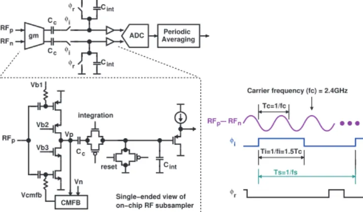
Fig. 2 illustrates the architecture and the operation of the subsampler. For linearity, we limit the subsampler input to less than 150mVpp. As a result, SNDR at the subsampled output is limited to 18-24dB (3-4bits) by the large subsampling noise. To significantly reduce the subsampling noise, we apply digital averaging to the ADC output. To reduce IQ mismatch in gain and phase, quadrature subsampling is implemented with a single path. The principle behind quadrature sampling is that I and Q samples can be obtained serially from the same RF signal path if their corresponding sampling instants are offset by a Tc/4, where
Tc is the period of the RF carrier. For the necessary clock phase
generation, a frequency reference at twice the carrier frequency is necessary.
The subsampling operation is performed by charge integration with a transconductance amplifier (TA) whose current output is accumulated onto an integration capacitor Cint. For better linearity,
a pseudo-differential topology is chosen for the TA. Cascode transistors are used to minimize corruption in the charge integration by providing higher output impedance. The AC coupling capacitor Cc helps to suppress the low-frequency artifacts of even-order
distortion from both the PA and the TA.
A subsampling downconversion path has one difficulty that a
f LO f DAC DAC f 1−z−1 z−1 1−z−1 z−1 Cartesian LUT Delta−Sigma DPD PA f LPF LPF Q’(t) I’ (t) Subsampling f Adaptive Digital Predistortion (DPD) I (t) Q(t) Quadrature ADC
Fig. 1. Adaptive predistortion transmitter architecture with low-power training using RF subsampling. For the prototype, the A/D converter was an EVAL-AD7766-2 test board, all digital signal processing was done in MATLAB, and the D/A conversion was performed by an AFG3102 arbitrary waveform generator. Cc RFp reset Cint Single−ended view of on−chip RF subsampler φr p RFn RF i φ Ts=1/fs Tc=1/fc Ti=1/fi=1.5Tc Carrier frequency (fc) = 2.4GHz Cint φr Cint Cc Cc φr φi φi RFp n RF gm ADC Periodic Averaging integration CMFB Vp Vn Vb1 Vcmfb Vb2 Vb3
Fig. 2. Digitally assisted subsampler architecture. Quadrature sampling is employed (i.e., Q samples are offset from I samples by Tc/4), allowing both the I and Q samples to be obtained from the same physical signal path.
mixer-based approach does not. Even-order nonlinearity in the PA can result in low-frequency products that corrupt the feedback data stream. Baseband digital predistortion cannot compensate for even-order nonlinearity in the PA, so in any predistortion training system it is desirable to reject or ignore these artifacts. A mixer naturally does this by modulating any low-frequency output of the PA back up to the carrier frequency, where it is easily filtered out. In the case of our system, we first modulate the training signals with a 4kHz sinusoid. Then, after subsampling, we process the samples with the averaging operation shown in Fig. 3(a). Samples are collected over a half-period of the 4kHz sinusoid, and samples from many successive half-period windows are averaged to construct a single half-period. This averaging operation requires that, before summation, alternate half-period windows are first inverted. The result is that the random noise is reduced, and even-order distortion products are cancelled out. The distorted I or Q value is then simply the peak value of the resultant half-period.
For our system, four samples are taken for each half-period. With that number of samples, the averaging operation can be viewed as the discrete-time FIR filter shown in Fig. 3(b). The magnitude response of this filter with seven delay elements (representing 8x averaging) is shown in Fig. 3(c).
Measured Results
Fig. 4 shows the measured noise floor of the subsampler proto-type chip, which is sampling at 50MSPS for 4kHz sinusoid training signals modulating a 2.4GHz carrier. Low-frequency spurious tones and a high noise floor limit the SNDR of the subsampler to under 22.9dB, providing an ENOB of 3.5, which is insufficient for most applications, including WLAN systems. With the 16384x averaging
149
2009 Symposium on VLSI Circuits Digest of Technical Papers+ +
Cancelled
+ +
Fundamental tone or odd−order distortion product Even−oder distortion product
noise reduced DC balance restored, time time time time (a) + + z−4 z−4 z−4 (b) 0 0.25 0.5 0.75 1 −20 −10 0 10 20 Magnitude (dB)
Normalized Frequency (xπ radian)
4kHz 12kHz
ADC sampling rate = 32kSPS
(c)
Fig. 3. Digital filtering for subsampling noise reduction: (a) DC filtering and even-order harmonic cancellation (b) FIR filter equivalent representa-tion, and (c) digital-domain frequency response.
0 2 4 6 8 10 12 14 16 −120 −100 −80 −60 −40 −20 0 Frequency (kHz) Amplitude (dBFS) SFDR = 39.9 dB SNDR = 22.9 dB ENOB = 3.5 bit 0 2 4 6 8 10 12 14 16 −120 −100 −80 −60 −40 −20 0 Frequency (kHz) Amplitude (dBFS) SFDR = 75.5 dB SNDR = 73.1 dB ENOB = 11.8 bit
Fig. 4. Measured subsampling noise floor enhancement with a 4kHz sinusoid modulating 2.4GHz carrier: The ENOB is increased from 3.5 to 11.8 after using 16384x averaging.
TABLE I PERFORMANCESUMMARY
Supply voltage 1.2 V
Power dissipation (excluding buffer) 6.0 mW Sampler input frequency 800MHz – 5.8GHz Gain (for 2.4GHz carrier) -14.2 dB SNDR (w/ 16384x avg., for 2.4GHz carrier) 73.1 dB SFDR (w/ 16384x avg., for 2.4GHz carrier) 75.5 dB ENOB (w/ 16384x avg., for 2.4GHz carrier) 11.8 bit
Max. subsampling rate 75 MSPS
Max. input 150 mVpp
Process technology 90nm digital CMOS
applied, the SNDR increases to 73.1dB, providing an ENOB of 11.8.1 Fig. 5 shows that the subsampler provides an ENOB of
higher than 10 with digital averaging for carrier frequencies between 800MHz and 5.8GHz.
Fig. 6 shows the transmitted spectrum with a SiGe SE2528L PA for a WLAN 802.11g/OFDM signal, which has a 6dB peak-to-average power ratio (PAPR). With digital predistortion trained using the subsampler chip, the transmit spectral mask margin is additionally increased by as much as 7.6dB. The measured EVM improves from 7.67% to 4.44%.
Fig. 7 shows the microphotograph of the prototype subsampler chip, which includes on-chip subsampling clock generation cir-cuitry. The active area is 0.12mm2 and the chip dissipates 6.0mW
when subsampling at 50MSPS for 2.4GHz carriers. An on-chip source follower consumes 20mW, and it is used to drive the off-chip, 24bit, 32KSPS, 8.5mW ADC. Table I summarizes the performance of the subsampler chip.
1Theory predicts an ENOB improvement of 7 due to 16384x averaging. Our filter’s cancellation of even-order distortion products accounts for the additional ENOB boost of 1.3.
0.8 1.6 2.4 3.2 4 4.8 5.6 10 10.5 11 11.5 12 12.5 13 13.5 14 ENOB (bits) Carrier Frequency (GHz)
Fig. 5. Measured subsampler ENOB using 16384x averaging with a 4kHz sinusoid modulating carrier frequency between 800MHz and 5.8GHz.
2360 2370 2380 2390 2400 2410 2420 2430 2440 −50 −40 −30 −20 −10 0 Frequency (MHz) Spectrum (dBr) 23.3−dBm WLAN 802.11g/OFDM w/o DPD w/ DPD Transmitter spectral mask
Fig. 6. Measured spectrum of WLAN 802.11g adaptive digital predistortion transmitter whose LUT is trained by the subsampler.
Fig. 7. Prototype chip with the active area of 0.12mm2. The die measures 1mm x 2mm.
Conclusion
A digitally assisted subsampler chip for training adaptive predis-tortion transmitters is implemented. To reduce the noise folding and attenuate low-frequency spurious tones at the subsampler output, digital averaging is proposed. The digital averaging is equivalent to a multiband FIR filter whose passbands center on the training signals and the resultant odd-order distortion products. Additionally, quadrature sampling is employed to eliminate IQ gain mismatch errors in the feedback path. The subsampler chip provides 73.1dB SNDR for 4kHz training signals with 16384x averaging, which corresponds to an ENOB of 11.8 and is sufficient to train adap-tive predistortion transmitters for most standards such as 3G and WLAN.
Acknowledgment
This work was funded in part by the FCRP Focus Center for Circuit & System Solutions (C2S2).
References
[1] H. Pekau et al., “A 2.4GHz CMOS sub-sampling mixer with integrated filtering,” IEEE J. of Solid-State Circuits, pp. 2159-2166, Nov. 2005. [2] S. Karvonen et al., “A quadrature charge-domain sampler with
embed-ded FIR and IIR filtering functions,” IEEE J. of Solid-State Circuits, pp. 507-515,, Feb. 2006.
[3] R. Bagheri et al., “An 800-MHz–6-GHz software-defined wireless receiver in 90-nm CMOS,” IEEE J. of Solid-State Circuits, pp. 2860-2876, Dec. 2006.
[4] H. H. Boo, S. Chung, and J. L. Dawson, “Predistortion using a ∆Σ modulator for automatic inversion of power amplifier nonlinearity,” submitted for publication in Proc. of 2009 IEEE MTT-S Int’l Microwave