Application of Three-Dimensional Circuit Integration to
Global Clock Distribution
by
Erica M. Salinas
Submitted to the Department of Electrical Engineering and Computer Science in Partial Fulfillment of the Requirements for the Degrees of
Bachelor of Science in Electrical Engineering and Computer Science and Master of Engineering in Electrical Engineering and Computer Science
at the Massachusetts Institute of Technology January 2004
Copyright 2003 Erica M. Salinas. All rights reserved. The author hereby grants to M.I.T. permission to reproduce and
distribute publicly paper and electronic copies of this thesis and to grant others the right to do so.
Author_________________________________________________________________ Department of Electrical Engineering and Computer Science
January 2004
Certified by___________________________________________________________ Jim Burns Lincoln Laboratory Thesis Supervisor
Certified by___________________________________________________________ Rafael Reif M.I.T. Thesis Supervisor
Accepted by____________________________________________________________ Arthur C. Smith Chairman, Department Committee on Graduate Theses
Application of Three-Dimensional Circuit Integration to
Global Clock Distribution
by
Erica M. Salinas Submitted to the
Department of Electrical Engineering and Computer Science January 2004
In Partial Fulfillment of the Requirements for the Degree of Bachelor of Science in Electrical Engineering and Computer Science and Master of Engineering in Electrical Engineering and Computer Science
ABSTRACT
As the semi-conductor industry moves towards deep sub-micron designs, efficiency of chip-wide communication is becoming the limiting factor on system performance. One globally distributed signal with significant effect on system performance is the clock signal. In this paper utilization of three-dimensional circuit integration to reduce the negative effects of technology scaling on clock signal distribution is investigated. A design is proposed that removes the clock distribution network from the same active plane as the logical functions of the system and places them on a separate, but electrically connected active plane. Proposed benefits of a three-dimensional distribution network are the reduction of global skew, greater signal
integrity, and an increase in system density. All aspects of the design process are detailed including methodology, simulation tools and verification, interconnect and repeater design, the three-dimensional integration process, and the overall predicted system benefits.
Thesis Supervisor: Rafael Reif
Acknowledgements
Completion of this project was not a singular effort on my part, but was the result of the guidance and support of numerous people around me.
First, I would like to thank the people at Lincoln Laboratory. Jim Burns, my supervisor and office mate, took numerous hours out of his day to answer questions, help me overcome roadblocks, and brighten my day with amusing antics. He also provided professional guidance and encouraged me to achieve at my highest level. Jeremy Muldavin, a colleague, also spent much time with me during the day and over lunch to teach me the basics of RF design. Although his answers to my questions were never as simple as I would have liked, they forced me to put forth that extra effort to come to a true understanding of my project. Additional people at Lincoln Laboratory that were always there to answer any questions, whether they be, project related, homework related, or personal included Carl Bozler, Peter Wyatt, Bruce Wheeler, Chang-Lee Chen, Bob Berger, and Sue Moriarty.
Second, two people at MIT also contributed to my success. Rafael Reif, my undergraduate and thesis advisor, has been with me from the beginning to guide me and help me in times of academic crisis. Also, Anne Hunter, queen of course six, was the person who first introduced me to Lincoln Laboratory. It was the many hours spent in her office that helped me graduate with my bachelors degree and made getting my masters degree possible.
Finally, I would like to thank my friends and family. My mother always told me I could do anything I put my mind to. Through her words of encouragement, her financial sacrifices, and her incredible genes, she gave me the wings to soar to my highest
potential. In loving competition with my sister, I was forced to set my sights high. Her success proved to my family and me that anything was possible. Lastly, I had friends that were there to hold my hand through the rough times and celebrate the good times. Much gratitude goes to Matt Willsey, Josh Yardley, Aaron VanDevender, Michael Artz, and Oscar Murillo.
TABLE OF CONTENTS
Acknowledgements...3 LIST OF FIGURES ...5 LIST OF TABLES...5 CHAPTER 1 - INTRODUCTION...6 CHAPTER 2 - BACKGROUND...7 2.1 Clock Systems... 72.2 Three-Dimensional Circuit Integration... 9
CHAPTER 3 – SYSTEM DESIGN...10
3.1 System Overview... 10
3.2 Methodology... 12
3.3 Simulation Tools ... 12
3.4 Repeater Design... 14
Transistor Modeling and Gate Sizing ...14
Repeater Sizing and Placement...16
3.5 Interconnect Structures ... 17
3.6 RF Simulations and Verification ... 20
Frequency Domain Simulation and Verification ...20
Time Domain Simulation and Verification...22
Models...24
3.7 Three-Dimensional Vias and Stack ... 25
CHAPTER 4 – THREE-DIMENSIONAL FABRICATION ...27
CHAPTER 5 – RESULTS AND APPLICATIONS...30
5.1 Characteristics of the Completed System ... 30
5.2 Benefits ... 32
CHAPTER 6 - CONCLUSION ...34
REFERENCES ...35
Appendix A: Clock Tier Layout ...36
LIST OF FIGURES
Figure 1: Signal with and without attenuation... 8
Figure 2: Clock Skew... 9
Figure 3: (a) Clock Tier 6-Level H-tree (b) Logic Tier 4-Level H-tree ... 11
Figure 4: Schematic of nmos transistor ... 15
Figure 5: Multi-fingered nmos transistor with four gate fingers ... 15
Figure 6: Repeater schematic... 17
Figure 7: (a) Microstrip (b) Coplanar Waveguide ... 18
Figure 8: RC curve for 40 um long line... 20
Figure 9: CPW test structure fabricated in an RF metal stack of... 21
Figure 10: Reproduction of CPW test structure... 21
Figure 11: Comparison of measured and simulated S-parameter data ... 22
Figure 12: Time Domain Simulated and Measured Waveforms ... 23
Figure 13: RLC interconnect model ... 25
Figure 14: 3D stack corresponding... 26
Figure 15: Cross-section of 3D via ... 27
Figure 16: SEM cross-section of two 3D vias ... 27
Figure 17: 3D Fabrication Process Flow ... 29
Figure 18: Final Waveform... 31
LIST OF TABLES
Table 1: Relative widths of transistors... 16Table 2: Layers in 3D stack and corresponding thicknesses ... 26
Table 3: Transistor widths (um); L = 0.2 um... 30
Table 4: Interconnect width and Spacing (um)... 30
Table 5: Final Network Characteristics ... 31
CHAPTER 1 - INTRODUCTION
With each generation leading the semi-conductor industry farther into deep sub-micron designs, whole systems on a single chip are becoming a reality. Consequently, system performance will soon be limited, not by computational power, but by the efficiency of chip-wide communication [1]. The clock signal is one of many globally distributed signals. Its function as a reference to data signals within the system places stringent requirements on the signal’s timing and integrity. One negative effect of technology scaling is the increase in signal delay caused by interconnect lengths remaining relatively constant, while their widths are being decreased along with other feature sizes. With system performance dependent upon global signals such as the clock, any increase in its delay can negatively affect system performance.
One area of research that has promised some relief of the difficulties of global signal distribution is three-dimensional (3D) circuit integration. Conventional integrated circuits are comprised of a single layer of active devices interconnected with multiple wiring levels. MIT Lincoln Laboratory (MITLL) has developed a 3D circuit technology that stacks and electrically connects multiple 2D circuit wafers fabricated in the
laboratory’s fully depleted silicon-on-insulator (FDSOI) fabrication technology.
The system proposed is a three-dimensional clock distribution network. It consists of two tiers; where tier refers to an individual device wafer within a stack. The design places a majority of the clock distribution network on one tier and the logical functions of the system on the other tier. By starting with a known load for each node of the tree, the system was designed backwards to stringently maintain system requirements. Through the utilization of 3D circuit integration, circuit simulation and analysis indicate the
system provides the following benefits: skew is decreased by using a balanced
distribution network; signal integrity is maintained by having minimal spatial limitations placed on the repeaters; and system density is increased because removing the clock distribution network leaves more room for additional logical functions in the same area. Each of these functions in turn can benefit overall system performance, including speed.
A more extensive background on clock systems and 3D circuit integration is given in Chapter 2. Chapter 3 separately addresses aspects of the design including the overall system design, the methodology used, RF simulations and verification, repeater design, the interconnect structures, and finally the 3D stack and vias. Chapter 4 details the 3D circuit integration process. Simulations and results are contained in Chapter 5. Finally, Chapter 6 contains the conclusion.
CHAPTER 2 - BACKGROUND
2.1 Clock Systems
The clock signal is integral to the proper functioning of high-speed VLSI circuits. A globally distributed signal, the clock frequently drives the largest load and operates at the highest speeds within a system. Its function as a reference to data signals within the system requires the signal to be sharp, and have little variability [2]. When properly designed, the clock ensures high system performance and reliability by synchronizing the flow of data within the system while avoiding race conditions and the reduction of system speed due to skew. Technology scaling has greatly affected the clock signal. It has been predicted that in the near future the fraction of total chip area that can be reached in a
single clock cycle will be as low as 2% [1]. Effects such as this and a demanding market have made clock distribution a limiting factor on system performance.
Two problems, attenuation and skew, are becoming increasingly common. Attenuation is a decrease in signal strength and can result in the clock being unable to drive the clock-sensitive portions of the circuit. Long interconnects with smaller dimensions and higher resistances have increased attenuation. The effect of attenuation on a signal can be seen in Figure 1.
Volts
Time(ps)
w/out attenuation w/ attenuation
Figure 1: Signal with and without attenuation
Global clock skew is the difference in clock signal arrival times after any two final clock drivers (Figure 2). Skew is caused by various factors, including different line lengths from the clock source or the variation in device parameters of any lines or buffers along the clock’s path [2]. Balanced distributions networks, such as the H-Tree that will be discussed later, have been used to reduce the nominal global skew to zero leaving only process variations as the cause of skew [3]. The goal of this project is to use 3D circuit integration to design a distribution network that prevents skew and attenuation.
Skew
Clock @ Node A
Clock @ Node B Volts
Volts
Figure 2: Clock Skew
2.2 Three-Dimensional Circuit Integration
As global signal distribution becomes increasingly complex, it is necessary to look beyond conventional 2D circuits for future designs. Two-dimensional circuits have added more and thicker (less resistive) interconnect wiring levels for global
interconnects. However, more wiring levels is only a temporary solution. One area of research that promises to alleviate some of the difficulties of global signal distribution is three-dimensional (3D) circuit integration.
The 3D integration process involves several, separately fabricated, device wafers being electrically connected and bonded into a single 3D integrated circuit. MIT Lincoln Laboratory (MITLL) has developed a 3D circuit integration technology fabricated in its fully depleted silicon-on-insulator (FDSOI) process. FDSOI eliminated the problems previously faced by 3D circuit integration including the electrical isolation of three-dimensional vias and the effect of wafer thinning on device characteristics. The oxide box, through which the 3D vias are etched, electrically isolates the vias from each other. The effects of substrate removal for FDSOI have been measured by MITLL and only
minor differences were observed [4]. A more thorough description of the integration process for this design will be discussed in Chapter 5.
Utilizing 3D circuit integration allows for the more effective use of the third dimension by having multiple active layers in addition to multiple wiring levels. Advantages of this include improved circuit-to-interconnect ratio, high-density interconnects between active layers, reduced power consumption, and shorter
interconnect lengths [5]. More concisely, 3D circuits provide a long-term solution to the challenges facing global signal distribution.
CHAPTER 3 – SYSTEM DESIGN
3.1 System Overview
A three-dimensional clock distribution network was designed for fabrication in Lincoln Laboratory’s 3D circuit integration process. Consisting of two active tiers, one tier is dedicated solely to the propagation of the clock signal, while the logical functions of the system as well as smaller local clock distribution networks are located on a second tier. The two tiers will be bonded together and electrically connected with 3D vias. A more detailed description of this process is presented in Chapter 5.
The distribution network on the clock tier is designed as a 6-level H-tree (Figure 3a). An external clock source with a 2.0 GHz frequency, a 62.5 ps rise time, and a 500 ps period enters the first repeater on the clock tier. Each node of the H-tree has a 3D via that
(a) (b)
Figure 3: (a) Clock Tier 6-Level H-tree; (b) Logic Tier 4-Level H-tree
13.2 mm 165 um
connects to a smaller distribution network on the logic tier below. The logic tier’s local distribution network has 64 identical 4-level H-tree distribution networks (Figure 3b). Repeaters are located at every other branching point to maintain signal integrity and there is one final clock driver. Each final clock driver was designed to drive a 45fF load, allowing for a total system load of 46 pF. The design goal for the network is to have an output clock signal at each node that maintains a rise time and pulse width equivalent to that of the input clock source and a global skew of less than 100ps.
A primary advantage of a 3D layout is the provision of additional area for devices in the same planar area. The additional area is utilized in three ways to increase system performance. First, more repeaters with larger drive capabilities are placed on the clock tier to maintain the integrity of the clock signal. Second, a balanced H-tree distribution pattern is employed; its symmetric shape reduces skew due to differences in path lengths.
Finally, with the clock circuitry on a separate tier, additional devices can exist on the logic tier, allowing for more complex systems in the same area.
3.2 Methodology
The methodology used to both size the clock drivers and choose a geometry for the interconnect lines was to work backwards from the final load. The repeaters and interconnects on the logic tier were designed to meet the design goals specified above and to occupy minimal area. On the clock tier, spatial limitations were negligible and the repeaters and interconnects were designed specifically with performance in mind. Once initial designs were determined, final device characteristics were determined through simulation. Simulations were performed on all interconnect and active devices
independently as well as a complete three-dimensional system. Various simulation tools were investigated for the simulation of the system including Hspice [11], Silvaco Quest [12], and Agilent Advanced Design System (ADS) [6]. ADS was chosen as the most appropriate tool for two reasons. First it proved most accurate, as will be described in the Section 3.6. Secondly, MITLL RF transistor models for this program already existed.
3.3 Simulation Tools [6]
ADS was used for all simulations included in this project. Three simulation tools within this system were used. These were Momentum, S-parameter simulation, and transient/convolution simulation.
Momentum is the electromagnetic simulator included in ADS that computes S-parameter data for circuits, including microstrip, coplanar waveguide, and other
transmission line geometries. The simulation is an electromagnetic simulation based on the Method of Moments which allows the inclusion of parasitic coupling between components and is particularly useful for predicting the performance of high-frequency ICs when a circuit model does not exist. Compatibility between the different simulation tools within ADS allowed for Momentum simulated data to be used in S-parameter and transient/convolution simulations.
S-parameter simulation in ADS is a small-signal alternating current (AC) simulation used to characterize passive RF components. During the simulation all nonlinear components are linearized and then analyzed as a multi-port device. Ports are labeled, excited in sequence, and then a linear small-signal simulation is performed. Once all ports are measured, the data are converted into S-parameter data for the multi-port device. A reference impedance was set to 70 Ohms for all S-parameter simulations in this project.
Transient/Convolution simulation in ADS solves nonlinear circuits in the time domain. During simulation, a set of integro-differential equations are solved that represent the time dependence of the current and voltages within the system. In
convolution analysis, frequency dependant circuits are represented by either an exact time domain model or through convolution of a frequency domain model. First frequency-domain information is converted to the time frequency-domain resulting in the impulse response of each element. These impulse responses are then convolved with the time domain input signal to produce an accurate frequency-dependant output signal.
Simulations included in this project involved the incorporation of each of these types of simulations to provide accurate verification of the simulated data with measured data and to provide reasonable simulated results for system components and the final system as a whole.
3.4 Repeater Design
Transistor Modeling and Gate Sizing
The clock distribution network has a repeater at approximately every other branching point to drive the clock signal across the chip while preventing signal attenuation. The transistor models used were ADS BSIM3 models created for the RF FDSOI process at MITLL. Figure 4 shows a schematic of a typical NMOS transistor. Typical transistors have a single piece of polysilicon functioning as the gate, while RF transistors have multiple polysilicon gate fingers that add to an effective gate width as seen in Figure 5. This functions to reduce gate resistance which improves high frequency performance. The effective resistance of the gate and the source-drain capacitance are functions of the number of gate fingers and gate finger width as seen in equation 3-1 and 3-2. (3-1) (3-2) fingers width finger R width finger fingers C g ds # _ 68 _ # 2 . 0 × = × × =
Source C C6 C=1.0 pF R R5 R=50 Ohm TR_RFnMOS_BSIM3_10x10-A Q2 Cds Rg ADS BSIM3 Drain Gate Source Drain Source
Figure 4: Schematic of nmos transistor Figure 5: Multi-fingered nmos transistor with four gate fingers each 6 um wide creating an effective gate width of 24 um [7]
In order to determine the maximum width for the gate, several factors were considered. First the goal was to minimize input resistance. Utilizing the formulas above this would imply using multiple gates of smaller widths. Another consideration is the phase difference of the signal along the gate. In order to keep the phase difference reasonable, a gate width of no longer than 116 the wavelength of the driving signal was chosen. Neither of these requirements provide a minimum for gate finger width; however a maximum can be found using the required rise time.
A maximum finger width was determined using the following procedure. τ is the time constant of a transistor and is equal to its gate resistance times its capacitance to the substrate. τr is defined as the desired rise time. Assuming that it takes approximately 5τ to fully charge a device, it is necessary to keep 5τ ≤1
4τr in order to meet a particular rise
time. This puts the maximum finger width at approximately 12.2 um. Assuming there will be noise and process variations, the maximum finger width should be kept less than the ideal 12.2 um maximum. Typical gate finger widths for RF speeds are around 4 um. Taking this and the previous calculations into consideration, a maximum finger size of 6
um was chosen for the clock tier. Logic tier transistor gate finger widths were sized to occupy the smallest area but did not exceed the 12.2 um maximum.
Repeater Sizing and Placement
Repeaters were sized to maintain the previously defined system requirements. The final buffer on the logic tier is designed to drive a maximum load of 45fF. Working backwards, each buffer was sized to maintain a rise time of less than 62.5 ps. However, as higher levels in the H-tree were reached the signal’s pulse width diminished into an unusable signal. To compensate, skewed buffers were designed to maintain the desired pulse width of approximately 250ps, which is equal to that of the input pulse width.
Figure 6 is a schematic of a repeater, which consists of two inverters in series. Two types of repeaters were used in the design. These were a standard repeater and the skewed repeater previously mentioned. Table 1 shows the relative widths in both types of repeaters, with w as the base width of that repeater. All transistors in the design have an effective gate length of 0.18 um. Only two skewed repeaters were needed to maintain the clock signal’s integrity and they were placed on the clock tier.
Transistor Standard Width Skewed Width
pmos1 2 w 6 7 w nmos1 w w pmos2 2 w 2 w nmos2 w w
N1 N2 P1 P2
Figure 6: Repeater schematic
The initial design first assumed that repeaters would be placed at every branching point. However, through simulation it was determined that the load of the interconnect between each branching point was not large enough to make this necessary. Also, any unnecessary repeaters would only create more skew due to process variations and induce more source to node clock delay [3]. Thus placing repeaters at every other branching point appeared optimal for limiting the total number of repeaters while keeping the load to each manageable. Table 3 in the results section lists the final sizes for all the repeaters.
3.5 Interconnect Structures
Coplanar waveguide (CPW) and microstrip (MS) were the two primary interconnect structures investigated for distribution of the clock signal, power, and ground. CPW was chosen for the final design; however models for both were used for proper sizing.
(a) (b) Gnd Signal Gnd Substrate W + 2G W Signal Gnd
є
r W T H1 HFigure 7: (a) Microstrip; (b) Coplanar Waveguide
Microstrip is a widely used interconnect structure (Figure 7a). It has a
well-grounded plane beneath the signal line that functions to trap the energy between it and the signal line. Its impedance is determined by the width of the signal line (W), the width of the ground plane, whether finite or infinite, and the height (H) and dielectric between the two. Although its geometry is rather simple, the characteristics of MS are extremely sensitive to process variations such as variations in signal line thickness (T) and width. Also, at high frequencies, the effects of loss and higher modes become significant. [8] Although MS has its limitations such as process sensitivity and high frequency loss, it is still a particularly useful structure for low microwave frequencies.
Coplanar waveguide is another widely used interconnect structure. Its planar geometry, as demonstrated in Figure 7b, allow it to overcome some of the limitations encountered with MS. A primary advantage of CPW is that its characteristic impedance is determined solely by the ratio of the width of the signal line (W) to the gap size (G) between the signal line and its ground planes. As a result, it is less sensitive to process variations. It also can be scaled without a change in its impedance, which is useful when connecting the interconnects to the repeaters. Another advantage is the reduction in cross
talk that results from having a ground plane between the signal line and any adjacent signal lines. Finally, radiation losses are less at higher frequencies [9]. Taking these factors into consideration, as well as the knowledge that ground and power would have to also be distributed, a CPW structure was chosen.
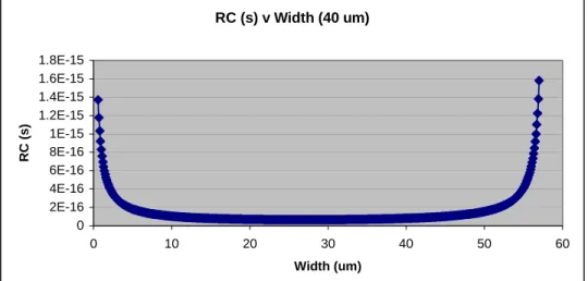
At this point the challenge became determining optimal line sizes. From a variety of simulations it was determined that CPW performance increased as its impedance increased. This is a result of a decrease in capacitance between the signal line and the ground planes as the impedance increases. However, in order to increase the impedance, spacing between the signal line and the ground planes must be increased. At some point, the capacitance between the signal line and its ground planes is minimal compared to the capacitance between the signal line and a conductive plane beneath it. At this point, the line is behaves more like a microstrip than a CPW. An embedded microstrip is modeled by the following: 15 2 ( ) 10 10 937 . 3 8 . 0 98 . 5 ln 41 . 1 1 55 . 1 exp 1 ) ( ) ( − − × × × × × = ⎟ ⎠ ⎞ ⎜ ⎝ ⎛ + = ⎥ ⎦ ⎤ ⎢ ⎣ ⎡ ⎟ ⎠ ⎞ ⎜ ⎝ ⎛ − − = × × = um L C R RC T W H C H H W T L R r o r ε ε ε ρ (3-3) (3-4) (3-5) (3-6) where ρ is the resistivity of the line, ε is the permittivity of the oxide, and εris the relative effective permittivity of the oxide. These equations were used to create the RC curves depicted in Figure 8 [10]. From this curve the maximum signal line width was determined. The minimum RC value is obtained at 27 um. However, in addition to
minimizing the RC of the line, another requirement is to have ground planes of sufficient width. The ground rails need to be approximately four times the width of the signal line in order to prevent their width from effecting the interconnect’s characteristics [9]. They also need to be as wide as possible to prevent crosstalk between signal lines. A
maximum width of 18 um was chosen, since no significant decrease in RC was observed past this value. Table 4 in the results section lists all the line widths and structures chosen, as well as their impedances.
RC (s) v Width (40 um) 0 2E-16 4E-16 6E-16 8E-16 1E-15 1.2E-15 1.4E-15 1.6E-15 1.8E-15 0 10 20 30 40 50 6 Width (um) RC (s) 0
Figure 8: RC curve for 40-um long embedded microstrip with varying widths
3.6 RF Simulations and Verification
Frequency Domain Simulation and Verification
In order to verify that the ADS simulations would accurately predict the
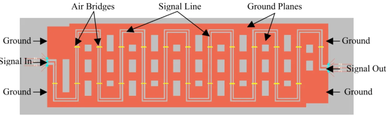
performance of the interconnects within the system, verification with measured data was performed. Figure 9 shows an interconnect structure that was fabricated in MITLL’s 180-nm FDSOI process. The interconnect structure modeled is a CPW with a finite width ground plane.
Signal In Signal Out
Ground Ground
Ground Ground
Air Bridges Signal Line Ground Planes
Figure 9: CPW test structure fabricated in an RF metal stack of Ti:AlSi:Ti:TiN (40 nm : 2000nm :40 nm : 50 nm)
Signal Out Signal In
Ground Ground
Ground Ground
Air Bridges Signal Line Ground Planes
Figure 10: Reproduction of CPW test structure above (Figure 9) for Momentum simulation
The test device was reproduced in ADS’ momentum tool in two ways. First, it was laid out as a straight line with the same characteristic lengths and widths; second it was laid out exactly as it was fabricated, including its serpentine structure. The complete
simulated layout can be seen in Figure 10.
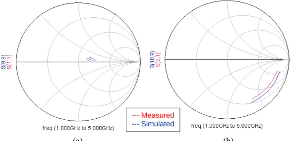
Full electromagnetic frequency domain simulations were run after these two layouts plus substrate parameters were entered into the simulation tool. The simulated data was then plotted in comparison with the measured S-parameter data obtained from the fabricated device. Figure 11 shows a Smith chart with both the simulated
S-parameters from the layout in Figure 10 and the measured S-parameter data. Although the results were not exact, they show that the model is a good conservative estimate of a fabricated structure. Measured resistances attributed to variations caused by RF testing due to probe cables and varying positions of probe tips on the probe pads had values equivalent to the error measured here (~20 Ohms).
--- Measured --- Simulated
(a) (b)
Figure 11: Comparison of measured and simulated S-parameter data; (a) S(1,1); (b) S(2,1)
Time Domain Simulation and Verification
Time domain simulations were also completed. Both the serpentine and straight line models demonstrated the accuracy of the simulation tool. Minor inaccuracies can be attributed to three characteristics of the fabricated structure. These were its finite width ground plane; its serpentine structure; and its change in line width between the probe pads and the CPW line. A CPW test structure with an infinite ground plane, straight path, and better matched impedances between the line and the probe pads would have been a more appropriate structure to model, however a device of this nature was unavailable.
Each model of the fabricated device demonstrated the tool’s accuracy. The straight line matched in amplitude, but not phase (Figure 12a). The phase delay was approximately 10 ps. A phase delay of this magnitude can be attributed to a serpentine structure having a longer effective electrical length. Also increased resistance and capacitance due to bends in the line and airbridges, respectively, could also contribute to the 10 ps delay. Despite this phase delay, the simulated waveform accurately depicted the measured waveform’s amplitude, period and shape.
(a) (b) V Time (ns) V Time (ns) --- Input --- Measured --- Modeled
Figure 12: Time Domain Simulated and Measured Waveforms: (a) measured and straight line simulated waveforms; (b) measured and serpentine line simulated waveforms
The serpentine line matched in phase, but not amplitude (Figure 12b). The simulated waveform had an amplitude that was 77% of the measured amplitude. The simulation tool accurately predicts the delay due to the bends in the structure, but over-estimates their effect on the signal’s amplitude. The phase, period, and shape is
accurately simulated, however, and demonstrates that the simulated waveform of a structure with bends in the line will only provide a conservative estimate of the actual waveform.
All structures simulated for this project are straight lines with at most one T-junction. Consequently any errors present in the simulation due to multiple bends or probing effects would not occur for the system described here. Thus accurate simulation of the H-tree structure can be assumed.
Models
Once verification of the simulation tool was completed, simulation of the structures within the 3D designed system began. The preliminary size and geometry of each interconnect segment was calculated from the MS and CPW models described in Section 3.5. Full electromagnetic models were then created in Momentum for each interconnect branch along the H-tree structure. When performing these simulations the full 3D stack was used as the substrate, so include any effects a 3D structure might have on interconnect performance. A description of the 3D stack is in Section 3.7. Frequently a conductive ground plane is used in interconnect structures. The model assumed a metal plane in the logic tier’s metal 3 resulting from a high density of metal 3, including interconnects and fill.
Simulations using electromagnetic models of the interconnects took hours as opposed to minutes when simple RLC models of the interconnects were used. As a result, it was more time efficient to use an RLC model for an interconnect when performing multiple iterations of the same simulation for transistor sizing. A structure consisting of four resistors, four capacitors, and one inductor (Figure 13) was created for each CPW structure to match the S-parameter data provided by the Momentum simulations. Each
RLC model is a distributed lumped element model with each RLC combination representing a 40-um section of the interconnect.
Figure 13: RLC interconnect model \
C C C C R R R R L
3.7 Three-Dimensional Vias and Stack
During modeling and simulation, the entire 3D stack including both the logic and clock tiers had to be taken into account. As mentioned in Section 3.6, the entire three-dimensional stack was entered into the simulation tool to properly predict performance of these structures within their 3D environment. After three-dimensional integration the final stack exists with the order and thicknesses presented in Table 2 and Figure 14.
The layers consist of a silicon substrate, buried oxide (BOX), Silicon-On-Insulator (SOI), gate oxide (GateOx), Polysilicon gate (Poly), oxide, RF metal (Mtlrf), metal 1 (M1), metal 2 (M2), metal 3 (M3), plasma enhanced tetra-ethyl-ortho-silicate deposited silicon dioxide (PETEOS), and Borosilicate Glass (BSG).
Top of Stack
Bottom of Stack Table 2: Layers in 3D stack and corresponding thicknesses
Top of Stack
Figure 14: 3D stack corresponding
to Table 2 above Bottom of Stack Layer Thk (nm) Layer Thk (nm) BOX 200 PETEOS 1000 PETEOS 1000 BSG 500 BSG 500 BSG 500 BSG 500 PETEOS 1000 PETEOS 1000 M3 630 Mtlrf 2130 Oxide 1000 Oxide 1000 M2 630 M2 630 Oxide 1000 Oxide 1000 M1 630 M1 630 Oxide 600 Oxide 600 Poly 200 Poly 200 GateOx 4 GateOx 4 SOI 40 SOI 40 BOX 200 BOX 200 Silicon 675000 oxide Mtlrf oxide Silicon Handle
The 3D via is an inter-tier feature not listed in the stack. 3D vias are tungsten filled plugs that electrically connect the two closest metal layers of two adjacent tiers. The metal in the top tier has openings that self-align the 3D vias to landing pads in the metal of the bottom tier. A via mask is aligned to the metal in the top tier and the oxide is etched as seen in Figure 15.
Tungsten is deposited by chemical vapor deposition to fill the vias and excess tungsten is removed by chemical-mechanical polishing. An SEM of two 3D vias connecting from Tier 1 to Tier 2 and then from Tier 2 to Tier 3 can be seen in Figure 16. The vias appear to be Y-shaped because the tops of the vias were not entirely filled with tungsten. The resistance of an individual via was determined by the measurement of fabricated via chains. An approximate value of 2 Ohms per via was determined by dividing the total chain resistance by the total number of vias [13].
Figure 15: Cross-section of 3D via
Figure 16: SEM cross-section of two 3D vias
CHAPTER 4 – THREE-DIMENSIONAL FABRICATION
Three-dimensional circuit integration has recently become feasible due to the advantages inherent in an FDSOI fabrication process. These advantages include electric isolation of the 3D vias from the active devices provided by the buried oxide layer; the ability to selectively remove the silicon substrate; and FDSOI is a low-power process that helps reduce the problem of heat dissipation in a 3D stack. MIT Lincoln Laboratory has successfully fabricated an imager comprised of three separately fabricated wafers bonded
into one 3D stack. The process described below is similar to that which was used to create the imager, but tailored to this design.
The process begins with three initial wafers. These can be seen in Figure 17a and consist of a handle wafer, the clock tier, and the logic tier. The two tiers containing active elements, will both be independently processed prior to bonding in the same three-level metal 0.18-um FDSOI CMOS process designed to operate at 1.5 V. To minimize
confusion, the clock tier is defined as Tier 1, and will be the top tier in the final assembly. The logic tier will be referred to as Tier 2.
The 3D process flow for the designed system would proceed as follows and is depicted in Figure 17 [5]. First Tier 1 is inverted, aligned, and bonded to the handle wafer (Figure 17b). The silicon substrate of Tier 1 is then removed (Figure 17c). Tier 2 is then inverted, aligned, and bonded to the backside of Tier 1(Figure 17d). The entire stack is then inverted, causing the substrate of Tier 2 to become the handle silicon for the stack. The original handle wafer is then removed (Figure 17e) and then 3D vias are etched through Tier 1 to Tier 2. The vias are then filled with Tungsten and planarized using chemical-mechanical polishing. The 3D vias electrically connect the top metal of Tier 2 to the bottom metal of Tier 1. The final stack is illustrated in Figure 17f [7].
The typical process flow used at MITLL would not require the initial handle wafer and would simply have the stack with Tier 1 and Tier 2 face to face and the vias would be etched through the back of Tier 2. The reason for the extended process flow was to keep the high speed interconnects as far from the resistive substrate as possible to avoid parasitic capacitance.
Figure 17: 3D Fabrication Process Flow
(A) Two separately fabricated active SOI wafers and an SOI handle wafer
(B) Invert, align, and bond Tier 1 to handle wafer.
(C) Remove silicon substrate from Tier 1
(D) Invert, align, and bond Tier 2 to Tier 1
(E) Invert entire stack, remove handle wafer
(F) Etch 3-D vias, deposit and CMP tungsten interconnect metal
Handle Handle Tier Silicon Tier Silicon Tier Silicon Handle
Tier 1 Silicon Substrate
Handle Silicon Buried Oxide Tier 1 Handle Silicon Buried Oxide Tier 2 Buried Oxide Handle Wafer Handle Silicon
CHAPTER 5 – RESULTS
5.1 Characteristics of the Completed System
The final design was produced by sizing the buffers starting with the final clock driver and its preset load. Table 3 and Table 4 show the sizing and placement of the repeaters and interconnects respectively. The final output waveform at the node can be seen in Figure 18. The characteristics of this waveform and the design goals can be found in Table 5. The final network’s characteristics are well within the design goal range.
Table 3: Transistor widths (um); L = 0.2 um
Buffer Width (um)
pmos1 nmos1 pmos2 nmos2 Final-buffer 18 9 Buffer1 18 9 Buffer2 24 12 Via-driver 36 18 Buffer3 21 18 36 18 Buffer4 36 18 36 18 Buffer 5 35 30 60 30 In-buffer 72 36 72 36
Branch Center Rail (um) Spacing (um) Between
Final-buffer and Buffer1 1; 1 1.05; 1.05 Between Buffer1
and Buffer2 1; 1 1.05; 1.05 Between
Via-driver and Buffer3 12; 6 5; 3 Between Buffer3 and Buffer4 12; 6 5; 3 Between Buffer4 and Buffer 5 18; 9 15; 7.5 Between Buffer5 and In-buffer 18 15
V
Time(ps)
In(V) Out(V)
Figure 18: Final Waveform
Final Waveform Design Goal Rise Time 62 ps ~ 62.5 ps Pulse Width 277s ~ 250 ps
Delay 63 ps N/A
Table 5: Final Network Characteristics
A balanced H-tree distribution network removes all skew due to differing electrical paths, however there is still skew introduced through process variations. Research performed at the Georgia Institute of Technology (Georgia Tech) provided the equations in Table 6 for approximation of internal clock skew due to process variations. Calculations at Georgia Tech were performed on a balanced H-tree network 16 times the size of the network described here and a final value of 62 ps was reported.
Although the exact calculation of skew due to process parameters is outside the scope of this paper, it is apparent from the formulas that the total skew due to process variations is proportional to the internal resistance times the internal capacitance of the network. Considering the system detailed here is of a much smaller size and thus would have proportionately smaller resistances and capacitances, it can be assumed that the
designed system would have a skew equal to a fraction of 62 ps., which was well within the design goal range [3].
Physical Parameter Clock Skew Compact Model
ILD Thickness Variation
⎟⎟ ⎠ ⎞ ⎜⎜ ⎝ ⎛ ⎟⎟ ⎠ ⎞ ⎜⎜ ⎝ ⎛ ∆ − = ILD T ILD T n D c r ILD T CSK T 2 2 2 1 1 2 ) int int ( 4 . 0 ) (
Wire Thickness Variation
⎟⎟ ⎠ ⎞ ⎜⎜ ⎝ ⎛ ⎟⎟ ⎠ ⎞ ⎜⎜ ⎝ ⎛ ∆ − = int int 2 2 2 1 1 2 ) int int ( 4 . 0 ) int ( H H n D c r T CSK T
Threshold Voltage Fluctuation ⎟⎟
⎠ ⎞ ⎜⎜ ⎝ ⎛ ⎟⎟ ⎠ ⎞ ⎜⎜ ⎝ ⎛ ∆ − = t V t V t V DD V t V L C tr R t V CSK T ( ) 0.7
Transistor Channel Length Tolerance
⎟ ⎟ ⎠ ⎞ ⎜ ⎜ ⎝ ⎛∆ = eff L eff L L C tr R eff L CSK T ( ) 0.7
Gate Oxide Thicknesss Tolerance ⎟⎟
⎠ ⎞ ⎜⎜ ⎝ ⎛∆ = ox t ox t L C tr R ox t CSK T ( ) 0.7 IR Drop ⎟⎟ ⎠ ⎞ ⎜⎜ ⎝ ⎛ ⎟⎟ ⎠ ⎞ ⎜⎜ ⎝ ⎛ ∆ − = t V DD V t V DD V DD V L C tr R DD V CSK T ( ) 0.7 Temperature Gradient ⎟ ⎠ ⎞ ⎜ ⎝ ⎛ ⎟ ⎟ ⎟ ⎠ ⎞ ⎜ ⎜ ⎜ ⎝ ⎛ ∆ − + = T T t V DD V t V q g E L C tr R T CSK T ( ) 0.7
Table 6: Clock Skew Components [3]
5.2 Benefits
The overall system was designed to take advantage of the third dimension
area for both active circuitry and the interconnects between them. The additional room can be used to minimize skew, maintain signal integrity, and increase system density.
Skew is decreased by using a balanced distribution network. A balanced network is a network in which any path from the source to a final load is the same including being equal in distance and number of active devices. Balanced networks are usually larger than standard distribution networks for two reasons. First path lengths are longer because they are not direct and they all have to be equal to the longest path length. Second, their regular pattern cannot be routed around active circuitry if the balance is to be maintained. Thus balanced networks are not usually permissible due to spatial limitations placed on the system by the area required for the logical functions of the system. Signal integrity is maintained, if not increased, by having minimal spatial limitation placed on the necessary size and frequency of the repeaters. Larger repeaters with a higher drive current can be used. It also prevents the repeaters from having to be inefficiently distributed as to reduce their interference with the placement of the logical functions. By removing the clock system from the same plane as the logical circuitry, more room is left for additional logical functions in the same area, thus increasing system density. With greater system density, chip size is reduced, which in turn reduces the area across which global signals need to be distributed.
The ability to provide the clock signal to a larger number of registers in the same area, while not having to account for large amounts of clock skew, can allow for a highly desirable increase in clock speed. In addition, good signal integrity improves the
reliability of the signal. Each of these functions in turn can benefit overall system performance and reliability.
CHAPTER 6 - CONCLUSION
This work demonstrates the possible benefits of utilizing three-dimensional circuit integration to overcome the challenges posed by technology scaling and increase system performance. Although the design was all that was necessary for completion of this project, a complete layout of the system was created and will be fabricated in the near future (See Appendices A and B). A preliminary and smaller system is currently in fabrication as well as interconnect test devices that after characterization will provide better models of interconnects in two- and three-dimensions for future designs.
A three-dimensional clock distribution network was designed and simulated. It consists of two tiers with a majority of the clock distribution network on one tier and the logical functions of the system on the other tier. Circuit simulation and analysis indicate the system provides a reduction in global skew, and an increase in clock signal integrity and system density. As a result, an increase in system performance and reliability is expected for the fabricated system.
REFERENCES
[1] “Clock distribution networks in VLSI circuits and systems,” New York: IEEE Press, 1995.
[2] Carloni, L.P. and Sangiovanni-Vincentelli, A.L., “On-Chip Communication Design: Roadblocks and Avenues,” Proc. First IEEE/ACM/IFIP International Conference on Hardware/Software Codesign & System Synthesis, 2003.
[3] Zarkesh-Ha, P.; Mule, T.; Meindl, J.D., “Characterization and modeling of clock skew with process variations,” Proc of the IEEE Custom Integrated Circuits Conference, 1999,pp. 441–444.
[4] Burns, J.; Warner, K.; Gouker, P., “Characterization of fully depleted SOI transistors after removal of the silicon substrate,” IEEE International SOI Conference, 2001, pp. 113-114.
[5] J. Burns et al., “Three-dimensional integrated circuits for low-power,
high-bandwidth systems on a chip” in ISSCC Dig. Tech. Papers, 2001, pp. 268–269. [6] Advanced Design System Documentation 2003A, Agilent Technologies, 2003 [7] Advanced Silicon Technology Group. “MITLL 0.18 µm Low Power FDSOI CMOS
Process Design Guide, version 5.11.” Lexington, MA: MIT Lincoln Laboratory, 2002.
[8] Edwards, T. C., “Foundations of interconnect and microstrip design,” Chichester ; New York: John Wiley, c2000.
[9] Simons, R., “Coplanar waveguide circuits, components, and system,” New York; John Wiley, 2001
[10] IPC-D-317A, Design Guidelines for Electronic Packaging Utilizing High-Speed Techniques, Jan 1995; Section 5, pp. 13 - 36.
[11] Star-Hspice, Version 2002.2, Avant! Corporation, 2002. [12] Quest, Version 2.0.4.R, Silvaco International, 2002.
[13] K. Warner et al., “Low-temperature oxide-bonded three-dimensional integrated circuits” in Proc. IEEE Int. SOI Conf., 2002.
Appendix A: Clock Tier Layout
Appendix B: Logic Tier Layout
Figure B1: Logic Tier’s Local Distribution Network


![Figure 4: Schematic of nmos transistor Figure 5: Multi-fingered nmos transistor with four gate fingers each 6 um wide creating an effective gate width of 24 um [7]](https://thumb-eu.123doks.com/thumbv2/123doknet/14046502.459694/15.918.161.816.125.282/figure-schematic-transistor-figure-fingered-transistor-creating-effective.webp)