Analysis of Mo Sidewall Ohmic Contacts to InGaAs Fins
byDongsung Choi
B.S. Electrical and Computer Engineering
Seoul National University, 2015
Submitted to the Department of Electrical Engineering and Computer Science
in Partial Fulfillment of the Requirements for the Degree of
Master of Science in Electrical Engineering
at the
Massachusetts Institute of Technology
February 2017
MASSACHOSETT ISTUTE OF TECHNOLOGYMAR
13
2017LIBRARIES
ARCHIES
2017 Massachusetts Institute of Technology. All rights reserved.Signature of author
Signature redacted
Deparit/ent of glectrical Engineering and Computer Science January 31, 2017
Certified by
Accepted by
Signature redacted
Jesns A. del Alamo Professor of Electrical Engineering
Thesis Supervisor
Signature redacted
S(
J
Leslie A. KolodziejskiPro essor of Electrical Engineering Chair, Department Committee on Graduate Students
Analysis of Mo Sidewall Ohmic Contacts to InGaAs Fins
byDongsung Choi
Submitted to the Department of Electrical Engineering and Computer Science on January 31, 2017
in Partial Fulfillment of the Requirements for the Degree of Master of Science in Electrical Engineering
Abstract
As transistor size is scaled down, the performance is degraded and many problems, so called short-channel effects, arise. To address this problem, a vertical transistor structure such as vertical nanowire is suggested. In a vertical nanowire field-effect-transistor, the Ohmic contact at the top of the nanowire not only covers the top surface, but also wraps around the sidewall. Because the sidewall is considered to be different from the top surface, it is necessary to study the sidewall Ohmic contact properties such as the contact resistivity.
In this thesis, to explore sidewall contact resistivity, a theoretical model for sidewall contacts is developed. For the suggested test structure, the fin sidewall contact (FSWC) structure, the sidewall contact is modeled with a transmission line model (TLM), and by using TLM, the sidewall contact resistance is derived. Also, an extraction method of the sidewall contact resistivity from the total resistance measured in FSWC structure is developed. Next, process steps to fabricate FSWC structure are developed. FSWC structure is made for Mo/n'-InGaAs contacts. The key step is that the fin etch mask on top of InGaAs is not removed and the metal (Mo) is sputtered so that InGaAs is contacted by the Mo only through the sidewall. Therefore, only a sidewall contact is made without a top contact. Also, to investigate the way to improve the sidewall contact resistivity, the effect of digital etch and annealing on the sidewall contact resistivity is explored.
With the measured total resistance in FSWC structure and the extraction method for sidewall contact resistivity, sidewall contact resistivity for each split of digital etch and annealing are extracted. As a summary of the effect of digital etch and annealing, two cycles of digital etch or sequential annealing up to 400 *C improves the sidewall contact resistivity with little sacrifice in semiconductor resistivity. The best result of sidewall contact resistivity is 3.7+0.01 - im2 at 400 'C annealing, which is about 1.9 times improvement over the non-annealed value,
6.9+0.05 fl. -m 2 but still about 5.4 times larger than the reported top contact resistivity of
0.69+0.3 fl -pm
Thesis supervisor: Jesus A. del Alamo Title: Professor of Electrical Engineering
Acknowledgements
First of all, I would like to thank my thesis advisor, Professor Jesus A. del Alamo, for allowing me to join his group and conducting exciting researches. I am grateful not only for his invaluable advice and guidance in this research, but also for encouraging me when I felt stuck. I could feel his passion and profession for research from the multiple discussions we had. Also, I learned a lot from his meticulous and detailed care for my research and presentations.
I also want to thank Dr. Alon Vardi, who suggested and guided me to dive into this research topic. I learned lots of measurement skills and intuition from him. Also, having a lot of discussions with
him was very helpful for me to explore this topic. I also want to express my gratitude to Xin Zhao, who suggested my original research topic about nanowire contact resistance and taught me many fabrication skills. I can't thank enough Dr. Alon Vardi and Xin Zhao for their patience to my questions, which were tremendous amount.
I appreciate Wenjie Lu for his help and advice. Especially, his welcoming manner and advice at
the beginning of my graduate student life in this group encouraged me a lot and helped me adjust in new environment. I thank Professor Zongyou Yin for his kindness and being my good office mate. Other past or current members of this group including Dr. Donghyun Jin, Dr. Jerome Lin, Dr. Alex Guo, Xiaowei Cai, Shireen Warnock, Yufei Wu, and Ethan Lee always warmly welcomed me and I want to thank them.
My special thanks to my closest friends for their support and our good friendship: Min Sun,
Pin-Chun Shen, Nadim Chowdhury, Jae-one Lee, the same year EECS Korean graduate students and church friends.
Finally, I appreciate my parents and brother's family for their love and support. I cannot fully express my thanks in any words for their wholehearted advice, encouragement, and pray, which have formed my life.
This work was sponsored by DTRA, Lam Research, E3S, and ILJU Academy and Culture Foundation.
Contents
L ist of figures...9
List of tables... 12
CHAPTER 1. Introduction...14
1.1 Emergence of vertical channel transistors...14
1.2 Sidewall contact... 15
1.3 Previous studies... 15
1.4 T hesis outline...16
CHAPTER 2. Theoretical model for fin sidewall contact...17
2.1 Introduction ... 17
2.2 Metal-semiconductor contact and contact resistance...17
2.3 TLM for top contact...19
2.4 TLM for fin sidewall contact ... 24
2.5 Extraction method for sidewall contact resistivity...27
2.5.1 Method for ps extraction...28
2.5.2 Method for Pc extraction...28
2.6 D iscussion... 29
2.7 Sum m ary... 32
CHAPTER 3. Fabrication process...33
3.1 Introduction... 33
3.2 Process flow...33
3.3 Sum m ary... 40
CHAPTER 4. Experimental results and analysis...41
4.1 Introduction... 41
4.2 Measurement results...41
4.3 Parameter extraction...43
4.3.2 ps and Pc extraction... 47
4.4 Effect of digital etch and annealing...55
4.4.1 Effect of digital etch... 55
4.4.2 Effect of annealing...56
4.5 Summary...58
CHAPTER 5. Discussions...59
5.1 Introduction ... 59
5.2 Validity of SCTLM...59
5.3 Negative x-intercept of trend line in R"T vs. - 2xDE---...-.--...62
5.4 The effect of the access line...63
5.5 The assumption about p, for p" extraction...65
5.6 Wf measurement and deadzone extraction...69
5.7 Summary...72
CHAPTER 6. Conclusions and suggestions...74
6.1 Conclusions... 74
List of figures
* Figure 2.1 Band diagrams for contact between metal and n-type semiconductor. (a) Schottky contact (0M > 0s), equilbrium, (b) Ohmic contact (cDm < (s), equilbrium, (c), (d) applying voltage VA to (a) and (b), respectively ((a) and (b) are reproduced from [6], p. 479, and (c) is reproduced from [7], p. 138. Figures are modified by author.)...18 * Figure 2.2 (a) Cross section of contact and channel of transistor (b) Transmission line model for contact (reproduced from [8] and modified by author)...19 * Fgur2.3
If
|Ix)~ vs. ... 20 * Figure 2.4 Rtt W vs. Lcf graph (reproduced from [8] and modified by author)... 21 * Figure 2.5 (a) Prediction of real current flow in the active layer under contact (reproduced from [11] and modified by author), (b) current flow with assumptions in TLM...22 * Figure 2.6 (a) TLM structure of fin with sidewall contacts, (b) TLM for sidewall contact, (c) folded circuit from (b) (superscript 'sw' indicates sidewall contact.)...25 * Figure 2.7 RtotT vs. Lf graph... 261 1
* Figure 2.8 (a) - vs. Wf, (b) 1 2 vs. W...29 Rsw (- R T)
* Figure 2.9 TLM structure with conformal metal around fin...30 * Figure 3.1. Pictorial view of overall process flow...34 * Figure 3.2. Starting heterostructure for FSWC structure...35 * Figure 3.3. Top-down SEM images of central portion of fin (a) before Mo etch, (b) after
* Figure 3.4. Top-down SEM images for a device, especially marked for (a) pad and FSWC structure, (b) FOX protection layer and exposed fin (zoom-in image of FSWC structure in (a)), (c) cartoon for the final FSWC structure...39
* Figure 4.1 Whole FSWC structure including access lines and pads with port
connections... 42
* Figure 4.2. (a) The result of I-V measurement with the first I-V combination and (b) RtotT vs. Lfo for one set of LfO for Lco=1000 nm and Wfo=80 nm in sample SI...43
* Figure 4.3. (a) An example of SEM image for measuring Lf (Lo=750 nm, W = 100 nm,
and Lfo=250 nm in sample Si), (b) Measured Lf for samples (Lo=750 nm), (c) Lf - Lfo vs. Lf0 for each sample (Lo= 750 nm)...45
* Figure 4.4. (a) R"' vs. Wfo sl, (b) Rf" vs. W0s1 for Lc)=1000 nm in sample SI...46
* Figure 4.5. Parallel translation of line for extrapolation in (a) 1/Rs' vs. W and (b) 1/(V 2R " T)z vs. W1 ... 47 * Figure 4.6. (a) An example of SEM image for measuring Wfb (Lco=750 nm, WfO=100 nm, and L10=250 nm), (b) Measured Wfb for the samples (Lco=750 nm), (c) Wfb - Wfo vs. Wfo for each sam ple (Lco= 750 nm )...49
* Figure 4.7. For the devices of Lco=1000 nm in sample S1, (a) plot of equation (4.3) and (b) plot of equation (4.4) ... 50
* Figure 4.8. (a) Definition of Lc with the right half of FSWC structure, (b), (c), (d) three different cases after removing FOX protection layer, (e) thickness of Mo on the sidewall ((Lco, Lfo, Wfo)=(000, 1500, 80) nm in sample Si) (f) Mo overshoot, (g) Mo undercut...52
* Figure 4.9. (a) ps and (b) psW for digital etch spits (S and C indicates Sulfuric acid and
Hydrochloric acid, respectively.)...56
* Figure 4.10. Change of (a) p, and (b) psw as annealing temperature increases...57 * Figure 5.1. (a) SCTLM and (b) two-dimensional resistor mesh model for the FSWC
* Figure 5.2. (a) The fin and the access line in EBL mask for etching the active layer, (b) the boundary of the fin and the access line with metal sidewall contact, (a) and (b) are cross-section at the m iddle of the active layer... 64 * Figure 5.3. Two architectures are suggested to remove current flowing into the access line from the fin before going into the metal contact. (a) Oxide is inserted between the fin and the access line. (b) another architecture allowing current over-spreading...64 * Figure 5.4. (a) Scheme for the contact end resistor measurement (CERM) for TCTLM (reproduced from [17] and modified by the author) (b) scheme 1, (c) scheme 2, and (d) scheme 3 of the modified FSWC for CERM for SCTLM (Nothing is connected to both ends of the fin, and extra contacts at the ends of the fin are just for symmetry (to let current feel perfect symmetry) and not used.)... 67
* Figure 5.5. For the fin of Lco=1000 nm, Wo=80 nm, and Lfo=1500 nm in sample SI, (a) FIB image of cross-section of the fin under the contact, (b) in the channel, (c) top-down SEM image, (d) different fin with top-down SEM image with high-efficiency secondary electron detector, (e) with in-lens detector, (f) parameter definition for calculating fin width at the middle of the InGaAs layer, left figure is modeling of top-down SEM picture for the fin shown in (c)...71
List of tables
* Table 3.1. Splits for FSWC dimension...36
* Table 3.2. Electron charge dose for each fin width...36
* Table 3.3. Summary of digital etch splits and name of samples...37
* Table 4.1 Possible combinations of applying voltage and sensing current (x indicates that the corresponding port is not used for applying or sensing.)...42
* Table 4.2. Comparison of Lf, Lf - Lo, and standard deviation(-) for (Lfo, Lco)=(250, 750), (250, 500) nm in sample S1...46
* Table 4.3. Lf values [nm] that are used for RttT vs. Lf and extraction of Rs" and R sw ... 46
* Table 4.4 W b - WfO and standard deviation (o-)...49
* Table 4.5. Extracted p, and psW from figure 4.7 (a) and (b)...50
* Table 4.6. Result of Lc measurement of sample S3... 54
* Table 4.7 Result of Lc measurement for each sample with dummy devices...55
* Table 4.8 Result of lmo,uc measurement and ALc,wOrst = ALC-MO,UC for each sample...55
* Table 5.1. Used (ps, pcs) [fl - Im, fl - ym2] values in simulation (x indicates Lc >> L" violation.)... 62
* Table 5.2. Extracted Xdc [nm] with RsWT vs. W 0 - 2XDE (X indicates Lc >> Ls' violation. Negative values are marked with bold and italic. Note that because WfO - 2 XDE is not measured value of Wf, Xdc in this table is not real deadzone width.)...63
CHAPTER 1. Introduction
1.1 Emergence of vertical channel transistors
In modem transistors, a major trend has been scaling down the size of the semiconductor device to get advantages such as higher device density and lower supply voltage. But as the device size becomes smaller, lots of problems, in particular short-channel effects, have arisen. For example, because as the channel length becomes shorter, the effect of electric field from source and drain to channel becomes larger. So the control of the gate over the channel decreases and problems such as drain induced barrier lowering (DIBL) and threshold voltage shifting occur. Also, because scaling reduces the distance between metal lines, the overall size of semiconductor device becomes smaller. Consequently, the size of source and drain becomes smaller, so the contact resistance of source and drain becomes larger.
To address these problems, the device foot-print and the direction of transport need to be decoupled, so a vertical channel device was suggested. Because the channel of a vertical channel device is normal to the wafer surface, channel length and device footprint scaling can be separated. So short-channel effects no longer worsen as the foot-print decreases. Another significant advantage of vertical devices is that there is more room for source and drain contacts since they no longer add to the device foot-print. This should result in improved contact resistance over that of the planar device. For vertical channel devices, vertical fin or nanowire field-effect-transistor
(FET) are possible schemes and the latter has been heavily investigated. With the improvement of
subthreshold slope by taking gate-all-around (GAA) structure, vertical nanowire FET is expected to outperform compared with planar fin or nanowire scheme beyond 7 nm node [1]. Recently, there was a report comparing performance of lateral finFET, lateral GAAFET (nanowire FET) and
power and area reduction beyond the 7 nm node. Therefore, vertical channel devices, especially vertical nanowire FETs, are expected to be next generation device scheme due to several advantages such as mitigation of short-channel effects and enough room for source and drain contacts by decoupling channel and foot print direction as well as improvement of subthreshold swing by GAA scheme.
1.2 Sidewall contact
In the investigation of vertical nanowires, the components such as resistance and capacitance that are required for modeling the device with an equivalent circuit model need to be investigated. At first, contact resistance which is one component of device resistance should be tackled. For example, in the vertical nanowire scheme implemented in [2], there are two contacts which are formed at the top and beside the nanowire (source and drain contacts). As the contact in a planar device, the contact beside the nanowire covers the top surface of n'-InGaAs. However, at the top of the nanowire, the metal is not only contacted at the top surface, but also wraps around the sidewall. In both cases of top-down (etch) and bottom-up (growth) approaches for vertical nanowire fabrication, the contact that wraps around the sidewall of the nanowire (sidewall contact) may have different properties such as contact resistivity compared with the contact covering the top surface (top contact). Especially, in top-down approach, the properties of the sidewall contact are expected to be worse than those of the top contact as a result of sidewall damaged by plasma during nanowire etch. Therefore, it is important to investigate the properties of the sidewall contact not only to model it but also to develop processes to optimize it. As the first step, it can be good start to study the way to measure and improve the contact resistivity of the sidewall contact.
1.3 Previous studies
There are some studies about contact resistivity for vertical structures. In [3], contact resistivity of the Ni contact at the top of the nanowire is extracted for bottom-up InAs nanowires. They reported
0.6 fl -pm2 as their best result for contact resistivity with annealing at 300 *C for 1 min. In [4],
two schemes with metal covering only the top surface or both top surface and sidewall of fin structure are studied for Mo/n'-InGaAs contact.
In both studies, contact covering both top surface and sidewall of vertical structure is explored, and they did not distinguish top and sidewall contacts. To investigate sidewall contact, it is needed to develop methods to fabricate a test structure with only sidewall contact. In addition, it is necessary to construct a theoretical model to extract contact resistivity of sidewall contact from the structure.
1.4 Thesis outline
In this thesis, Mo/n'-InGaAs sidewall contacts are investigated. InGaAs is considered as promising material for n-type channel devices [5]. In Chapter 2, a theoretical model for sidewall contact with fin structure is developed. Basics of metal-semiconductor contact and contact resistance is discussed and a transmission line model (TLM) for the top contact is reviewed. Then, TLM for sidewall contact with fin structure is developed and extraction methods for sidewall contact resistivity is described. In Chapter 3, fabrication steps to implement a structure with only sidewall contacts is described. The key point is that, after fin dry etch, the electron beam lithography mask that is used to define the fin is not removed and the metal contact is sputtered so that the active layer is only connected with metal contact at the sidewall. In Chapter 4, experimental results and analysis are presented. For measurements, a four-probe (Kelvin) resistance measurement scheme is used. The results of extraction of the several parameters including contact resistivity are described, and the effect of digital etch and annealing on contact resistivity to improve the contact resistivity is explored. In Chapter 5, several issues are discussed. Finally, in Chapter 6, key points of this study are summarized and several future research topics are suggested.
CHAPTER 2. Theoretical model for fin sidewall contact
2.1 Introduction
In this chapter, we build transmission line model for fin sidewall contact (SCTLM). SCTLM has two contacts on both sides of a fin and can be modified to transmission line model for top contact (TCTLM). Also, we develop extraction method for sidewall contact resistivity, which is used in Chapter 4.
2.2 Metal-semiconductor contact and contact resistance
Depending on the relative magnitude of the work functions for the semiconductor and the metal, there can be two cases of metal-semiconductor contacts: Schottky and Ohmic contact in figure 2.1 (a) and (b), respectively. As depicted in figure 2.1 (c), if the contact is a Schottky contact, when voltage is applied, electron flow is impeded by barrier. As the applied voltage increases, the barrier height decreases, and the current turns out to be exponentially dependent on the forward bias voltage ([6], p. 490). So voltage and current are not linear and it can be considered that the contact resistance is voltage dependent. But as depicted in figure 2.1 (d), if the contact is an Ohmic contact, there is no barrier and the contact resistance does not depend on the applied voltage. In reality, Schottky contact can be used as an Ohmic contact by using semiconductor with high doping at the surface, which makes very narrow Schottky barrier to allow electrons to tunnel through. Basically all contacts in a device need to function as Ohmic contact.
'PH = * - XsKE
Ec
W---
EF Metal n-type semiconductor
(a) e- IM -Ps - qVA (PH Ec E F ... ~ ~ ~ ~ E F S (c) 4M: workfunction of metal s : workfunction of semiconductor Xs : electron affinity of semiconductor VA : applied voltage
q :charge
Ec Metal n-type semiconductor
(b) -e Ec ~i ~---- E FS EFM (d)
Ec : conduction band of semiconductor EF : Fermi level of equilibrium state EFS : quasi Fermi level of semiconductor EFM: quasi Fermi level of metal
Figure 2.1 Band diagrams for contact between metal and n-type semiconductor. (a) Schottky contact ((Dm > 0s), equilbrium, (b) Ohmic contact (Dm < 0s), equilbrium, (c), (d) applying voltage VA to (a) and (b), respectively ((a) and (b) are reproduced from [6], p. 479, and (c) is reproduced from [7], p. 138. Figures are modified by author.).
Even if an Ohmic contact does not have a barrier in the energy band diagram, because the surface is changed from semiconductor to metal, there is a contact resistance as follows:
RC = L(2.1)
where Pc is the contact resistivity which models properties of the contact surface and A is the
normal area to current flow. Equation (2.1) is applied for uniformly flowing current which is normal to cross-section with area A. For planar transistor, current flow direction in channel is perpendicular to that at metal and semiconductor interface, so equation (2.1) is not applicable and current is crowded to one edge of the contact closer to the channel, as shown in figure 2.2 (a). To model a transistor contact, a distributed resistor model, so called transmission line model (TLM), is needed.
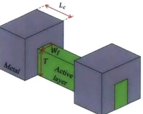
Lc: metal contact length, Lch: channel length, W: metal contact width, T: active layer thickness, ps: semiconductor resistivity of the active layer, pc: contact resistivity for top contact
Metal_-- anel (L) Metal
Current flow Active layer Semiconductor Substrate (a) r--->C dR= -dx --- --- 1B W Ai(&~IdG=- dx dG d V(x)x) I'() = s-A -I 1 --- rj j---- R -S V(0) d R V(x) V(x) sh T +dV(x) 0 x x +dx Lc (b)
Figure 2.2 (a) Cross section of contact and channel of transistor (b) Transmission line model for contact (reproduced from [8] and modified by author).
2.3 TLM for top contact
TLM for top contact (TCTLM) is a distributed resistor model, as shown in figure 2.2 (b). In this model, the metal resistance is ignored and the active layer is assumed to be thin. The differential resistance of the active layer under the metal and the differential conductance across the interface of the metal and the active layer can be modeled as dR and dG, respectively. If appropriate coordinate is set for TLM as depicted in figure 2.2 (b), Kirchoff voltage and current laws can be used at point x as follows [9].
dJ(x) = -V(x)dG = -V(x) dx
PC (2.3)
Superscript 't' refers to top contact. If equations (2.2) and (2.3) are solved with boundary 'conditions, 1(0) = 10 + dI(0) = 10 and I(Lc) = 0, then I(x) and V(x) can be derived. The
results are as follows [9]:
I1(x) = 10 [cosh (it) coth
()sinh(i
(X 1 IO[C A'ot
cosh
sinh(2.4)
(2.5)
where Lt = VptlRh which is called the transfer length. The transfer length can be considered as an effective contact length. It means that considerable amount of current enters contact within x < Lt. The sum of normalized current entering contact within x Lt is as follows.
f dl(X I
10 X-0
fdVx)W
10 PC = cosh(1) - cosh(0) - coth(
T) sinh(1) (2.6)For Lc > Lt , the graph of
[f
dI(x)/1OILI
is as follows.1 0.95 0.9 5. 0.85 ~0.8 0.75 0.7 0.65 0.6 1 2 3 4 5 6 7 LFI Figure 2.3 If |1x jTVS. 8 9 10 .C
If Lc/L >>1, cotangent hyperbolic term becomes nearly unity, then
If
dI(x)/10Ii, convergesto I cosh(1) - cosh(0) - sinh(1)I = 0.63. Therefore, for L, > LT, over 63% of the total current enters contact within x 5 Li., which justifies the name of Lit, 'transfer length'.
By using equation (2.4) and (2.5), the contact resistance of the top contact between points
A and B in figure 2.2 (b) can be derived as follows [9]:
Rt= =() ' coth( ) (2.7)
When Lc >> Li, cotangent hyperbolic term becomes nearly unity and equation (2.7) can be simplified as follows [9].
R =~ w~c (2.8)
From equation (2.8), Rt becomes independent on Lc when Lc
>>
Li. With the structure in figure 2.2 (a), the total resistance (Rtot) from one metal contact to the other metal contact is as follows:Rtot= RCh + 2Rt = TVLCh + 2Rt (2.9) RtOtW Slope: Rt = Ps 2Rh -T 2RtW ich
where RCh = -1 LCh is the resistance of the channel. Several structures such as that of figure 2.2
(a) can be designed with different channel length, and the normalized current, IO/W, can be measured. Then if RtOtW is plotted vs. LCh, then figure 2.4 is obtained. From the slope and
y-intercept of RtOtW vs. LCh, Rt and 2RtW are extracted, respectively. If Lc
>>
Ltr and Rft of the channel is the same as that of the active layer under the metal, the contact resistivity, pc, can be extracted by substituting the value of the slope for Rth in equation (2.8).Although the TLM is a useful tool to model contact resistance, the dimension of the structure needs to be carefully checked to make sure the assumptions are valid. In the TLM, the following two assumptions are made:
1) Because the active semiconductor layer under the metal is modeled with one dimensional
resistance series which is parallel to the metal-active layer interface, it is assumed that there is no vertical voltage drop in the active layer under the metal.
2) Because the TLM includes the semiconductor active layer only under the metal (figure 2.2 (b)), no current over-spreading is assumed (current over-spreading indicates current flux lines which are curved farther than the contact. It is shown in figure 2.5 (a).)
To deal with the first assumption, there is the extended TLM (ETLM), which includes the vertical voltage drop in the semiconductor [10]. Vertical voltage drop is modeled by adding a partial vertical semiconductor resistance of unit area to the contact resistivity as follows:
PC =pct+C-psT (2.10) contact contact --- >-Current over-spreading (a) (b)
Figure 2.5 (a) Prediction of real current flow in the active layer under contact (reproduced from [11] and modified by author), (b) current flow with assumptions in TLM.
where C is a constant which is less than unity and pT is the vertical semiconductor resistance per unit area. The contact resistance in ETLM with LC
>>
L' is obtained by substituting pl* in equation(2.10) for p' in equation (2.8) and the result is as follows:
Rst -pt* Rstf-(pt+C-psT)
* w W = w (2.11)
If a unitless parameter 17 = pc/psT is defined, which indicates the ratio between the contact resistance and the vertical semiconductor resistance per unit area, then equation (2.11) becomes as
follows:
Rc* 'Ri 1+ (2.12)
A reasonable value for C is 0.19 [10]. If an error smaller than 10% is allowed for the TLM
compared with the ETLM, then the following inequality needs to be satisfied.
0.9 -R 1R+t Rt (2.13)
If equation (2.13) is solved for r7, it results in as follows.
r7 > 0.81 (2.14)
If equation (2.14) is rearraged, then
T 1 (2.15)
0.81 Ps
From equation (2.15), in order for the TLM to be applied, the thickness of the active layer needs to be restricted by the ratio between the contact and the semiconductor resistivity.
For the second assumption, to reduce current over-spreading, the contact needs to be sufficiently long. For appropriate criteria of long contact length, Lt can be selected, which indicates the effective contact length. Then the condition, Lc
>>
Li, can be set to reduce current over-spreading. If Lc>>
Lt is rearranged, the following condition comes out.From equation (2.16), like equation (2.15), the condition for small current over-spreading gives, again, a criteria for the dimension of the structure. Combining the two conditions for nj, we have:
0.81 _; 17 « (T (2.17)
Note that the inequality on the left side is derived under the assumption of Lc >> L' which is equivalent to the inequality on the right side.
There can be more assumptions for TLM which can make more conditions other than equation (2.17). Therefore, in practical point of view, it is better to use numerical method. For instance, TLM and two dimensional resistor mesh can be compared via HSpice simulation. From this result, whether TLM is available or not for the fabricated TLM structures can be figured out. However, equation (2.17) is still useful for quick check when we design TLM structures.
2.4 TLM for fin sidewall contact
Sidewall contact is the contact on the sidewall of a vertical structure such as a fin and nanowire. Because sidewall surface of fin and nanowire structure can be different from the as-grown top surface, sidewall contact and top contact need to be considered separately. Because, current flow direction through sidewall contact is perpendicular to that in channel, a distributed resistor network to model the sidewall contact needs to be used. To investigate sidewall contact modeled by distributed resistors, one possible structure is fin structure with sidewall contacts as shown in figure
2.6 (a). TLM for sidewall contact (SCTLM) is shown in figure 2.6 (b). As depicted in figure 2.6
(a), because voltage is applied symmetrically for the axis along the longer side of the active layer, circuit in figure 2.6 (b) is symmetric along the axis. Therefore, the circuit can be folded with the axis and it becomes the circuit shown in figure 2.6 (c). Because the upper and lower dG are connected in parallel, they are combined and become 2dG. If the circuit in figure 2.6 (c) is
compared with TCTLM in figure 2.2 (b), then the circuits become the same if W -> 2T, T -+ Wf/ 2 are applied to TCTLM. R" becomes as follows.
V L Lc Lf (chanel or fin) -- - ---- ---- --dG dl(x4I (x) -- -- --- -- --V(O dR V(x)i V(X) + 14 'C'dV(x) -(a) 0 x x+dx Lc (b) R --- --- B dR T dx G d(x4 (x) dG=Tdx 10 --- ----PG x V(O) dR V(x) V(x) Rw Ps +dV(x) Sh =W1/2 1 1 1) 0 x x + dx Lc (C)
Figure 2.6 (a) TLM structure of fin with sidewall contacts, (b) TLM for sidewall contact, (c) folded circuit from (b) (superscript 'sw' indicates sidewall contact.).
R sh = Ps Ps (2.18)
Wf/2
Here, the superscript 'sw' refers to sidewall contact. Also, from equation (2.7), the resistance between points A and B in figure 2.6 (c) is as follows.
w --Lp (2.19)
cf = coth( s) (.9
where 14W = fprsh. When Lc >> LT, equation (2.19) becomes as follows.
Rsw ~ (2.20)
Actually, the part in black dashed box in figure 2.6 (a) can be seen as a parallel connection of two resistors where one resistor corresponds to the upper half and the second to the lower half. Because parallel connection gives half value of the resistance of a single resistor, this is the reason of one half term on the right hand side of equation (2.19).
RtotT
Slope: !R~' 1 Ps
2R'T-Figure 2.7 RtotT vs. Lf graph.
As we did for the TCTLM, a similar plot to figure 2.4 can be drawn. With the structure in figure 2.6 (a), the total resistance (Rtt) from one contact to the other contact along the fin length is as follows:
Rtot = Rch + 2R W = Lf + 2Rc" (2.21)
where Rch = S L is the resistance of the channel or fin. Several structures depicted in figure 2.6 (a) can be designed with different fin lengths, and the normalized current, I0/T, can be
measured (note that the normalization factor is W for TCTLM, but it is changed to T in SCTLM). Then RtotT can be calculated, which gives figure 2.7 for RtotT vs. Lf. From the slope and y-intercept of Rt0t T vs. Lf, R,', 2R'WT can be extracted, respectively. If Lc >> Lsrw and Rsw of the
channel is the same as that of the active layer under the metal, the contact resistivity, ps", can be extracted by substituting twice of the slope value of RtotT vs. Lf to R,' in equation (2.20). One thing we need to keep in mind is that if W is too wide, then the TLM is not applicable. Thus, if
Wf is changed as a parameter, it would be good to check (rough) available W range by using
equation (2.17) with estimated psw and ps from the literature when the structure is designed.
One interesting point is that the actual current flux can be divided into two kinds: flow into
between R11 and Rx which correspond to I1 and I, respectively. Roughly, R11 and Rx are
proportional to Lf and W, respectively. Because Ix = f+ Ri+R + 1(= 1 1/ 0 where
* +)+(Wf Lf
I is total current, as W1/Lf becomes larger, Ix becomes smaller. If Lf is fixed and W increases,
then, after certain W1, Ix becomes very small and effective W may become saturated. This effect
is expected to be seen easily from the saturation of slope ( R"') in Rtt T vs. Lf graph (figure 2.7). This means that, effectively, the current does not use the whole fin width if W1/Lf is large. (This
is not done in this study and suggested as a future work in Section 6.2.) This two-dimensional effect can be simulated with a two-dimensional resistor mesh in HSpice.
2.5 Extraction method for sidewall contact resistivity
The usual method to extract contact resistivity is as follows. From the y-intercept and slope of Rt0t T vs. Lf in figure 2.7, 2RsWT and 1Rs' can be extracted, respectively. If 2RcsT is rearragned
with the help of equation (2.20) (under the assumption of Lc >> LsT.), pcs can be calculated as
follows.
sw (2R rwT)2
(y-intercept)2 (2.22)
RsW 2xslope
Here, we assume that Rsw of the channel is the same as that of the active layer under the metal contact. However, there is possibility that they are different. According to TCTLM, Rt and RtW do not depend on W1, but, in [4], measurement results show that they depend on W1. The observed W4 dependence of Rt and RtW indicates a non proper current normalization with W. So a 'deadzone' which is a non conductive width from the surface of the fin is introduced. The deadzone width (Xd) is modeled as W -+ Wi - 2Xd and can be extracted from Rt . By using deadzone,
RcWf is corrected to be non dependent on Wf. With consideration of the deadzone, we need to go a step further by considering deadzone in the channel (xdf) and in the active layer under the metal
slope is related to increment of RttT. Here, only channel length is changed for each device (the contact is assumed to be the same for all devices). It indicates that p, and W in R"' from slope of RtOtT vs. Lf graph are totally from channel, not from the active layer under metal contact. However, ps and Wf in R"J[ in RsWT are from the active layer under metal contact. Note that the deadzone can be introduced by W -+ W - 2Xd where
Xd is deadzone width from one side of the
fin. Xd is Xdf and Xdc for Rs' of the channel and RswT, respectively. If Xdf * Xdc (equivalent to Wf - x*f # W - Xdc), or ps in channel # ps in the active layer under the contact, then Rsw of channel # Rsw of the active layer under the contact. In this case, equation (2.22) cannot be used
and another way is needed to extract p!".
2.5.1 Method for p, extraction
Let us assume that we are dealing with only Lc
>>
Lsr' case. Here is the strategy. We assume that ps in the channel and the active layer under metal contacts are the same. (The case that they are different is explained in Section 5.5.) Then, ps can be extracted from Rs' and used to extract psw in 2RswT. If equation (2.18) is rearranged and W -> W - 2XdI is applied, then the following equation comes out.= (W - 2xdf) (2.23)
From equation (2.23), if 1/Rs' vs. W is plotted, then ps and XdI can be extracted from the slope and y (or x)-intercept of the linear extrapolation. An example of a plot of equation (2.23) is shown in figure 2.8 (a). Therefore, from equation (2.23), the semiconductor resistivity of the channel, ps, can be extracted.
1 1 RswA (4-Rf wT)' 2p S 2 Z'/ 2xdacp (a) Wf (b) Wf Figure 2.8 (a) 1 vs. W, (b) 2 vs. W. Rsw (,,f2RswT) 2 (W - 2xdc) (2.24) (V2RswT PsPC
From equation (2.24), 1/pspc' and 2Xdc can be extracted from the slope and y (or x)-intercept of
the linear extrapolation. An example of a plot of equation (2.24) is in figure 2.8 (b). To extract psW
from the slope, we need to assume that p5 for the channel is the same as that for the active layer
under the metal. Then p, which is extracted from 1/Rsw vs. W can be used to extract psW from
the slope of 1/(,v'RcsT)2 vs. W.
From the extrapolation of equation (2.23) and equation (2.24), ps and p1W can be extracted, respectively. In addition, Xdf and Xdc can be extracted simultaneously with p, and pc". So we can
also investigate xdf and Xdc by using these extraction methods. An important point for design is
that to use the extraction methods suggested in figure 2.8, WI needs to be set as variable and devices with different Wf are necessary. Because R,' and RsWT are extracted from Rt0t T vs. Lf,
the total number of devices needs to be # Lf splits x # W splits.
Figure 2.9 TLM structure with conformal metal around fin.
To be more familiar the properties of sidewall contacts, it would be good to compare the sidewall
and top contact resistance. Let us consider a TLM structure with conformal metal around fin shown
in figure 2.9. For simplicity, the contact resistance can be modeled with parallel connection between top and sidewall contact resistance. In this structure, top and sidewall contact resistance can be represented as follows.
Top contact resistance
t__R___p (Le Rc = C cothi-i _1 PSP (__L L
-coth
CW T
I
where RtPs
t t J sh p/Sidewall contact resistance
RcW = 2T coth (Lc) L) PsPcoth 2T I4W'/2 o where Ps ~W/ Lc Ps/( (2.25) SW PC PS / l2)
There are two important points that we need to notice. First, if Lc
>>
LT, Rt oc 1/W and Rsw oc 1/VW. If the active layer is grown by epitaxy, it cannot be too thick. So, there is usually nosmaller, then R' increases faster than Rf". Also, Lt. is not changed as W is scaled. But L"
becomes smaller as WI decreases, and it makes easier to be satisfied with Lc
>>
LT condition. Therefore, Rsw is more robust than R' for WJ scaling. Next, RcW and RsW2T totally depend on properties of top and sidewall contact, respectively. If the current is properly normalized with consideration of the deadzone, the following equations come out from equation (2.25):Rt(W - 2xdc) = -RthIpt coth (Lc) = t coth LC (2.26)
PsL(T-xt)
( T Pc
Rsw2(T - Xdt) = )Rsslpsw coth = (W 2x c)/2 coth LC (2.27)
Ps/(w 2
where Xdt is the deadzone depth from the top surface. Note that because depletion due to Fermi level pinning is one of the possible sources of deadzone, there can also be a deadzone at the top surface. From equation (2.26), Rc(W - 2xdC) depends on pt and Xdt, which are properties of the top contact. Also, from equation (2.27), Rsw2(T - xdt) depends on psW and Xdc, which are properties of the sidewall contact.
Finally, there is one comment on extraction method for ps. If is multiplied on each
Wf121
side of equation (2.23), the result is as follows.
1 = 1 - (2.28)
RSWWf /2 -Rst\ Wj
For equation (2.28), if 1 vs. is plotted, then R t and xdf can be extracted from the slope and y-intercept of the linear extrapolation. This seems more physically meaningful, because multiplying (W/2)/T to Rs' is converting R," to Rt . Because Rth = P can be used to extract
ps, equation (2.28) is another extraction method for parameters. However, equation (2.28) needs
one more modification (multiply ) than equation (2.23) does, so equation (2.23) may give
Wa2
2.7 Summary
In this chapter, we start from basic concept of metal and semiconductor contact and contact resistance. For the top contact, Rt is derived by using TLM and extraction method for Rt and RtW is introduced. Also, two constraints on dimensions of TLM structure for validating assumptions in TLM are evaluated. Next, a structure for sidewall contact is suggested and Rs' for sidewall contact is derived. Extraction of 2Rf"T and Rs' is similar to that of TCTLM. Then
extraction methods for ps and psW are introduced. Finally, properties of Rt and Rf" are compared
and another extraction method for ps is suggested. In the following chapter, fabrication steps for
CHAPTER 3. Fabrication process
3.1 Introduction
In this chapter, we describe the fabrication process for the structure suggested in Chapter 2 to extract sidewall contact resistivity, psw. From now on, this structure is called fin sidewall contact (FSWC) structure. As mentioned in Chapter 2, to extract RfwT and RS', Lf splits are needed. Also, for extraction of ps and pc, W splits are needed. Therefore, a combination of splits for Lf, Wf, andL C are fabricated. To investigate the way to improve pc, digital etch and annealing are explored. For digital etch, there are five splits for combinations of several cycles and chemicals, and each sample corresponds to one digital etch split. For annealing, several temperatures with sequential annealing are tested. Fabrication process is designed and done by Dr. Alon Vardi in Prof. Jesu's A. del Alamo's group.
3.2 Process flow
In this section, the detailed process flow for fabrication of FSWC structure is described. Overall process flow is depicted in figure 3.1. Each step is explained in detail as follows.
Step 1. Starting Heterostructure
Details of the starting heterostructure for FSWC structure is shown in figure 3.2. Each layer is grown by molecular beam epitaxy (MBE) from IntelliEPI Inc. The substrate is semi-insulating InP.
Process description Top view Cross-section view
1. Starting heterostructure
2. Fin writing via electron beam lithography
3. Fin etch by dry etch
4. Digital etch
5. Mo and W deposition
6. Pad formation
7. FOX protection lay electron beam lithography
8. Mo etch
-r writing via
I ISQ
On top of the InP etch stop, there is a highly Si doped (n-3 x 1011cm 3) n'-InxGa1.x,)As cap
composed of two layers: a 30 nm thick layer with x=0.53 followed by a 10 nm thick layer with x=0.7. As mentioned in Chapter 2, to make a good Ohmic contact, a highly doped semiconductor layer is needed at the surface to make a narrow Shottky barrrier. Actually, in our starting heterostructure, the only conductive semiconductor layer is the highly doped cap and this is used as the active layer in the FSWC structure.
n i0 7Ga0As 10 nm Cap (Si- 3 x 1019 cm-3) e' Ine3Ga.4As 30 am Cap (Si~ 3 x 10¹⁹ CM-3)
i Enox~s2A.4s 400 nin Buffer
Figure 3.2. Starting heterostructure for FSWC structure.
Step 2. Fin writing via electron beam lithography
The process starts by cleaving the wafers as received from the grower in five pieces (about 1 cm x 1 cm size). They are then cleaned in acetone with ultrasonic for 3 min to remove particles on the surface of the samples. About a 2-3 nm Si3N4 adhesion layer is deposited to facilitate adhesion of hydrogen silsesquioxane (HSQ) through chemical vapor deposition (CVD) in an STS/Multiplex
PECVD. High frequency deposition (13.56 MHz on showerhead) is used. For wide area pattern, HSQ does not need an adhesion layer to be patterned on an InGaAs surface, but an adhesion layer
is necessary for HSQ for small area or narrow patterns. Results of HSQ adhesion tests with evaporated thin Si layer as an adhesion layer are shown in [12]. Si3N4 is used instead of Si in this
study. After adhesion layer deposition, 6% HSQ is spun on samples in spin coater at 3500 rpm for 1 min. Then fin writing is done via electron beam lithography (EBL) using an Elionix ELS-F 125. Acceleration voltage of electron beam, writing resolution, and current are 125 keV, 2 nm, and 1 nA, respectively. Leo, Lfo, and Wfo (written value of Lc, Lf, and W4 via electron beam lithography, respectively) are shown in table 3.1. In Chapter 5 (after p'w is extracted in Chapter 4), whether
is derived in Chapter 2 as well as numerical method using HSpice. Because different sized patterns need a different electron charge dose, from dose test of HSQ, a dose for each width of the fin is determined as summarized in table 3.2. After EBL, HSQ is developed with 25% tetramethylammonium hydroxide (TMAH) for 72 sec. Then the samples are rinsed with acetone, methanol and isopropyl alcohol.
Table 3.1. Splits for FSWC dimension.
Dimension Splits [nm]
Lc 500,750,1000
Lf 250, 500, 750, 1000, 1250, 1500
Wf 40, 50, 60, 70, 80, 90, 100, 200
Table 3.2. Electron charge dose for each fin width.
WIfo [nm] Dose [MC/cm2
]
40-60 6400
70-100 6075
200 5200
Step 3. Fin etch by dry etch
For the next step, the fin structure is etched through inductively coupled plasma reactive ion etch
(ICP RIE) in SAMCO 200iP. After cleaning and conditioning the chamber, InGaAs and InAlAs
are etched for 80 sec with BCl3/SiCl4/Ar of gas flow 3/0.53/11 sccm, respectively. This recipe is
developed for highly anisotropic InGaAs etch for high aspect ratio vertical structure [13]. Step 4. Digital etch
After the fin etch is done, digital etch is applied for each sample. Digital etch is composed of two steps: self-limited oxidation with oxygen plasma and wet etch with acid solution. Oxidation step is done with oxygen plasma in Asher for 3 min and the applied power is 1000 W. After oxidation steps, wet etch is done for 1 min with the first cycle and 10 sec after the second cycle. Chemicals for wet etch are H2SO4 (H2SO4:H20=l:1) or HCI (HCl:H20=1 :3). For the H2SO4 solution, right
heat during digital etch, enough cooling down of solution is necessary. Typically, single cycle of digital etch removes I nm [14]. The purpose of digital etch is removing a surface layer which is damaged by plasma during fin etch and in this way exposing a higher quality surface. In this study, to investigate the way to improve p", the number of digital etch cycles and two kinds of acids for wet etch are explored for each sample. Table 3.3 gives the nomenclature of the samples, which indicates the digital etch splits.
Table 3.3. Summary of digital etch splits and name of samples.
Digital etch cycles 1 cycle 2 cycle 3 cycle
H2SO4 Si S2 S3
HCl C1 C2
Step 5. Mo and W deposition
After digital etch, 50 nm of Molybdenum (Mo) and 10 nm of Tungsten (W) are sputtered in an
AJA International ATC- 1800. Mo and W need to be sputtered right after the samples are
wet-etched, because native oxide is produced by exposing the sample to air yielding a worse contact. The reason for using W is to prevent Mo from oxidation [15]. Note that HSQ fin mask on top of InGaAs is not removed. This insures that, after Mo and W deposition, the active layer is only contacted with Mo on the sidewalls. This is the key point of making sidewall contact without top contact.
Step 6. Pad formation
After Mo and W deposition, pads are formed through lift-off using photo lithography. AZ5214-E, an image reversal photoresist, is spun on the samples in a spin coater for 30 sec at 3000 rpm. The samples are pre-baked on a hotplate for 2 min at 80 *C. Then the samples are aligned and exposed to UV in a Karl Suss MA6 contact aligner, for 9 sec with low vacuum condition. Because the photoresist needs to be reversed, the samples are baked on a hotplate for 80 sec at 110 *C. Then, for flood exposure, the samples are exposed to UV again for 90 sec. After this, the photoresist is developed by using AZ422 for 120 sec. Then 15 nm Ti is deposited followed by 75 nm Au deposition with electron beam evaporation in a Temescal VES2550. Finally, the pads are formed through lift-off by dipping the samples in acetone.
Step 7. FOX protection layer writing via electron beam lithography
To isolate devices from each other, Mo and W need to be etched. Because Mo and W under the pads are protected by the Au pad during Mo and W etch, a protection layer for the access line from the pads to the active device is needed. For the protection layer, FOX 16 (high concentration HSQ from Dow Coming) is used. FOX is spun on the samples with 3000 rpm for I min in spin coater. Then the pattern for the protection layer is written via EBL in the Elionix ELS-F 125. Acceleration voltage, writing resolution, and current are 125 keV, 5 nm, and 10 nA, respectively. 1548 and 1400 PC/cm2 are used for electron dose of Lfo= 250 nm and other Lfo, respectively. After EBL, FOX is developed with 25% TMAH for 90 sec. In this process, Wfo nm in the central portion of the fin should not be covered by FOX, because it is the channel of the FSWC structure, and Mo and W that cover it need to be etched.
Step 8. Mo and W etch
After the FOX protection layer is made, Mo and W are etched with SF6/02 with a gas flow 87/10
sccm, respectively, via electron cyclotron resonance reactive ion etching (ECR RIE) in Plasmaquest Series 11 Model 145. Etching time is 160 sec with around 10 sec overetch. Mo and W on the central portion of the fin are etched and the device is isolated. Actually, the fins are not completely vertical, Mo and W on the sidewall are also etched. Mo and W under the FOX
(a) (b)
Figure 3.3. Top-down SEM images of central portion of fin (a) before Mo etch, (b) after Mo etch. protection layer and the Au pads are not etched. Top-down images taken by scanning electron
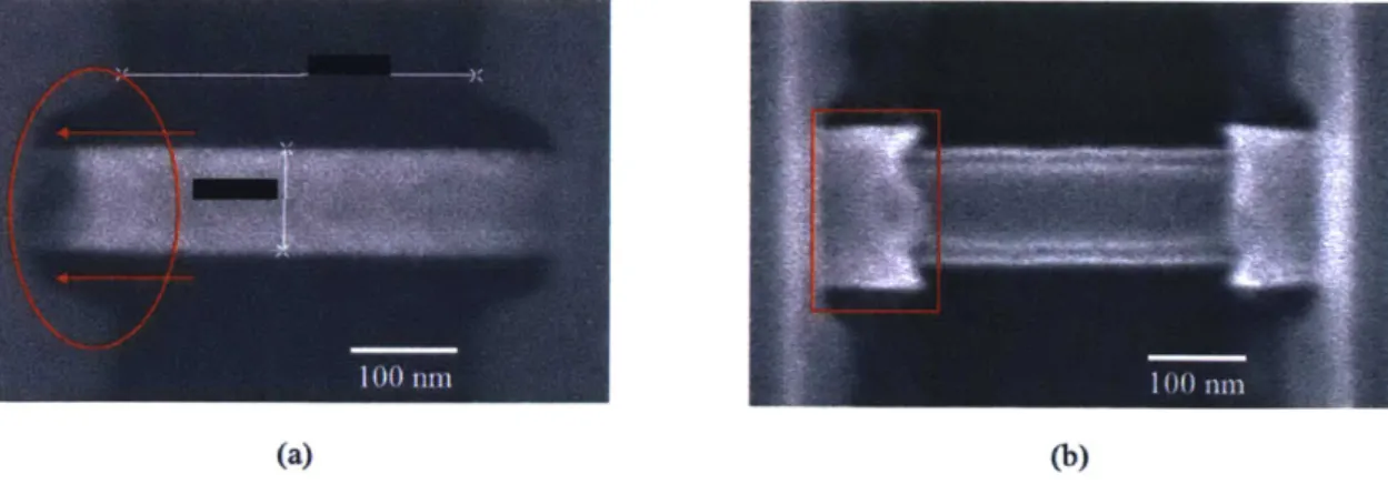
3.3 (a) and (b), it is clearly seen that, after Mo and W etch, the exposed semiconductor fin has a
width that is narrower than that of the fin covered by Mo and W. Actually, on top of the semiconductor fin, there is an HSQ fin mask. Although the HSQ is etched by SF6, in Chapter 4, through focused ion beam (FIB) image, we confirm that not all HSQ fin mask is etched by Mo and W overetch. Also, the reason of tilted entrance of FOX tunnel at the both ends of the fin (one end of the fin is marked with red circle and arrows in figure 3.3 (a), also seen in figure 3.3 (b)) is because FOX goes back when SEM is zoomed in. The reason for this behavior of the FOX layer is not clear at this moment, but one possible explanation is damaging of FOX because of electron beam. Actually, in figure 3.3 (b), Mo and W part at both ends of the fin should be covered with FOX and supposed not to be inspected via top-down view. But because FOX goes back after zoom in, Mo and W part (marked with red squares in figure 3.3 (b)) is revealed and can be inspected. Top-down SEM images of the final device are shown in figure 3.4 (a) and (b). Also, in figure 3.4 (c), a cartoon for the final FSWC structure is shown.
Pad . FSWC (a) (b) =MO & W SHSQ m In~mAs MInAlAs (W
Figure 3.4. Top-down SEM images for a device, especially marked for (a) pad and FSWC structure, (b)
FOX protection layer and exposed fin (zoom-in image of FSWC structure in (a)), (c) cartoon for the final FSWC structure.
Step 9. Annealing
As mentioned at the beginning, annealing is another factor that is investigated to improve pIW in this study. Annealing is done only for sample CI through rapid-thermal annealing (RTA) in N2
ambient in an Annealsys reactor. Annealing temperatures are 250, 300, 350, and 400 *C, and the sample is sequentially annealed for 3 min at each temperature. At 400 *C, to prevent decomposition of InGaAs, the sample is upside down on a GaAs piece.
3.3 Summary
In this chapter, each step of the process flow for FSWC structure is described. The key point of the process is sputtering Mo and W with HSQ fin mask on top of the active layer. Therefore, there is no top contact, but only sidewall contact between the active layer and Mo, which is the same structure as that suggested in Chapter 2. In the next chapter, measurement results and analysis will be described.
CHAPTER 4. Experimental results and analysis
4.1 Introduction
In this chapter, we describe measurement results and analyze them. First, the measurement method, four probe Kelvin technique, is explained and results of I-V measurements of the FSWC structure as well as R totT vs. Lf are displayed. Next, the result of extraction of R"', RswT, ps, and p" are given. Then, the impact of digital etch and annealing on p" is described.
4.2 Measurement results
I-V measurements are done for the FSWC structures which are fabricated in Chapter 2. For this measurement, the four-probe (Kelvin) resistance measurement scheme is used. Because Kelvin resistance measurement scheme measures current and voltage from different probes, the resistance of the cable connecting the probe and test station does not affect the measurements. In figure 4.1, the whole FSWC structure including the access line and the pads with port connections is shown. Among the four ports, one port is used for applying and sweeping voltage, and measuring the current. Another one pair of ports is used for sensing voltage. If symmetry with the axes along the longer and shorter sides of the fin (axis 1 and axis s in figure 4.1, respectively) is considered, there are four possible combinations of applying voltage and sensing current, and they are shown in table 4.1. In figure 4.1, the pads which are touched by port 1 and 3 are connected via metal access lines. Because (if we ignore resistance of metal) every point on the metal access line from port 1 and 3 has the same potential, port 1 and 3 are, effectively, applied to the same end of fin.
Port 3 -Fin Access line Axis 1 ---Pad Port 1 Port 2
Figure 4.1 Whole FSWC structure including access lines and pads with port connections. Table 4.1 Possible combinations of applying voltage and sensing current ( x
corresponding port is not used for applying or sensing.).
indicates that the
I-V Combination Port 1 Port 2 Port 3 Port 4
Apply Vapp (sweep) V = 0 1 = 0 1 = 0
Sense I x V V2
2 Apply Vapp (sweep) I = 0 1 = 0 V = 0
Sense I V2 V1 x
3 Apply I = 0 V = 0 Vapp (sweep) I = 0
Sense V1 x I V2
4 Apply I = 0 1 = 0 Vapp (sweep) V = 0
Sense V1 V2 I x
This means that changing ports 1 and 3 does not affect the result. This argument can also be applied to ports 2 and 4. Therefore, all V combinations in table 4.1 should give the same V results. V measurements are done with Agilent 4155A semiconductor paramter analyzer. The result of I-V measurements for the first I-I-V combination for one set of Lo devices with Lco=1000 nm and
Wo=80 nm in sample SI are shown in figure 4.2 (a). The horizontal axis of the graph in figure 4.2
(a) is V1-V2 which, in principle, is the same as the applied voltage, Vapp. The vertical axis of the
graph is the normalized current by the thickness of the active layer (T=40 nm). The reason why normalization factor is thickness of the active layer is described in Chapter. 2. The result shown in

![Figure 2.4 RtOtW vs. Lch graph (reproduced from [8] and modified by author).](https://thumb-eu.123doks.com/thumbv2/123doknet/14172078.474751/21.917.247.620.609.989/figure-rtotw-vs-lch-graph-reproduced-modified-author.webp)
![Figure 2.5 (a) Prediction of real current flow in the active layer under contact (reproduced from [11] and modified by author), (b) current flow with assumptions in TLM.](https://thumb-eu.123doks.com/thumbv2/123doknet/14172078.474751/22.917.232.669.816.954/figure-prediction-current-contact-reproduced-modified-current-assumptions.webp)