HAL Id: cea-01846952
https://hal-cea.archives-ouvertes.fr/cea-01846952
Submitted on 10 Jan 2019
HAL is a multi-disciplinary open access
archive for the deposit and dissemination of
sci-entific research documents, whether they are
pub-lished or not. The documents may come from
teaching and research institutions in France or
abroad, or from public or private research centers.
L’archive ouverte pluridisciplinaire HAL, est
destinée au dépôt et à la diffusion de documents
scientifiques de niveau recherche, publiés ou non,
émanant des établissements d’enseignement et de
recherche français ou étrangers, des laboratoires
publics ou privés.
Heteroepitaxial diamond on iridium: New insights on
domain formation
N. Vaissiere, S. Saada, M. Bouttemy, A. Etcheberry, P. Bergonzo,
Jean-Charles Arnault
To cite this version:
N. Vaissiere, S. Saada, M. Bouttemy, A. Etcheberry, P. Bergonzo, et al.. Heteroepitaxial diamond
on iridium: New insights on domain formation. Diamond and Related Materials, Elsevier, 2013, 36,
pp.16 - 25. �10.1016/j.diamond.2013.03.010�. �cea-01846952�
Heteroepitaxial diamond on iridium: New insights on domain formation
N.
Vaissiere
a,⁎
,
S. Saada
a,
M. Bouttemy
b,
A. Etcheberry
b,
P. Bergonzo
a,
J.C. Arnault
aa CEA, LIST, Diamond Sensors Laboratory, F-91191 Gif sur Yvette, France
b Institut Lavoisier de Versailles, UMR 8180, Université de Versailles Saint-Quentin en Yvelines, 45 Avenue des Etats-Unis, 78000 Versailles, France
Topography and chemical evolutions of the iridium surface in the successive steps of bias-enhanced nucle-ation and growth were investigated using scanning electron microscopy (SEM), atomic force microscopy (AFM), and nano-Auger analyses. This sequential approach, which was performed in localized areas at the nanoscale, provides three new experimental and complementary concepts that can enhance the knowledge of nucleation pathways on iridium. First, SEM imaging at low-acceleration voltage enables the detection of diamond nuclei or stable precursors after the BEN step. Second, domains consist of iridium furrows that are covered by an amorphous carbon overlayer, with a thickness of 6.8 nm, according to AFM and X-ray photo-emission spectroscopy data. Third, SEM observations also suggest a close relationship between furrows created under ion bombardment and domains in our study conditions. These results prompted us to propose a scheme that describes the topography and surface chemistry of domains.
1. Introduction
Compared with other heterosubstrates (Si, 3C-SiC), the nucleation mechanism of diamond on iridium appears to be a unique pathway. This mechanism involves the formation of domains[1,2]that are pro-duced during bias-enhanced nucleation (BEN). For these particular areas, epitaxial diamond is obtained after CVD growth. However, in contrast to observations on silicon or silicon carbide, observations on diamond crystal are not possible prior to the growth step. This suggests that diamond nuclei are somehow protected from the CVD plasma during the BEN step. A pseudo-2D growth mode was subse-quently reported during the growth step[3,4]. This finding may ex-plain the higher crystalline quality of the epitaxial diamond layers that were grown on iridium[1,5,6]. Previous studies have demon-strated that surface modifications of iridium simultaneously occur during BEN, namely, roughening[5,7–9]or carbon dissolution[10].
Several important questions remain regarding this particular nu-cleation pathway that occurs on Ir: Does surface roughening play a role in domain formation? Would it be possible to detect diamond nuclei prior to growth using SEM? What are the topography and sur-face chemistry of domains? This study combines two experimental approaches: first, an investigation of the evolution of surface mor-phology during the nucleation process was performed in the same localized areas at the nanoscale (SEM and AFM); second, the surface chemistry was probed within the domains using nano-Auger. New ex-perimental findings are reported concerning the localization of nuclei
after the BEN step, such as the role of furrows in domain formation. The topography and surface chemistry of domains were also examined. 2. Experimental
2.1. Iridium/STO samples
Iridium buffer layers with thicknesses of 200 nm were grown at 900 °C by e-beam evaporation (M-EV) on single crystals of SrTiO3
(001), which were purchased from CrysTec Inc. The iridium deposi-tion rate was 2 nm per min under a pressure of 9.0 × 10− 7mbar.
The full widths at half maximum (FWHM) of the rocking curve (ω-scan) and the azimuthal curve (ϕ-scan) for the Ir(200) and Ir(220) peaks were measured by X-ray diffraction, are 0.22° and 0.26°, respectively.
2.2. BEN and growth
The Ir/SrTiO3(001) substrates (5 × 5 mm2) were transferred to a
microwave plasma-enhanced chemical vapor deposition (MPCVD) reactor, which was equipped with a 2 kW SAIREM microwave gener-ator that operated at 2.45 GHz. This reactor was connected to an ultra-high vacuum (UHV) Omicron system for surface sequential analysis. The base pressure of the reactor was 10− 9mbar and gases
of high-purity research grades were employed: N55 for methane and N90 for hydrogen (a catalytic purifier is present on the gas line). The substrate holder was electrically insulated from the metallic walls of the reactor, which were maintained at ground potential; thus, it was possible to apply a negative voltage to the substrate holder during plasma exposition.
⁎ Corresponding author.
To induce diamond epitaxial nucleation on the iridium surface, the BEN step was applied. As previously detailed[11], the entire nucle-ation process consists of three successive steps: (i) a pure hydrogen plasma is applied to clean the surface; (ii) a methane/hydrogen plas-ma exposure enables stabilization of the sample temperature; and (iii) the BEN treatment occurs, with a duration of 30 or 60 min. During the BEN step, a negative bias voltage of −307 V was applied between
the sample holder and the walls. At the end of the BEN step, the plas-ma exposition and the bias voltage were stopped simultaneously.
A growth step with a duration of either 5 or 15 min was applied to reveal the diamond nanocrystals. The sample was cooled under a secondary vacuum after growth, without the presence of plasma and process gases. The nucleation process and growth experimental parameters are listed inTable 1.
2.3. SEM and AFM investigations of surface topography
The surface topography was observed by field emission scanning electron microscopy (FE-SEM) performed with a Zeiss Supra 40 mi-croscope. By using an in-lens detector, a high lateral resolution of approximately 3 nm was obtained. Pictures were recorded for two acceleration voltages of the incident primary electron beam (20 kV and 0.5 kV). A localization technique, which consists of observing an area on a nanometric scale prior to the MPCVD process and imaging the same area after plasma exposure, was developed for SEM obser-vations. By maintaining a constant brightness, contrast and working Table 1
Experimental CVD parameters for the nucleation process and growth. τCH4= [CH4] /
([CH4] + [H2]) corresponds to the mole fraction of methane in the reactor.
Steps Nucleation process Growth
H2cleaning H2/CH4stabilization BEN Short/long
τCH4(%) 0 4 4 0.6 Pressure (mbar) 20 20 20 20 Power (W) 400 400 400 400 U (V) 0 0 − 307 0 T (°C) 650 650 700/750 650/700 t (min) 10 10 30/60 5/15
Fig 1. SEM images and XPS spectra of iridium surface after each step: (a) as received, (b) after H2cleaning and (c) after H2/CH4stabilization. The two XPS C1s spectra recorded after
distance during the SEM analyses regardless of the voltage, an image treatment was applied on the SEM images to accurately compare the gray level distributions. Threshold tools were employed to associate specific colors with some of the gray levels observed after the nucle-ation process and short growth period. To enhance the image contrast, an FFT bandpass filter was applied prior to an autoscale gray level using the ImageJ software. The FFT bandpass filter adjusts large struc-tures (shading correction) and small strucstruc-tures (smoothing) through Gaussian filtering in Fourier space.
The surface topography of the samples was also investigated by AFM (Molecular Imaging PicoLE), which was operated in non-contact mode. 2.4. Surface chemistry
The first two steps of the nucleation process were previously ana-lyzed by XPS [10]. The main results are summarized in part 3.1. Assuming a homogeneous layer, the XPS data were used to extract an equivalent thickness for the carbon overlayer that was detected on iridium after the BEN step [10,11]. Complementary nano-AES spectroscopy is currently used to investigate the chemistry of specific areas on a localized scale. Auger spectroscopy is extremely sensitive to the carbon-binding state because two valence electrons are in-volved in the C KVV transition. Surface analyses were achieved using the JEOL Jamp 9500F, which is a new generation of Auger nanoprobe. The following optimized conditions were employed: ac-celeration voltage of 10 kV; beam current of 5 nA (lateral resolution equivalent to a spot size of 15 nm), and tilt of 40°. The energy
resolution was dE / E = 0.5% at 2000 eV. Wide scans were acquired with a 50 ms dwell time and an energy step of 0.25 eV. The resolution of the elemental maps and the positioning stability of the scanned area were controlled using a probe-tracking control tool. For Auger references, a single-crystal diamond was cleaned using an acid and plasma hydrogenation pre-treatment to eliminate or minimize the inherent carbon contamination. Concerning the HOPG sample, a fresh surface was produced by cleavage using a tape. Wide-scan AES spectra (not presented in this study) revealed the absence of O-KLL signals, which indicated that neither surfaces exhibited oxygen and carbon contamination.
3. Results
During the successive steps of the process (cleaning with pure hydrogen plasma, stabilization under CH4/H2plasma and BEN), the
surface evolves morphologically and chemically. A sequential SEM study was performed on the same localized areas on a nanometric scale. First, the surface evolution (prior to BEN) during the stabiliza-tion step is presented (part3.1). Second, the effects induced by the BEN step (parts3.2, 3.3, and 3.4) are discussed. Last, a short growth step, which was applied to reveal heteroepitaxial diamond crystals, is examined (part3.7).
3.1. Morphology and surface chemistry evolution of iridium before BEN
Fig. 1shows the SEM images of the iridium surface for the two steps preceding BEN: after H2plasma and after H2/CH4plasma. The
image contrast was enhanced by an FFT bandpass filter and an autoscale gray level using ImageJ software. SEM revealed a granular morphology with oxygen and carbon surface contaminations of 2.5 and 33.0 at.%, respectively, on the initial iridium surface, as revealed by XPS (Fig. 1a). The H2plasma causes an efficient surface cleaning
of initial carbon and oxygen contaminations, as evidenced by XPS (Fig. 1b). These concentrations are below the detection limit (0.5 at.%)
[10,12]. Similar granular morphology is evident after H2 plasma
(Fig. 1b). A loss of granular morphology is observed after H2/CH4with
a surface softening in the same area. Previous XPS investigations revealed the presence of a carbon overlayer with an equivalent thick-ness of 1.4 nm[10].Fig. 1c provides a comparison of the XPS spectra that was recorded in the 280–305 eV binding energy range before and after H2/CH4plasma. The formation of this carbon layer is most likely
due to segregation during the cooling of carbon solubilized at high temperatures in the iridium, as previously shown[10]. The XPS results demonstrate that the iridium surface is most likely free from any carbon overlayer once the BEN begins directly after the stabilization step. SEM observations in the same area indicate that there is no evolution of surface morphology, with the exception of a smoothening of the sur-face. According to SEM and XPS experiments, no trace of diamond was detected on the surface at this stage.
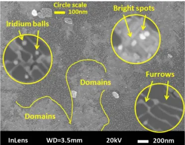
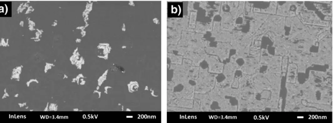
Fig. 2. SEM image of iridium surface after the BEN step. The scale of the images inside the circles is 100 nm.
3.2. Surface morphological changes induced by the BEN step
The BEN step leads to significant changes in surface morpholo-gy, as illustrated in Fig. 2. Different nanosized structures are observed on the iridium surface. The SEM image reveals white spots, iridium balls (spherical nanoislands), and furrows, as well as various contrasts that are named domains[8]. All surface modi-fications are associated with ion bombardment that was induced by the bias.
Among these structures, the domains are located at the origin of the heteroepitaxial diamond growth, as shown inFig. 3and in accor-dance with the literature[6].
3.3. SEM investigation of domains
A SEM study was conducted using the localization area technique and the sequential approach of the MPCVD process. This sequential approach was conducted in parallel using two acceleration voltages: 20 kV was utilized to enhance the lateral resolution because the
outlines of the domains are very thin, and a low acceleration voltage of 0.5 kV was employed to enhance surface sensitivity.
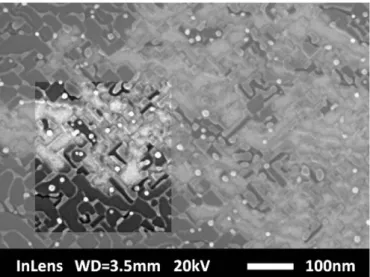
After the BEN step, homogeneous bright areas corresponding to domains were observed in the surface image at 20 kV, as shown in
Fig. 4a. Image treatment was performed to isolate these bright areas and obtain a better observation. First, a threshold was applied on the grayscale to select furrows and domains. Second, furrows were separated from domains based on size and shape criteria. Third, a red layer mask was used to color the domains.
After a short growth step of 5 min, the corresponding new gray level displays a green color. This image analysis is displayed in
Fig. 4b. The green areas are confined to locations that previously contained domains. No morphological modifications are present on the iridium surface: furrows and iridium balls do not appear to evolve. At a very low acceleration voltage (0.5 kV), another area was observed on the same sample after the BEN step, in which a heteroge-neous contrast appears inside the domains: bright spots appear inside the red domains. The same treatment that was previously applied is used to distinguish the blue domains, as shown inFig. 4c.
Fig. 4. Two areas observed after 30 min of BEN (first line) and after a short CVD growth of 5 min (second line) by FEG–SEM at different acceleration voltages: 20 kV for (a) and (b), 0.5 kV for (c) and (d), respectively.
After a short growth step of 5 min and after the image treatment, two characteristic gray level ranges were discernible, as shown in
Fig. 4d, namely, the presence of domains (colored red) and the ap-pearance of green spots. A distinct similarity was detected between the heterogeneities observed after the BEN step, which appear blue inFig. 4c, and the location of the green areas after the short growth, as illustrated inFig. 4d.
Considering that domains lead to the formation of heteroepitaxial diamond, we can assume that these green areas correspond to the presence of diamond nanocrystals after this short growth step. Concerning the blue spots after the BEN step, the presence of some novel precursors or diamond nuclei, which appear prior to the growth step, should be considered.
3.4. Furrows
SEM observations also highlight the presence of furrows on the iridium surface just after the BEN step (Fig. 2). The topography of these surface patterns is dependent on the plasma parameters, namely, the carbon concentration and the bias voltage, as previously reported in the literature[5,13]. However, the furrows do not evolve during the growth step. Their morphology also changes with the du-ration of BEN.Fig. 5shows that the different shapes of these iridium structures are predominantly oriented in the [100] and [010] direc-tions, as shown inFigs. 7aand8 [6,11].
Due to the contrast adjustment inFig. 6, furrows are visible within the domains. According to our SEM statistical observations, no do-main was observed without furrows. So, furrows are likely to be re-quired to form domains on the iridium surface.
After the BEN step, a 15 min growth step confirms the formation of heteroepitaxial diamond within the domains in which furrows
are present. Furrows remain at the surface without morphological modifications after the growth step. Subsequently, diamond crystals grow at 45° with respect to the direction of the furrows, as shown inFig. 7b.
3.5. Temporal evolution of domain formation
The temporal evolution of the domains was investigated by SEM (Fig. 8). For two samples which underwent the BEN steps for 30 and 60 min, the coverage of the iridium surface by domains increased from 8% to 86%, respectively.
This observation suggests that two possible schemes are crucial to domain expansion. First, the nucleation of new domains may occur during the BEN step. Second, domains may grow by propagation mechanisms, which may lead to expansion and coalescence. The temporal evolution of domains may be a combination of these two phenomena that occur during the BEN step.
The domain expansion is limited by the topography of the iridium surface, namely, by the steps between terraces (appearing as dark lines inFig. 8b). This occurrence prevents total coverage of the surface by domains.
As observed in the SEM images (Fig. 9), a high magnification of these dense domains after 60 min of the BEN step reveals structures that resemble cubic nanoislands.
As described in part3.4, furrows are present all over the iridium surface, namely, within domains; they exhibit a temporal evolution during BEN. These cubic forms are associated with the roughening of the iridium surface, which produces other furrow shapes. 3.6. Topography of dense domains
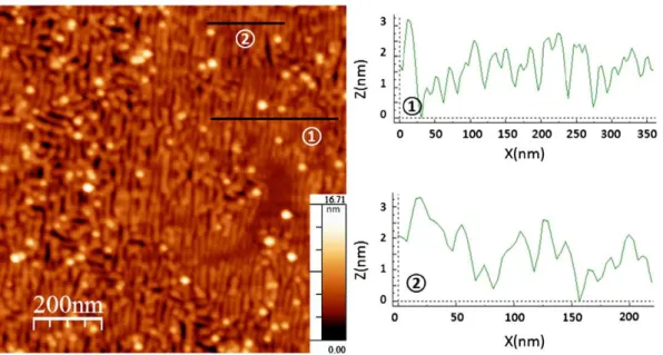
The topography of domains was investigated using AFM measure-ments. The same area that was partially covered by domains was ob-served with SEM and AFM (Fig. 10). The black areas in both images correspond to the iridium surfaces that are not covered by domains. After several line scans, an average height of 8.5 ± 0.4 nm was extracted with an RMS of 0.68 nm. This height corresponds to the total height of the domain and furrows, as shown inFig. 15. Among the domains, a mean height of 1.7 ± 0.3 nm was measured for the furrows (Fig. 11). From previously measured thicknesses, a height of 6.8 nm can be deduced for the thin film deposited on the roughened iridium surface. This value is confirmed by a comparison with the equivalent thickness deduced by XPS, which is discussed in further detail in the next section.
3.7. Nano-Auger analysis of the surface chemistry of domains 3.7.1. After the BEN step
The surface chemistry of the domains was evaluated on a nanometric scale. Nano-Auger was used to compare the dense areas of the domains with the surrounding iridium surface.
Single crystalline diamond (line) and HOPG graphite (···) were used as references. The C KVV Auger spectrum for domains (···) Fig. 6. SEM image of the iridium surface after BEN with the furrows highlighted. The
brightness and contrast adjustments signify the presence of furrows in the domains.
appears very similar to the diamond reference (Fig. 12b). Fine Auger structures in the two pointed areas ofFig. 12a are demonstrated by considering d2N(E)/dE2
. In this case, inflexion points, namely, A1,
A2, A3 and A0, can be accurately determined (Fig. 13a), and their
energy positions are compared with the principal inflexion point A0.
These points correspond to KVV, A0− ŋw and π → π ∗ transitions as described in the literature[14]. The energy differences versus the A0point are reported inFig. 13b for each inflexion point. This
histo-gram demonstrates that the energy values are equivalent inside as well as outside the domains. In addition, these values do not corre-spond exactly to the value determined on the diamond (C*) or HOPG references but correspond instead to the values reported by Constant et al.[14], which were obtained on an amorphous carbon reference.
3.7.2. After a short growth step
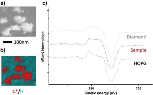
Fig. 14a shows the secondary electron image (SEI) of a sample after a short growth step of 5 min. Nano-Auger cartography was performed in this area to differentiate diamond and iridium. The bi-color image inFig. 14b is the combination of the iridium and dia-mond scans. The red areas that correspond to the bright areas of the SEI image contain the same Auger signature as the diamond reference (C*). This observation is supported by the spectra shown inFig. 14c. 4. Discussion
Several studies have focused on the BEN step on iridium to facili-tate the understanding of heteroepitaxial diamond growth [1,9].
However, some uncertainty remains regarding the unique nucleation pathway. In this study, modifications of the evolution of surface mor-phology and surface chemistry induced by BEN are combined on a nanometric scale.
Our SEM study supports the presence of diamond nuclei after the BEN step. At a low acceleration voltage (0.5 kV), the secondary emission (SE) signal of the extreme surface is greater than the SE signal at 20 kV, and contrast heterogeneities can be detected within the domains (Fig. 4c). After growth, diamond nanocrystals, which are limited to the contrast heterogeneities previously observed after BEN (Fig. 4d), were identified by nano-Auger (Fig. 14). Con-trast heterogeneities within the domains can be correlated to the presence of several carbon phases with different SE yields at the surface. According to the literature, a factor of 300 was reported be-tween the SE yield of diamond and the one of amorphous carbon at 0.5 kV[15].
The colocalization between the heterogeneities observed after BEN in the domains and diamond nanocrystals after a short growth strongly suggests the presence of diamond nuclei prior to the growth step. These nuclei are most likely located at the interface with iridium. Their presence is a required condition to obtain a registry of heteroepitaxial diamond with iridium lattice (Fig. 3). This assumption can be further corroborated by the nano-Auger results. This hypothesis is consistent with a previous study by Schreck et al. After a maximum annealing of 1000 °C, dark regions were observed by the in-lens detector instead of the bright domains that were observed after the BEN step[16]. This reduction in contrast may indicate the thermal transformation of diamond nuclei into carbon onions. Such a temperature causes a surface graphitization of diamond detonation nanoparticles of 5 nm [17]. Graphite plays an important role in the electron emitting process by limiting the field emission properties of diamond nanocrystals[18]. This finding may explain the faded contrast.
In this study, domains exhibit a particular topography after the BEN step compared with the topography in other studies. In our case, the domains are composed of a thin film of amorphous carbon deposited on furrows with diamond nuclei at the interface, as repre-sented byFig. 15.
In part 3.6, the height of the dense domains and the height of the furrows were measured successively as 8.5 ± 0.4 nm and 1.7 ± 0.3 nm, respectively, in the same area by AFM analysis. After subtraction, a thin film of approximately 6.8 nm is deposited on the furrows. This value deduced by calculation was confirmed by XPS analysis. The ratio of C 1s and Ir 4d5/2XPS peaks leads to the
determi-nation of an equivalent carbon thickness deq, assuming a
homoge-neous carbon overlayer[10,11]. This estimated equivalent thickness of carbon from XPS corresponds to 6.7 nm deposited on the iridium surface.
In the literature, the height of the furrows reported by Schreck et al. is approximately 3 nm[8]. Our height of 1.7 ± 0.3 nm is of Fig. 8. SEM images of the domain evolution according to the duration of the BEN step: (a) isolated domains after 30 min and (b) domain coalescence after 60 min.
Fig. 10. Correlation between (a) SEM image a (b) AFM image of the same areas exhibiting domains after BEN; (c) line scans from AFM image.
the same order of magnitude. Schreck et al. reported the domain to-pography corresponding to a 1 nm deep depression compared with the surface of the surrounding area[19]. Our investigations indicate that the domains are composed of an overlayer that is 8.5 ± 0.4 nm thick. This difference in domain topography is most likely due to dif-ferent BEN conditions employed by both groups.
To complete the topography description of the domain, a nano-AES analysis was performed on the dense domains. The analysis did not re-veal any chemical composition equivalent to diamond or HOPGraphite. However, the Auger signature of the domains resembles an amorphous carbon layer[14](Fig. 13).
For the heterogeneities observed by SEM analysis after the BEN step, we cannot detect any difference in the nature of the carbon phases using nano-Auger. The depth probed by this technique is low compared to the carbon thickness measured by XPS analysis. Depths in the range of 1–2 nm are estimated compared to a depth of 6.7 nm. This result supports the presence of diamond nuclei at the interface between the iridium roughening and the deposition of a thin film of amorphous carbon, as previously described. The obser-vation of heteroepitaxial diamond crystals on iridium after a short growth step strongly supports this hypothesis (Fig. 3).
The last point to be discussed is the relation between furrow and domain formation. Most studies on diamond heteroepitaxy from the
iridium surface report this specific substrate roughening after the BEN step [5,7,9,13]. In this study, SEM analyses demonstrate that the presence of roughening is closely related to furrows. This type of roughening appears only during the BEN step. According to SEM observations, morphologies of furrows are not modified after the growth step.
After 30 min of the BEN step, parallel patterns are observed along [010] and [100] directions of the iridium surface (Fig. 7a). This mor-phological surface evolution of iridium can be attributed to the ion beam bombardment during the BEN step. Similar patterns of metallic surfaces after focused ion beam (FIB) exposure have been reported in the literature. This exposure, which is named the ‘ion sandblasting’ phenomenon [20], is analogous with the action of wind on sand dunes. If there is a defect at the surface, these patterns change their direction of propagation along the steps of terraces, as shown in
Fig. 7and described in the literature. The form, lateral periodicity and orientation of ripples are dependent on the flux, energy, and inci-dence angle of the ions, as well as the surface temperature.
Bauer[5]demonstrated that when the methane ratio injected in plasma is modified, these ripples can be created preferentially at the surface. The bias voltage can also control these patterns[13].
Domains without furrows were never observed during multiple SEM observations. This absence may indicate a strong correlation Fig. 12. a) Localizations of nano-Auger analysis outside the domains and inside the domains and b) comparison of C KVV Auger spectra for the HOPG sp2reference (···), the
Diamond sp3(C*) reference (line), and outside (−−) and inside (···) the domains after BEN using the derivative mode (dN(E)/dE normalized to [0,1]).
Fig. 13. a) Comparison of C KVV Auger spectra for the HOPG sp2reference (···), diamond sp3(C*) reference (line) and outside (−−) and inside (···) the domains after BEN using the
de-rivative mode (d2N(E)/dE2normalized to [0,1]) and b) difference in energy of each inflexion point versus A
0point measured on d2N(E)/dE2of AES spectra acquired in the domains, outside the
between furrow and domain formation. The presence of furrows is required but not sufficient for the appearance of domains. In the literature, furrows are always observed in SEM images with do-mains, whether parallel or not parallel with other forms (cubic morphology and dots). By tuning the bias voltage[13], the optimum surface coverage of diamond after the growth step corresponds to the surfaces of domains with furrows equivalent to dots. Subse-quently, the TEM analysis of cross sections indicates that there is no interface layer between the iridium and the diamond after the growth step[7]. The XPD analysis demonstrated that there is a dia-mond signature after the BEN step inside the domains[21]. This finding was obtained by Hoffman et al. using HR-EELS analysis. In the latter case, the detected nuclei are covered by a thin and weakly bonded amorphous or highly defective hydrogenated carbon layer after the BEN step[22].
This study has highlighted that the formation of domains requires furrows. We believe that they can act as channels to facilitate carbon super-saturation to induce the nucleation sites of diamond. The local-ization of these diamond nuclei are observed at significantly low accel-eration voltages by SEM analysis prior to the growth step. A similar hypothesis was proposed by Kawarada et al. on β-SiC substrate[23]. The presence of β-SiC protrusions that resemble furrows, which are named grooves, was assumed to initiate the growth of heteroepitaxial diamond from the Volmer–Weber mode.
5. Conclusions
The topography and surface chemistry of iridium surfaces were simultaneously monitored after each step of the nucleation process and growth step. Observations of localized areas were performed on a nanoscale using SEM, AFM and nano-Auger. This multi-technique approach provides new experimental data that improve the knowl-edge of nucleation pathways on iridium.
SEM imaging at a low acceleration voltage enables the detection of diamond nuclei or stable precursors after BEN. After a short growth step, diamond nanocrystals were probed at similar locations by SEM and nano-Auger. Domains were composed of an amorphous carbon overlayer with a thickness of 6.8 nm, as confirmed by AFM and XPS data. Diamond nuclei probed after the BEN step are most likely located at the interface with iridium. It is a required condition to get highly oriented diamond after growth (Fig. 3). This assumption is confirmed by the nano-Auger experiment performed after the BEN step. The analyzed depths (1–2 nm) are insufficient to probe dia-mond nuclei. Consequently, the Auger C KVV signal obtained is similar to the amorphous carbon reference that corresponds to the carbon overlayer.
Our SEM observations also suggest a close relationship between the furrows created under ion bombardment and the domains created under our conditions. No domain was found without the presence of
Fig. 15. Drawing of domain (carbon thin film + furrows) at the iridium surface with thicknesses extracted from AFM, diamond nuclei which are represented at the interface with iridium according to SEM and nano-Auger.
Fig. 14. Nano-Auger analysis after 5 min of growth with (a) SEI image, (b) chemical mapping of C*/Ir with C* AES diamond signal and (c) spectra of diamond (line), HOPGraphite (∙∙∙∙∙) references and sample (−−−).
furrows. In the furrows, carbon super-saturation, which is required to form diamond nuclei may be easily achieved. According to these results, a sketch was proposed that describes the topography and surface chemistry of the domains (Fig. 15).
Acknowledgments
The authors would like to thank B. Vilquin for the XRD measure-ments and J. Faerber and H. A. Girard for their helpful discussions. References
[1] M. Schreck, T. Bauer, S. Gsell, F. Hörmann, H. Bielefeldt, B. Stritzker, Diam. Relat. Mater. 12 (2003) 262–267.
[2] T. Fujisaki, M. Tachiki, N. Taniyama, M. Kudo, H. Kawarada, Diam. Relat. Mater. 12 (2003) 246–250.
[3] M. Schreck, H. Roll, B. Stritzker, Appl. Phys. Lett. 74 (1999) 650.
[4] T. Saito, S. Tsuruga, N. Ohya, K. Kusakabe, S. Morooka, H. Maeda, et al., Diam. Relat. Mater. 7 (1998) 1381–1384.
[5] T. Bauer, S. Gsell, F. Hörmann, M. Schreck, B. Stritzker, Diam. Relat. Mater. 13 (2004) 335–341.
[6] F. Hörmann, Diam. Relat. Mater. 9 (2000) 256–261.
[7] A. Sawabe, H. Fukuda, T. Suzuki, Y. Ikuhara, T. Suzuki, Surf. Sci. 467 (2000) L845–L849.
[8] F. Hörmann, M. Schreck, B. Stritzker, Diam. Relat. Mater. 10 (2001) 1617–1621. [9] B. Golding, C. Bednarski-Meinke, Z. Dai, Diam. Relat. Mater. 13 (2004) 545–551. [10] A. Chavanne, J.-C. Arnault, J. Barjon, J. Arabski, Surf. Sci. 605 (2011) 564–569. [11] A. Chavanne, J. Barjon, B. Vilquin, J. Arabski, J.C. Arnault, Diam. Relat. Mater. 22
(2012) 52–58.
[12] A. Chavanne, PhD, Université de Versailles Saint -Quentin-en-Yvelines, 2011. [13] M. Regmi, K. More, G. Eres, Diam. Relat. Mater. 23 (2012) 28–33.
[14] L. Constant, C. Speisser, F. Le Normand, Surf. Sci. 387 (1997) 16. [15] D. Joy, A Database on Electronic–Solid Interactions, 2001.
[16] S. Gsell, M. Schreck, T. Bauer, H. Karl, G. Thorwarth, A. Bergmaier, et al., Diam. Relat. Mater. 14 (2005) 328–334.
[17] T. Petit, J.-C. Arnault, H.A. Girard, M. Sennour, P. Bergonzo, Phys. Rev. B 84 (2011) 3407.
[18] K. Wu, E.G. Wang, Z.X. Cao, J. Appl. Phys. 88 (2000) 2967–2974.
[19] S. Gsell, M. Schreck, G. Benstetter, E. Lodermeier, B. Stritzker, Diam. Relat. Mater. 16 (2007) 665–670.
[20] U. Valbusa, C. Boragno, F.B. de Mongeot, J. Phys. Condens. Matter 14 (2002) 8153–8175.
[21] S. Gsell, S. Berner, T. Brugger, M. Schreck, R. Brescia, M. Fischer, et al., Diam. Relat. Mater. 17 (2008) 1029–1034.
[22] A. Hoffman, S. Michaelson, R. Akhvlediani, N.K. Hangaly, S. Gsell, R. Brescia, et al., Phys. Status Solidi A 206 (2009) 1972–1977.

![Fig. 13. a) Comparison of C KVV Auger spectra for the HOPG sp 2 reference (···), diamond sp 3 (C*) reference (line) and outside (−−) and inside (···) the domains after BEN using the de- de-rivative mode (d 2 N(E)/dE 2 normalized to [0,1]) and b) differe](https://thumb-eu.123doks.com/thumbv2/123doknet/13254175.396263/9.892.199.708.76.319/comparison-spectra-reference-diamond-reference-outside-rivative-normalized.webp)